Semiconductor Workforce Automation Market Insights
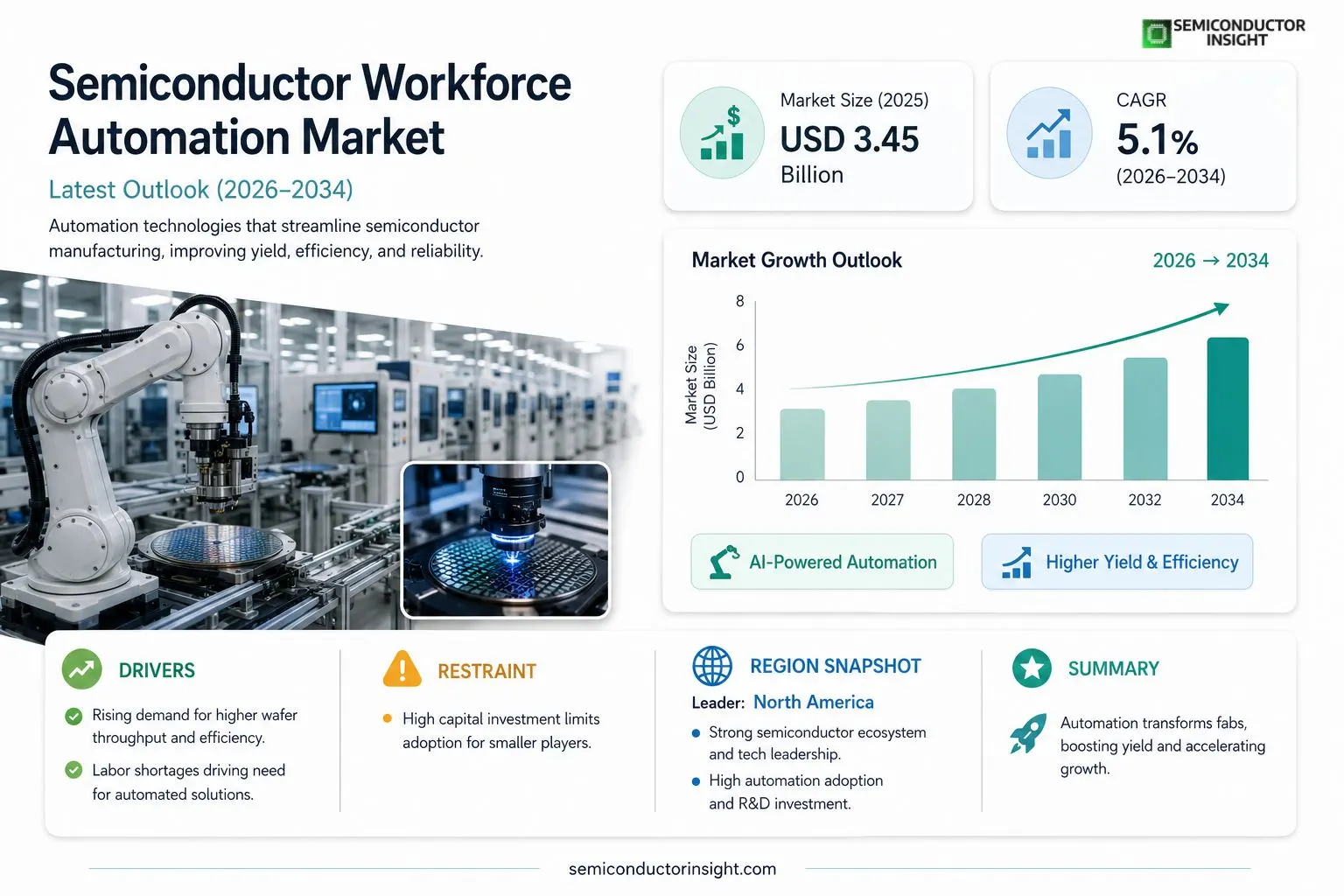
Global semiconductor workforce automation market size was valued at USD 3.45 billion in 2025. The market is projected to grow from USD 3.78 billion in 2026 to USD 5.62 billion by 2034, exhibiting a CAGR of 5.1% during the forecast period.
Workforce automation in semiconductor manufacturing encompasses robotic material handling, AI‑driven defect inspection, and autonomous wafer‑processing systems that streamline production lines and reduce human error. These technologies integrate machine vision, predictive analytics, and real‑time process control to enhance yield and throughput while maintaining strict clean‑room standards.The market is experiencing rapid growth due to rising capital expenditure on advanced node fabs, increasing demand for high‑performance computing chips, and the pressure to shorten time‑to‑market. Furthermore, labor shortages in high‑skill regions are driving fabs toward automated solutions. Key players such as ASML Holding, KLA Corporation, and Tokyo Electron are expanding their automation portfolios through strategic partnerships and R&D investments, further accelerating market expansion.
MARKET DRIVERS
Increasing Production Efficiency
Semiconductor Workforce Automation Market is being propelled by manufacturers’ need to boost wafer throughput while reducing cycle times. Automation platforms now achieve up to 30% higher yield by synchronizing robotics with real‑time defect analytics, allowing fabs to meet the demand for advanced nodes without proportional labor expansion.
Advanced AI Integration
Embedding AI-driven decision engines into automation suites enables predictive maintenance and dynamic scheduling. Companies report a 15% reduction in unplanned equipment downtime, directly translating to higher capacity utilization and lower operational costs across Semiconductor Workforce Automation Market.
➤ “AI‑enabled bots are now the backbone of 7‑nm and 5‑nm production lines, delivering consistency that manual processes cannot match.”
These efficiency gains are further amplified by the growing adoption of digital twins, which provide a virtual replica of the fab floor. By simulating process flows, manufacturers can optimize labor allocation before physical deployment, reinforcing the growth trajectory of Semiconductor Workforce Automation Market.
MARKET CHALLENGES
Skill Gap and Training
Despite rapid technology adoption, the industry faces a shortage of workers proficient in robotics programming and data analytics. Surveys indicate that 45% of fabs cite insufficient in‑house expertise as a barrier to full automation deployment, forcing reliance on external consultants and extending project timelines.
Other Challenges
Regulatory Compliance
Stringent environmental and safety standards require automated systems to meet specific emissions and waste‑handling protocols. Compliance audits can add up to 12 months to implementation schedules, delaying ROI realization for many investors in Semiconductor Workforce Automation Market.
MARKET RESTRAINTS
High Capital Expenditure
Deploying fully integrated automation lines demands upfront capital outlays that can exceed $200 million for a mid‑size fab. Smaller players often lack the financial bandwidth to undertake such investments, creating a market segmentation that favors large incumbents.
Legacy Infrastructure Compatibility
Older equipment architectures frequently lack open interfaces, necessitating costly retrofits or complete replacements. This technical incompatibility restrains adoption rates, especially in regions where older fabs dominate the production landscape.Consequently, the overall pacing of Semiconductor Workforce Automation Market is moderated by these financial and technical constraints, prompting vendors to offer modular solutions that lower entry barriers.
MARKET OPPORTUNITIES
Emergence of Edge Computing
Edge‑enabled controllers allow real‑time processing of sensor data directly on the shop floor, reducing latency and enhancing decision speed. This capability opens new opportunities for decentralized automation models, particularly in high‑mix, low‑volume production environments.
Customizable Automation Solutions
Software‑defined automation platforms now support plug‑and‑play modules tailored to specific process steps such as lithography alignment or wafer inspection. The flexibility to reconfigure workflows without extensive hardware changes positions vendors to capture a broader share of the evolving Semiconductor Workforce Automation Market.Additionally, the rise of collaborative robots (cobots) that work safely alongside humans is creating hybrid work environments. These cobots can handle repetitive tasks while skilled engineers focus on process optimization, further expanding the addressable market and delivering tangible productivity gains.
Semiconductor Workforce Automation Market Trends
Integration of AI‑Driven Inspection Systems
Semiconductor Workforce Automation Market is seeing a decisive shift toward AI‑driven defect inspection across advanced fabs. Machine‑vision sensors combined with deep‑learning algorithms now identify sub‑micron anomalies in real time, reducing reliance on manual visual checks. This transition improves yield by catching pattern deviations earlier in the process flow and aligns with clean‑room protocols that limit human contact. Operators benefit from predictive alerts that suggest corrective actions before a defect propagates, thereby shortening cycle times and enhancing overall equipment effectiveness.
Other Trends
Robotic Material Handling Expansion
Robotic material handling represents a second major pillar of Semiconductor Workforce Automation Market. Autonomous guided vehicles (AGVs) and collaborative robots now transport wafers, carriers, and chemicals between process modules with millimeter precision. By integrating real‑time location systems and predictive maintenance analytics, these robots minimize downtime caused by material bottlenecks. The broader adoption is driven by continued capital investment in high‑density fabs where human ergonomics and labor shortages present operational risks. As a result, fabs are redesigning floor layouts to accommodate parallel robotic pathways, which further strengthens throughput and reduces the probability of contamination.
Strategic Partnerships and Portfolio Diversification
Leading equipment suppliers are forging strategic partnerships to broaden their automation portfolios, a trend that accelerates Semiconductor Workforce Automation Market. Collaborative R&D programs with AI specialists enable the rollout of integrated control platforms that unify wafer‑processing, metrology, and inspection tools under a single supervisory interface. These platforms deliver seamless data exchange, allowing production planners to synchronize scheduling decisions with real‑time quality metrics. Consequently, fabs achieve higher operational agility, responding faster to market demand for high‑performance computing chips while maintaining stringent yield targets.
COMPETITIVE LANDSCAPEKey Industry Players
Semiconductor Workforce Automation Market Overview
Semiconductor Workforce Automation Market, valued at USD 3.45 billion in 2025, is dominated by a few vertically integrated equipment manufacturers that combine lithography, inspection and process control into a single automation suite. ASML Holding leads the landscape by leveraging its high‑NA lithography platforms to embed robotic wafer‑handling and AI‑driven defect inspection. KLA Corporation follows with a deep portfolio of process‑control and yield‑optimization tools that now include autonomous inspection cells. Tokyo Electron (TEL) expands its wafer‑fab automation through strategic partnerships that integrate predictive analytics with real‑time equipment orchestration, positioning the trio as the primary drivers of market growth and standard‑setting.Beyond the top three, a broader set of niche innovators enriches the competitive environment. Applied Materials and Lam Research supply specialized material‑handling robots and plasma‑process automation that target advanced‑node fabs. Advantest and Teradyne focus on AI‑enabled test and inspection stations, while Nikon and Hitachi High‑Tech provide precision machine‑vision solutions for clean‑room environments. Samsung Electronics, though primarily a fab customer, offers proprietary wafer‑level automation modules that compete on cost and integration speed. Smaller specialists such as Artemis Intelligent Systems, SmartRobotics Inc., and e‑Solutions Ltd. deliver modular robotic pick‑and‑place cells and custom software stacks, creating a vibrant ecosystem of best‑of‑breed components.
List of Key Semiconductor Workforce Automation Companies Profiled
- ASML Holding
- KLA Corporation
- Tokyo Electron
- Applied Materials
- Lam Research
- Advantest
- Teradyne
- Nikon
- Hitachi High‑Tech
- Samsung Electronics
- Artemis Intelligent Systems
- SmartRobotics Inc.
- e‑Solutions Ltd.
Segment Analysis:
| Segment Category | Sub-Segments | Key Insights |
| By Type |
|
Robotic Material Handling
|
| By Application |
|
Lithography Automation
|
| By End User |
|
Foundries
|
| By Technology |
|
Machine Vision Systems
|
| By Process Stage |
|
Wafer Fabrication
|
Regional Analysis: North America
United States
The integration of robotic process automation (RPA) and advanced equipment control systems is a key driver in this sector. Manufacturers are deploying robots for tasks such as assembly, testing, and material handling, significantly improving speed and accuracy.
Sophisticated software platforms are being implemented to analyze production data, predict equipment failures, and optimize workflows. These analytics tools enable proactive maintenance and informed decision-making.
Artificial intelligence is increasingly utilized for quality control, process optimization, and predictive maintenance. AI algorithms can detect anomalies and identify potential issues before they escalate, minimizing downtime and maximizing efficiency.
Advanced vision systems are used for automated inspection, defect detection, and precise alignment of components. These systems enhance product quality and reduce the need for manual visual checks.
Europe
The European Semiconductor Workforce Automation Market is witnessing steady growth, driven by government support for the semiconductor industry and a growing focus on sustainable manufacturing practices. While not as dominant as the U.S., Europe boasts a strong base of established semiconductor manufacturers and a skilled workforce. Investment in automation is primarily focused on improving energy efficiency and reducing waste within existing production facilities. The region is also exploring collaborative automation solutions to address labor challenges. The emphasis on data privacy regulations is influencing the development of AI solutions in this market.
Asia-Pacific
Asia-Pacific, particularly China, is emerging as a significant player in Semiconductor Workforce Automation Market. Massive investments in expanding domestic semiconductor manufacturing capabilities are driving demand for automation solutions. The focus is on achieving high-volume production with increased efficiency and reduced costs. Government policies promoting technological self-reliance are further fueling this growth. The market is characterized by a competitive landscape with both domestic and international vendors vying for market share. A key trend is the adoption of automation to support the rapidly evolving demands of the consumer electronics sector within the region.
South America
Semiconductor Workforce Automation Market in South America is currently in its nascent stages. While the region has a growing electronics manufacturing sector, investment in automation remains relatively limited. However, increasing demand for semiconductors in automotive and telecommunications industries is expected to drive future growth. The adoption of automation will be influenced by the availability of skilled labor and the cost of implementation. Government initiatives aimed at fostering technological development could play a crucial role in stimulating market growth in the coming years.
Middle East & Africa
The Middle East & Africa region represents a smaller, but potentially high-growth market for Semiconductor Workforce Automation. Significant investments in infrastructure development and diversification of economies are creating opportunities for expansion in the electronics manufacturing sector. The adoption of automation is driven by the need to improve efficiency and reduce reliance on manual labor. The region’s focus on smart city initiatives and industrial digitalization is expected to further accelerate the growth of the market. However, challenges such as limited skilled workforce and high initial investment costs may hinder rapid adoption.
Report Scope
This market research report provides a comprehensive analysis of the Semiconductor Workforce Automation Market , covering the forecast period 2026–2034. It offers detailed insights into market dynamics, technological advancements, competitive landscape, and key trends shaping the industry.
Key focus areas of the report include:
- Market Overview: The report begins with an overview outlining its current market scenario, key growth indicators, and industry transformation drivers. It discusses macroeconomic factors, demand–supply balance, regulatory landscape, and the strategic role of semiconductors in powering advancements across industries such as automotive, telecommunications, consumer electronics, and industrial automation.
- Market Size & Forecast: Historical data and future projections for revenue, unit shipments, and market value across major regions and segments.
- Segmentation Analysis: Detailed breakdown by product type, technology, application, and end-user industry to identify high-growth segments and investment opportunities.
- Regional Insights: Insights into market performance across North America, Europe, Asia-Pacific, Latin America, and the Middle East & Africa, including country-level analysis where relevant.
- Competitive Landscape: Profiles of leading market participants, including their product offerings, R&D focus, manufacturing capacity, pricing strategies, and recent developments such as mergers, acquisitions, and partnerships.
- Technology Trends & Innovation: Assessment of emerging technologies, integration of AI/IoT, semiconductor design trends, fabrication techniques, and evolving industry standards.
- Market Drivers & Restraints: Evaluation of factors driving market growth along with challenges, supply chain constraints, regulatory issues, and market-entry barriers.
- Stakeholder Insights: Insights for component suppliers, OEMs, system integrators, investors, and policymakers regarding the evolving ecosystem and strategic opportunities.
Primary and secondary research methods are employed, including interviews with industry experts, data from verified sources, and real-time market intelligence to ensure the accuracy and reliability of the insights presented.
FREQUENTLY ASKED QUESTIONS:
What is the current market size of Semiconductor Workforce Automation Market?
-> Semiconductor Workforce Automation Market was valued at USD 3.45 billion in 2025 and is expected to reach USD 5.62 billion by 2034.
Which key companies operate in Semiconductor Workforce Automation Market?
-> Key players include ASML Holding, KLA Corporation, and Tokyo Electron, among others.
What are the key growth drivers?
-> Key growth drivers include rising capital expenditure on advanced node fabs, increasing demand for high‑performance computing chips, pressure to shorten time‑to‑market, and labor shortages in high‑skill regions.
Which region dominates the market?
-> The reference emphasizes a global market; major activity is concentrated in regions with advanced semiconductor fabs, notably Asia‑Pacific, North America, and Europe.
What are the emerging trends?
-> Emerging trends include AI‑driven defect inspection, autonomous wafer‑processing systems, and robotic material handling integrated with machine vision and predictive analytics.

Get Sample Report PDF for Exclusive Insights
Report Sample Includes
- Table of Contents
- List of Tables & Figures
- Charts, Research Methodology, and more...
 Download Sample Report PDF