
Semiconductor Wafer Bonding Equipment Market Insights
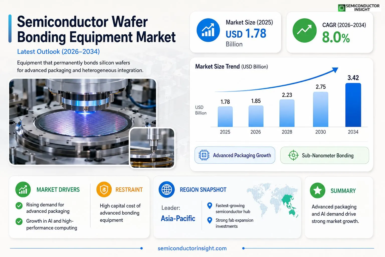
Global Semiconductor Wafer Bonding Equipment Market size was valued at USD 1.78 billion in 2025. The market is projected to grow from USD 1.85 billion in 2026 to USD 3.42 billion by 2034, exhibiting a CAGR of 8.0% during the forecast period.
Semiconductor wafer bonding equipment enables the permanent joining of two or more silicon wafers through processes such as direct silicon‑to‑silicon bonding, anodic bonding, plasma‑activated bonding and thermocompression bonding. These systems provide precise temperature control, surface activation and alignment capabilities that are essential for advanced packaging technologies like heterogeneous integration and fan‑out wafer‑level packaging.The market is experiencing rapid growth because demand for high‑performance computing, AI accelerators and miniaturized sensors drives adoption of advanced packaging solutions that rely on reliable wafer bonds. Furthermore, rising investments in fab expansions across Asia‑Pacific and North America accelerate equipment purchases. Key players such as EV Group, SUSS MicroTec, Tokyo Electron and CVD Equipment are expanding their portfolios; for example, EV Group launched a next‑generation high‑throughput bonding platform in early 2024 that promises sub‑nanometer gap control.
MARKET DRIVERS
Rising Demand for Advanced Packaging
Semiconductor Wafer Bonding Equipment Market is being propelled by the exponential growth of advanced packaging solutions such as 3D‑ICs and system‑in‑package (SiP). Manufacturers are adopting these technologies to achieve higher performance and miniaturization, driving a projected 12% CAGR through 2032. The shift from traditional wire‑bonding to wafer‑level bonding is creating a robust pipeline of capital expenditures.
Technological Innovation in Bonding Techniques
Recent breakthroughs in low‑temperature direct bonding and plasma‑activated surface treatment have reduced defect rates by up to 30%, enhancing yield for high‑value chips. These innovations are encouraging OEMs to upgrade legacy lines, thereby expanding the addressable market for new equipment models.
➤ Industry surveys indicate that over 65% of leading fabs plan to increase wafer bonding capacity within the next three years.
In addition, the proliferation of 5G infrastructure and automotive electronics is intensifying the need for high‑density interconnects, reinforcing the long‑term growth trajectory of Semiconductor Wafer Bonding Equipment Market.
MARKET CHALLENGES
High Capital Intensity
Deploying state‑of‑the‑art bonding platforms requires multiyear investments, often exceeding $150 million per fab. This financial barrier can delay adoption, especially among midsize manufacturers who lack sufficient liquidity.
Other Challenges
Process Integration Complexity
Integrating wafer bonding with existing lithography and etch flows demands precise thermal and mechanical alignment. Misalignment can lead to yield losses, making the transition to newer equipment risky without extensive pilot testing.
MARKET RESTRAINTS
Limited Skilled Workforce
The specialized nature of wafer bonding processes requires engineers with niche expertise in surface chemistry and precision mechanics. Global talent shortages are constraining the speed at which fabs can fully staff new lines, thereby tempering market expansion.Moreover, stringent cleanroom standards increase operational overhead, and any deviation can result in costly rework, further discouraging rapid scale‑up of bonding capacity.
MARKET OPPORTUNITIES
Emerging Applications in Quantum Computing
Quantum hardware demands ultra‑low defect bonding for photonic and superconducting chips. Vendors that can deliver sub‑nanometer alignment and cryogenic‑compatible equipment are positioned to capture a high‑margin niche within the broader market.
Growth of Flexible and Heterogeneous Integration
Flexible electronics and heterogeneous integration platforms are expanding the addressable substrate pool beyond traditional silicon. Equipment manufacturers offering adaptable tooling for glass, polymer, and compound semiconductor wafers will benefit from diversified revenue streams.Finally, strategic collaborations between equipment producers and material suppliers are accelerating the rollout of next‑generation bonding adhesives and intermediates, unlocking new performance thresholds and creating fresh demand cycles.
Semiconductor Wafer Bonding Equipment Market Trends
Growth Fueled by Advanced Packaging Demand
Semiconductor Wafer Bonding Equipment Market is experiencing a rapid acceleration as manufacturers of high‑performance computing systems, artificial‑intelligence accelerators, and compact sensors seek reliable wafer‑level interconnects. Advanced packaging technologies such as heterogeneous integration and fan‑out wafer‑level packaging depend on precise temperature control, surface activation, and sub‑micron alignment that bonding equipment uniquely provides. Investment cycles in semiconductor fabs across the Asia‑Pacific region and North America have intensified, prompting equipment suppliers to expand production capacity and deliver higher‑throughput platforms. As product roadmaps push toward smaller form factors and greater functionality, demand for bonding solutions that can maintain wafer integrity while reducing cycle time has become a strategic priority for many chipmakers. The market is increasingly regarded as a critical enabler of continued performance scaling.
Other Trends
Technology Innovations
Key technology innovations are reshaping Semiconductor Wafer Bonding Equipment Market. Direct silicon‑to‑silicon bonding, anodic bonding, plasma‑activated bonding, and thermocompression bonding have each seen incremental performance gains. In early 2024 EV Group introduced a next‑generation high‑throughput bonding platform that delivers sub‑nanometer gap control and reduced thermal budget, enabling finer pitch interconnections. SUSS MicroTec and Tokyo Electron have broadened their portfolio with modular systems that integrate real‑time surface‑energy monitoring, while CVD Equipment added AI‑driven recipe optimization to improve yield. These advances not only shorten cycle times but also expand the material palette, supporting emerging applications such as 3‑D heterogeneous integration and advanced sensor stacks. The platforms are designed for compatibility with existing fab footprints, reducing retrofit costs.
Supply Chain and Regional Dynamics
Supply‑chain resilience and regional investment patterns are influencing Semiconductor Wafer Bonding Equipment Market. The concentration of component suppliers in Europe and East Asia creates a logistical balance that many OEMs are addressing through dual‑source strategies. Meanwhile, government‑backed fab expansion programmes in China, South Korea, Taiwan, and the United States have accelerated capital expenditures for wafer bonding tools. This geographic diversification reduces lead times and supports localized production of AI‑centric and automotive semiconductor modules. As the ecosystem matures, collaboration between equipment vendors and chip designers is sharpening, leading to co‑development projects that align bonding system capabilities with next‑generation device architectures. The trend also encourages standardization of interface protocols, allowing easier integration of bonding equipment into automated fab lines.
COMPETITIVE LANDSCAPEKey Industry Players
Semiconductor Wafer Bonding Equipment Market Competitive Overview
The market is anchored by a few dominant suppliers that command the majority of high‑volume orders for advanced packaging lines. EV Group (EVG) leads with its next‑generation high‑throughput bonding platform launched in early 2024, offering sub‑nanometer gap control that is critical for heterogeneous integration. SUSS MicroTec follows closely, leveraging its extensive portfolio of direct wafer bonding and surface activation tools to serve AI accelerator manufacturers. Tokyo Electron (TEL) differentiates through integrated process modules that combine bonding with deposition and etch steps, enabling tighter fab footprints. Applied Materials and ASM International round out the core group, each providing complementary bonding solutions that address both 2.5 D and fan‑out wafer‑level packaging segments, and together they shape the market’s pricing and technology roadmaps.Niche but technically sophisticated players expand the competitive set by focusing on specialized processes. CVD Equipment Corp supplies plasma‑activated bonding tools that excel in low‑temperature applications for sensor integration. Jeol and Nikon offer precision aligner systems prized by research labs and niche fab customers. Coventor and Teledyne deliver modular bonding stations tailored for prototype development and small‑batch production. Additionally, companies such as Advanced Semiconductor Engineering (ASE) and STMicroelectronics provide in‑house bonding capabilities that influence equipment demand patterns, while emerging firms like Nanomaker and Zygo introduce ultrafast laser‑assisted bonding technologies that could reshape future market dynamics.
List of Key Semiconductor Wafer Bonding Equipment Companies Profiled
- EV Group (EVG)
- SUSS MicroTec
- Tokyo Electron (TEL)
- Applied Materials
- ASM International
- CVD Equipment Corp
- Jeol Ltd.
- Nikon Corporation
- Coventor Inc.
- Teledyne Technologies
- Advanced Semiconductor Engineering (ASE)
- STMicroelectronics
- Nanomaker Ltd.
- Zygo Corporation
Segment Analysis:
| Segment Category | Sub-Segments | Key Insights |
| By Type |
|
Direct silicon‑to‑silicon bonding
|
| By Application |
|
Heterogeneous integration
|
| By End User |
|
Semiconductor manufacturers
|
| By Technology Evolution |
|
High‑throughput platforms
|
| By Process Complexity |
|
Advanced multi‑layer bonding
|
Regional Analysis: North America
North America
The United States constitutes the largest share of the North American market, exhibiting consistent growth fueled by substantial government initiatives and private sector investments in semiconductor manufacturing. Strong domestic demand for advanced microprocessors and memory chips underpins the need for sophisticated wafer bonding equipment.
Canada’s semiconductor industry is steadily growing, with increasing investments in research and development and manufacturing capabilities. The demand for wafer bonding equipment is primarily driven by the expansion of the Canadian semiconductor ecosystem and collaborations with international players.
Mexico’s semiconductor sector has emerged as a significant manufacturing hub, attracting investments from global players. The growth of the automotive and industrial sectors is creating demand for advanced semiconductors, thereby driving the need for robust wafer bonding solutions in the region.
Puerto Rico’s semiconductor manufacturing capabilities are focused on specialized segments, generating demand for specific types of wafer bonding equipment. While smaller in scale compared to other North American markets, it plays a crucial role in certain niche applications.
Europe
Europe’s Semiconductor Wafer Bonding Equipment Market is characterized by a strong emphasis on innovation and advanced packaging technologies. Driven by governmental support and a focus on high-tech manufacturing, the region is witnessing a resurgence in semiconductor production. Key trends include investments in advanced lithography, 3D integration, and power electronics, all of which require sophisticated wafer bonding equipment. The interconnected nature of the European semiconductor ecosystem fosters collaboration between research institutions, equipment manufacturers, and semiconductor foundries. The region is also gaining traction in the development of advanced packaging solutions for automotive and industrial applications.
Asia-Pacific
Asia-Pacific continues to be the largest and fastest-growing market for Semiconductor Wafer Bonding Equipment, driven by the dominance of countries like China, Japan, South Korea, and Taiwan. The region’s strong consumer electronics market, combined with heavy investments in artificial intelligence, 5G, and automotive semiconductors, fuels significant demand for advanced wafer bonding solutions. China’s government initiatives to develop a self-sufficient semiconductor industry are a major driver of market growth. The region is also a key center for both equipment manufacturing and semiconductor fabrication.
South America
South America represents a relatively smaller but growing market for Semiconductor Wafer Bonding Equipment. The increasing adoption of electronics in various sectors, including telecommunications, automotive, and consumer goods, is contributing to the demand. Brazil and Argentina are the primary markets in the region, with potential for further growth as industries invest in modernization and technological advancements.
Middle East & Africa
The Middle East & Africa region presents a nascent but promising market for Semiconductor Wafer Bonding Equipment. The expansion of telecommunications infrastructure, increasing adoption of digital technologies, and growing investments in automotive and industrial sectors are driving demand. Countries like Saudi Arabia, the United Arab Emirates, and South Africa are expected to witness significant growth in the coming years as they pursue technological diversification and industrial development.
Report Scope
This market research report provides a comprehensive analysis of the Semiconductor Wafer Bonding Equipment Market , covering the forecast period 2026–2034. It offers detailed insights into market dynamics, technological advancements, competitive landscape, and key trends shaping the industry.
Key focus areas of the report include:
- Market Overview: The report begins with an overview outlining its current market scenario, key growth indicators, and industry transformation drivers. It discusses macroeconomic factors, demand–supply balance, regulatory landscape, and the strategic role of semiconductors in powering advancements across industries such as automotive, telecommunications, consumer electronics, and industrial automation.
- Market Size & Forecast: Historical data and future projections for revenue, unit shipments, and market value across major regions and segments.
- Segmentation Analysis: Detailed breakdown by product type, technology, application, and end-user industry to identify high-growth segments and investment opportunities.
- Regional Insights: Insights into market performance across North America, Europe, Asia-Pacific, Latin America, and the Middle East & Africa, including country-level analysis where relevant.
- Competitive Landscape: Profiles of leading market participants, including their product offerings, R&D focus, manufacturing capacity, pricing strategies, and recent developments such as mergers, acquisitions, and partnerships.
- Technology Trends & Innovation: Assessment of emerging technologies, integration of AI/IoT, semiconductor design trends, fabrication techniques, and evolving industry standards.
- Market Drivers & Restraints: Evaluation of factors driving market growth along with challenges, supply chain constraints, regulatory issues, and market-entry barriers.
- Stakeholder Insights: Insights for component suppliers, OEMs, system integrators, investors, and policymakers regarding the evolving ecosystem and strategic opportunities.
Primary and secondary research methods are employed, including interviews with industry experts, data from verified sources, and real-time market intelligence to ensure the accuracy and reliability of the insights presented.
FREQUENTLY ASKED QUESTIONS:
What is the current market size of Semiconductor Wafer Bonding Equipment Market?
-> Semiconductor Wafer Bonding Equipment Market was valued at USD 1.78 billion in 2025 and is expected to reach USD 3.42 billion by 2034.
Which key companies operate in Semiconductor Wafer Bonding Equipment Market?
-> Key players include EV Group, SUSS MicroTec, Tokyo Electron, CVD Equipment.
What are the key growth drivers?
-> Key growth drivers include high‑performance computing, AI accelerators, miniaturized sensors, demand for advanced packaging solutions, and fab expansion investments in Asia‑Pacific and North America.
Which region dominates the market?
-> Asia‑Pacific is the fastest‑growing region, while North America also shows strong demand.
What are the emerging trends?
-> Emerging trends include heterogeneous integration, fan‑out wafer‑level packaging, high‑throughput bonding platforms with sub‑nanometer gap control.

Get Sample Report PDF for Exclusive Insights
Report Sample Includes
- Table of Contents
- List of Tables & Figures
- Charts, Research Methodology, and more...
 Download Sample Report PDF




