MARKET INSIGHTS
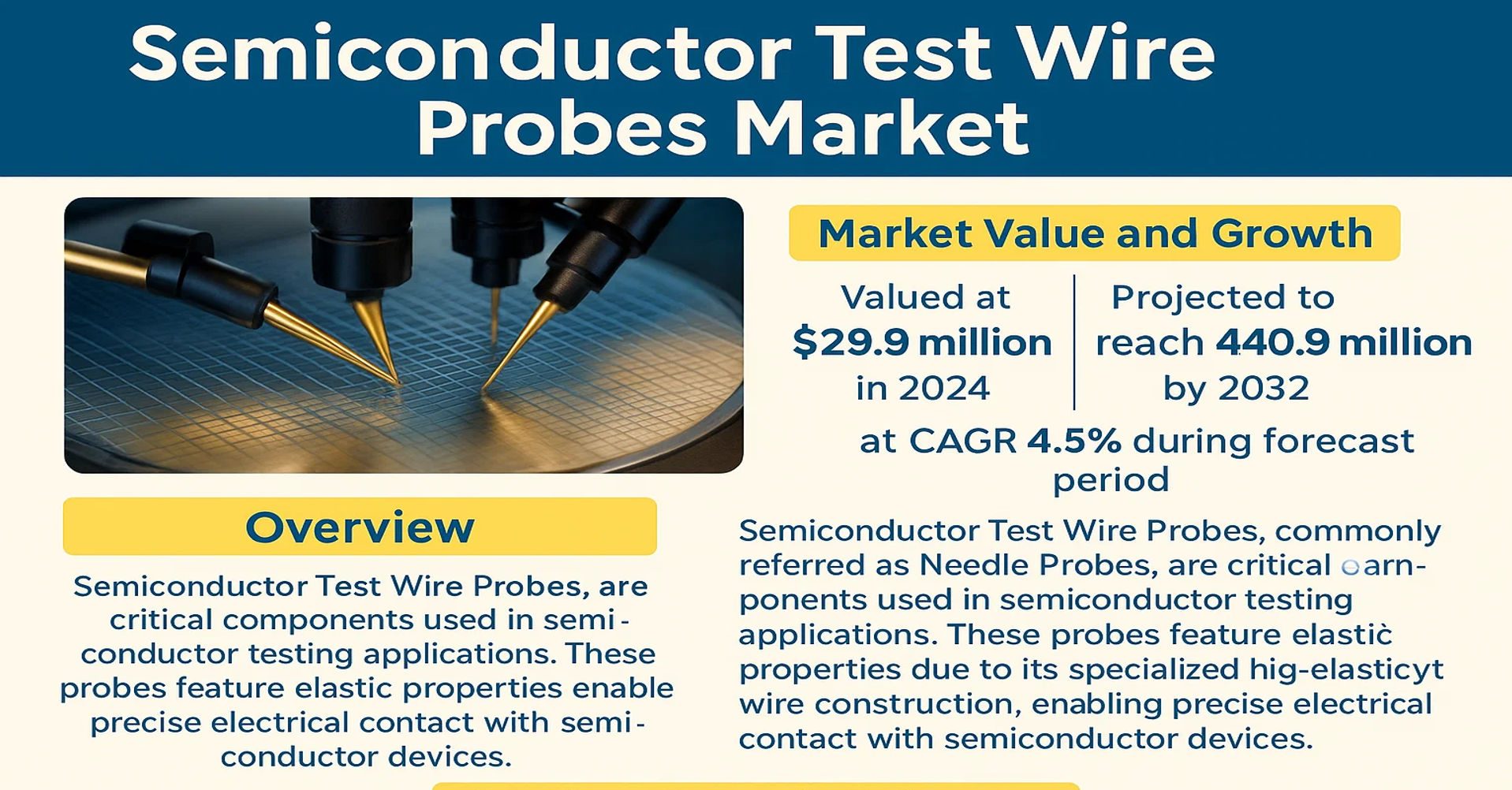
The global Semiconductor Test Wire Probes Market was valued at 29.9 million in 2024 and is projected to reach US$ 40.9 million by 2032, at a CAGR of 4.5% during the forecast period.
Semiconductor Test Wire Probes, commonly referred to as Needle Probes, are critical components used in semiconductor testing applications. These probes feature elastic properties due to their specialized high-elasticity wire construction, enabling precise electrical contact with semiconductor devices. When pressure is applied, the probe generates pin pressure through elastic deformation and restoration forces, making them ideal for testing ICs, wafers, and other microelectronic components.
The market growth is driven by increasing demand for semiconductor manufacturing and testing, particularly in regions like Asia-Pacific where China’s market is expanding rapidly. The Min Pitch: 70 μm segment is expected to show significant growth, catering to advanced semiconductor packaging technologies. Key players such as Tulip Company, Koyo Technos, and TOTOKU INC. dominate the market, with the top five companies holding substantial revenue share in 2024.
MARKET DYNAMICS
MARKET DRIVERS
Rising Semiconductor Industry Demand to Fuel Market Expansion
The global semiconductor industry is experiencing unprecedented growth, with wafer production expected to exceed 30 million units annually by 2030. This surge directly correlates with increased demand for test wire probes, as each semiconductor device requires rigorous testing before reaching the market. The semiconductor test wire probes market is positioned as a critical enabler of this growth, ensuring device reliability and performance consistency across industries. Recent advancements in probe technology have enabled testing of chips with pitches below 50 µm, meeting the stringent requirements of next-generation semiconductor nodes.
Miniaturization of Electronic Components Accelerates Probe Innovation
As electronic devices continue shrinking in size while increasing in complexity, the need for precision test probes has never been greater. The market has responded with innovations in micro-scale probe designs capable of testing components with pitches as small as 70 µm, representing a 40% reduction in size compared to standard probes from just five years ago. This technological leap is particularly crucial for testing advanced packaging solutions like 2.5D and 3D ICs, where traditional probe technologies struggle to maintain signal integrity at such fine pitches.
Quality Assurance Imperatives Drive Market Growth
The semiconductor industry’s zero-defect mandate continues to push testing standards higher, with probe-based testing remaining the most reliable method for wafer-level and final package verification. As automotive and medical applications account for an increasing share of semiconductor consumption, the demand for ultra-reliable probes capable of withstanding millions of test cycles continues to rise. This quality imperative is reflected in the growing market preference for tungsten-based probes, which offer superior durability compared to traditional materials.
MARKET RESTRAINTS
High Development Costs and Complex Manufacturing Processes Limit Market Penetration
The semiconductor test wire probe market faces significant barriers to entry due to the specialized nature of probe manufacturing. Developing probes for sub-70 µm pitches requires precision engineering capabilities that only a handful of manufacturers possess globally. The capital expenditure for establishing a production line capable of manufacturing high-performance probes can exceed several million dollars, creating substantial financial barriers for new market entrants. Additionally, the multi-stage manufacturing process, which includes specialized wire forming, heat treatment, and plating stages, demands highly controlled environments that further increase operational costs.
Supply Chain Vulnerabilities Impact Market Stability
The global semiconductor test probe industry faces mounting challenges from supply chain disruptions, particularly for specialty materials like beryllium-copper and palladium alloys. Recent trade policies and geopolitical tensions have caused significant fluctuations in the availability and pricing of these critical raw materials. Many manufacturers report lead times for certain probe types extending beyond six months, creating bottlenecks in the semiconductor testing ecosystem. These supply chain constraints are particularly problematic for smaller foundries and IDMs that lack long-term supply agreements with probe manufacturers.
Technical Limitations in Ultra-Fine Pitch Testing
While probe technology has advanced significantly, physical limitations emerge as pitches continue shrinking below 50 µm. Issues such as contact resistance variability, probe-to-probe interference, and mechanical reliability become increasingly difficult to manage at these scales. The industry faces particular challenges in maintaining consistent contact force across thousands of probes in array configurations, where even slight variations can impact test results. These technical challenges are driving up R&D costs while slowing the pace of innovation in probe design.
MARKET OPPORTUNITIES
Advanced Packaging Technologies Create New Application Frontiers
The rapid adoption of heterogeneous integration and advanced packaging solutions presents significant growth opportunities for probe manufacturers. Technologies like chiplet architectures require innovative probing solutions capable of testing multiple die configurations at wafer-level. This trend is driving demand for customizable probe arrays that can accommodate varying bump heights and pitches within a single test configuration. Early adopters of these specialized probe solutions are already seeing substantial returns, with some reporting 30% increases in testing efficiency for complex 2.5D packages.
Emerging Semiconductor Applications Drive Probe Innovation
Beyond traditional computing applications, emerging technologies like power semiconductors for electric vehicles and RF components for 5G/6G infrastructure are creating new opportunities in the probe market. These applications demand specialized probe solutions capable of handling higher currents and frequencies than conventional digital IC testing requires. Manufacturers developing probes with enhanced thermal stability and current-carrying capacity are well-positioned to capture these high-growth segments. The market for high-power probe solutions is projected to grow at a CAGR of 7% through 2030, outpacing the overall semiconductor test equipment market.
MARKET CHALLENGES
Maintaining Probe Performance Consistency Across Production Batches
One of the most persistent challenges in semiconductor test wire probe manufacturing is achieving uniformity across production batches. Even minor variations in material composition or heat treatment can significantly impact probe performance, particularly for high-frequency applications. Manufacturers report that maintaining contact resistance within ±5% tolerance across thousands of probes remains an engineering challenge, especially as pitch sizes continue shrinking. These consistency issues become particularly pronounced in high-volume production environments, where even small performance variations can lead to substantial yield losses.
Workforce Specialization Gap Impacts Innovation Pace
The semiconductor test probe industry faces a growing skills gap as experienced probe designers retire and new engineers require extensive training. Developing expertise in probe metallurgy, micro-machining, and high-frequency signal integrity requires years of specialized experience that is increasingly difficult to find. This talent shortage is particularly acute in markets experiencing rapid semiconductor industry expansion, where local workforces lack the specialized skills needed for probe development. Companies are responding by implementing comprehensive training programs, but the lead time to develop proficient engineers remains a constraint on innovation.
Competitive Pressure from Alternative Testing Technologies
While probe-based testing remains the industry standard, emerging technologies like optical and e-beam testing present competitive pressure. These alternative methods offer advantages in certain applications, particularly for ultra-fine pitch devices where physical contact becomes problematic. The market must continue innovating to maintain its position as the preferred testing solution, particularly in sectors like automotive electronics where reliability is paramount. Successful manufacturers are responding by developing hybrid testing solutions that combine traditional probing with complementary technologies.
SEMICONDUCTOR TEST WIRE PROBES MARKET TRENDS
Miniaturization of Semiconductor Devices Driving Demand for High-Precision Probes
The semiconductor industry is witnessing a relentless push toward miniaturization, with advanced packaging technologies like 3D IC and fan-out wafer-level packaging becoming mainstream. This trend directly impacts the semiconductor test wire probes market, where demand for probes with pitches below 70 μm is accelerating. The segment is projected to grow at a notable CAGR through 2032, driven by the need for finer pitch testing in next-generation chips. Probes with elastic deformation properties, known as needle probes, are gaining traction due to their ability to maintain stable contact force even in high-density testing environments. Leading manufacturers are innovating in materials science, adopting specialized high-elasticity alloys that withstand over 1 million test cycles without deformation.
Other Trends
Automation in Testing Processes
Semiconductor test houses are increasingly adopting automated probe card solutions to improve throughput and reduce human error. The integration of AI-driven predictive maintenance systems helps optimize probe lifespan, which typically ranges between 500,000 to 2 million touchdowns depending on application. Automated probe position correction systems are reducing device downtime by 30-40% in high-volume manufacturing environments. This automation wave is particularly pronounced in front-end wafer testing, where test times are being compressed by advanced probe technologies.
Geographic Expansion of Semiconductor Fabs Influencing Probe Demand
The global semiconductor capacity expansion, particularly in Asia and North America, is creating parallel growth opportunities for test probe suppliers. With China’s semiconductor self-sufficiency initiatives driving $142 billion in planned fab investments through 2030, local probe manufacturers are scaling production capabilities. Meanwhile, the U.S. CHIPS Act is catalyzing domestic probe development to support reshored semiconductor manufacturing. Regional demand patterns now show 60-65% of total probe consumption originating from Asia-Pacific fabs, while North American markets are showing the highest growth rate in advanced packaging probe adoption.
Materials Innovation Addressing Wear Challenges
Probe durability remains a critical focus area, with manufacturers developing novel coating solutions featuring tungsten-rhenium alloys and proprietary nanocomposites. These advanced materials demonstrate 40-50% longer service life compared to traditional beryllium copper probes while maintaining stable electrical characteristics. The shift toward rarefied tungsten compositions has proven particularly effective for high-temperature testing applications common in automotive IC validation, where probe temperatures can exceed 150°C during continuous operation.
COMPETITIVE LANDSCAPE
Key Industry Players
Innovation and Precision Drive Market Positioning in Semiconductor Test Wire Probes
The global Semiconductor Test Wire Probes market is characterized by a dynamic and moderately consolidated competitive landscape, with key players focusing on technological advancements to strengthen their market foothold. The market was valued at $29.9 million in 2024 and is projected to expand to $40.9 million by 2032, registering a steady CAGR of 4.5%. Leading companies are investing in R&D to develop specialized needle probes, which cater to the increasing demand for higher precision in semiconductor testing.
Tulip Company and Koyo Technos Co., LTD. dominate the market, collectively accounting for a significant revenue share. These companies capitalize on their expertise in manufacturing high-elasticity wire probes, particularly those with a minimum pitch of ≤70 µm. Their growth is further driven by strategic collaborations with semiconductor foundries and packaging test service providers across Asia and North America.
Meanwhile, mid-sized firms like TOTOKU INC. and TESPRO Co., Ltd. are gaining traction by offering cost-effective solutions for front-end and packaging testing applications. Both companies emphasize durability and repeatability in their probe designs, addressing the critical need for reliability in high-volume semiconductor manufacturing.
The competitive intensity is further heightened by emerging players such as XinFuCheng ShenZhen Electronics, which specializes in customized probe solutions for niche applications. Recent investments in automation and material science have enabled these companies to enhance probe lifespan and signal integrity, key value propositions for advanced semiconductor nodes.
List of Key Semiconductor Test Wire Probes Manufacturers Profiled
- Tulip Company (Japan)
- Koyo Technos Co., LTD. (Japan)
- TOTOKU INC. (Japan)
- TESPRO Co., Ltd. (Japan)
- Elmer Corporation (Japan)
- Nihon Denshin Co. Ltd. (Japan)
- N.C.P.M. Tech Co., Ltd. (South Korea)
- MAUTECKK (Germany)
- XinFuCheng ShenZhen Electronics (China)
Market leaders are also focusing on vertical integration strategies, with several Japanese manufacturers establishing captive probe wire production facilities to ensure quality control and supply chain stability. As the semiconductor industry moves toward more sophisticated testing requirements for 5G and AI chips, these competitive dynamics are expected to intensify further.
Segment Analysis:
By Type
Needle Probes Dominate the Market Due to Their High Elasticity and Precision in Semiconductor Testing
The market is segmented based on type into:
- Needle Probes
- Cantilever Probes
- Vertical Probes
- Others
By Application
Front-end Testing Segment Leads Due to Critical Role in Wafer-Level Testing
The market is segmented based on application into:
- Front-end Testing
- Packaging Testing
- Others
By End User
IDMs Hold Dominant Position Due to Large-scale Semiconductor Manufacturing Operations
The market is segmented based on end user into:
- IDMs (Integrated Device Manufacturers)
- OSATs (Outsourced Semiconductor Assembly and Test Providers)
- Foundries
- Others
By Material
Tungsten-based Probes Maintain Market Leadership for Superior Durability
The market is segmented based on material into:
- Tungsten
- Beryllium Copper
- Phosphor Bronze
- Others
Regional Analysis: Semiconductor Test Wire Probes Market
Asia-Pacific
The Asia-Pacific region dominates the global Semiconductor Test Wire Probes market, driven by rapid semiconductor manufacturing expansion in China, Japan, South Korea, and Taiwan. With semiconductor foundries like TSMC, Samsung, and SMIC aggressively expanding production capacities, demand for high-precision testing solutions is surging. China alone accounts for over 35% of global semiconductor testing equipment demand as domestic wafer fabrication plants prioritize localized supply chains. The region benefits from strong government support, such as China’s “Big Fund” initiative investing $50+ billion in semiconductor self-sufficiency. Japanese manufacturers like TOTOKU and Koyo Technos lead in precision probe technology, while Southeast Asian countries are emerging as cost-effective testing hubs.
North America
Home to leading fabless semiconductor companies and advanced packaging facilities, North America maintains strong demand for high-performance test probes. The U.S. market sees particular growth in front-end testing applications as domestic semiconductor production expands under initiatives like the CHIPS Act. Major probe manufacturers focus on developing ultra-fine pitch (sub-70μm) solutions for 3D IC and advanced packaging testing. However, higher production costs compared to Asian suppliers and reliance on imports for certain probe types present challenges. Collaborative R&D between academia and industry aims to improve probe durability and miniaturization.
Europe
Europe’s market is characterized by specialized demand for automotive and industrial semiconductor testing solutions. German and French manufacturers require probes capable of withstanding harsh environment testing for automotive ICs. The region shows increasing adoption of miniature MEMS probes for IoT and sensor testing applications. European probe suppliers emphasize precision engineering and reliability over mass production, catering to niche markets. However, the lack of large-scale semiconductor fabs in the region limits volume growth compared to Asia. Recent EU semiconductor sovereignty initiatives may boost local testing equipment demand over the long term.
South America
The South American market remains nascent but shows gradual growth in basic semiconductor testing capabilities, primarily supporting consumer electronics assembly. Brazil leads regional demand, though economic fluctuations impact capital investments in testing equipment. Most probes are imported from Asia and North America, with local players focusing on repackaging and redistribution. The lack of advanced semiconductor manufacturing limits demand for high-end test solutions, but increasing electronics production creates opportunities for basic probe suppliers. Political and currency instability continue to hinder market growth potential.
Middle East & Africa
This emerging market shows pockets of development in Israel and UAE, where semiconductor design houses require testing solutions. Israel’s thriving fabless semiconductor ecosystem drives demand for advanced probe technologies, while North African countries primarily import low-cost probes for electronics maintenance. The region lacks domestic probe manufacturing capabilities, relying entirely on imports. Long-term growth potential exists through technology transfer partnerships and increasing electronics manufacturing, but infrastructure limitations slow market development. Recent investments in Egyptian and Saudi tech hubs may gradually increase regional demand.
Report Scope
This market research report provides a comprehensive analysis of the global and regional Semiconductor Test Wire Probes markets, covering the forecast period 2024–2032. It offers detailed insights into market dynamics, technological advancements, competitive landscape, and key trends shaping the industry.
Key focus areas of the report include:
- Market Size & Forecast: Historical data and future projections for revenue, unit shipments, and market value across major regions and segments. The global market was valued at USD 29.9 million in 2024 and is projected to reach USD 40.9 million by 2032, growing at a CAGR of 4.5%.
- Segmentation Analysis: Detailed breakdown by product type (Min Pitch: ≤70 μm, Min Pitch: >70 μm), application (Front-end Testing, Packaging Testing, Others), and end-user industry to identify high-growth segments.
- Regional Outlook: Insights into market performance across North America (U.S., Canada, Mexico), Europe (Germany, France, U.K.), Asia-Pacific (China, Japan, South Korea), and other regions, including country-level analysis.
- Competitive Landscape: Profiles of leading market participants such as Tulip Company, Koyo Technos, TOTOKU INC., TESPRO Co., Ltd., and Elmer Corporation, including their product portfolios, market share, and strategic initiatives.
- Technology Trends & Innovation: Assessment of emerging probe technologies, material advancements, and integration with semiconductor testing equipment.
- Market Drivers & Restraints: Evaluation of factors such as increasing semiconductor production, miniaturization trends, and challenges like high precision requirements and material costs.
- Stakeholder Analysis: Strategic insights for semiconductor manufacturers, test equipment providers, and investors regarding market opportunities and challenges.
The research employs both primary and secondary methodologies, including interviews with industry experts and analysis of verified market data, to ensure accuracy and reliability.
FREQUENTLY ASKED QUESTIONS:
What is the current market size of Global Semiconductor Test Wire Probes Market?
-> Semiconductor Test Wire Probes Market was valued at 29.9 million in 2024 and is projected to reach US$ 40.9 million by 2032, at a CAGR of 4.5% during the forecast period.
Which key companies operate in Global Semiconductor Test Wire Probes Market?
-> Key players include Tulip Company, Koyo Technos co.,LTD., TOTOKU INC., TESPRO Co.,Ltd., and Elmer Corporation, among others.
What are the key growth drivers?
-> Key growth drivers include rising semiconductor production, increasing complexity of IC designs, and demand for high-precision testing solutions.
Which region dominates the market?
-> Asia-Pacific dominates the market due to high semiconductor manufacturing activity, particularly in China, Japan, and South Korea.
What are the emerging trends?
-> Emerging trends include development of ultra-fine pitch probes, advanced materials for durability, and integration with automated test equipment.

Get Sample Report PDF for Exclusive Insights
Report Sample Includes
- Table of Contents
- List of Tables & Figures
- Charts, Research Methodology, and more...


