Semiconductor Etching Systems Market Insights
Semiconductor Etching Systems market size was valued at USD 21,844 million in 2025. The market will reach USD 34,727 million by 2034, exhibiting a CAGR of 7.1% during the forecast period.
Semiconductor etching systems are precision manufacturing tools that remove selected material layers from silicon wafer surfaces to create microscopic circuit patterns. The process employs plasma‑based dry etch (reactive ion etching or inductively coupled plasma) or liquid‑based wet etch with nanometer‑level selectivity. Dry‑etch equipment accounts for roughly 89‑90 % of shipments, delivering anisotropic profiles and high aspect‑ratio structures essential for FinFET and 3D NAND nodes.The market accelerates because chipmakers pursue sub‑3 nm nodes and higher memory densities, which raise demand for ultra‑high‑precision etch tools. Growth in 3D NAND flash drives the need for aspect ratios of 60:1 to 90:1, prompting equipment upgrades worldwide. In 2025 the average selling price per system hovered around USD 2.6 million, total unit sales were about 9.2k units, and gross margins ranged from 38% to 58%, reflecting the premium placed on plasma source technology and advanced process control software.
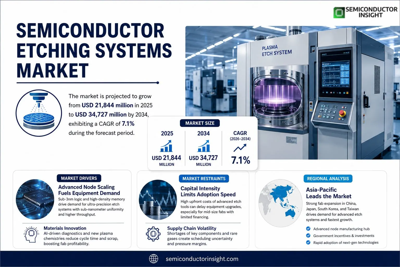
MARKET DRIVERS
Advanced Node Scaling Fuels Equipment Demand
The push toward sub‑5 nm logic and high‑density memory has intensified the need for finer etch control. Manufacturing lines now require equipment that can deliver sub‑nanometer critical dimension uniformity, prompting fab operators to upgrade to next‑generation etching platforms. Customers prioritize throughput and precision to maintain yield as design rules shrink.
Materials Innovation Expands Process Windows
Emerging high‑k dielectrics and metal‑gate stacks demand tailored plasma chemistries. Etching system vendors that integrate AI‑driven endpoint detection and real‑time plasma diagnostics are winning contracts because they reduce cycle time and scrap. This technological edge translates directly into higher fab profitability.
➤ Systems that combine modular gas delivery with adaptive recipe libraries are becoming the de‑facto standard for 3 nm and beyond.
Finally, the consolidation of major semiconductor players into integrated foundries has created a concentrated buyer base with predictable capital cycles, allowing equipment manufacturers to plan multi‑year roadmaps and invest confidently in R&D.
MARKET CHALLENGES
Capital Intensity Limits Adoption Speed
The high upfront cost of state‑of‑the‑art etching tools poses a barrier for mid‑size fabs seeking to stay competitive. Even though total cost of ownership improves over time, the initial outlay can delay equipment refresh cycles, especially in regions with constrained financing options.
Other Challenges
Supply Chain Volatility
Component shortages, particularly for rare gases and high‑purity silicon wafers, have introduced scheduling uncertainty. Vendors are forced to hold larger inventories, which erodes margins and can postpone the launch of new system generations.
MARKET RESTRAINTS
Regulatory Compliance Adds Complexity
Stringent environmental regulations governing plasma emissions and hazardous chemicals require manufacturers to incorporate additional abatement technologies. The resulting design overhead raises equipment price points and elongates development timelines, especially for suppliers targeting markets with the strictest standards.
MARKET OPPORTUNITIES
Emerging Applications in Advanced Packaging
As the industry pivots toward heterogeneous integration and chip‑let architectures, etching systems capable of processing ultra‑thin interposers and through‑silicon vias are in short supply. Vendors that can certify their tools for these novel substrates stand to capture a rapidly expanding segment of Semiconductor Etching Systems Market.
Semiconductor Etching Systems Market Trends
Advanced Node Demands Redefine Etching Capability
Manufacturers are confronting a decisive shift as the industry pushes silicon processes below the 3 nm threshold. At this scale, pattern fidelity hinges on the ability to remove material with nanometer precision while preserving vertical sidewalls. Dry‑etch platforms, which now command roughly nine‑tenths of all shipments, have responded by integrating higher‑frequency RF sources and adaptive plasma‑diagnostics. The result is a measurable lift in etch uniformity across 300 mm wafers, which directly translates into higher yields for logic and memory fabs. For equipment vendors, this translates into a premium pricing tier: high‑selectivity systems regularly command US$2.6 million per unit, reflecting the added value of tighter process windows and extended hardware lifecycles. The operational margin on these units, ranging from 38 % to 58 %, underscores the strategic importance of sustaining innovation in plasma‑source design and real‑time software control.
Other Trends
3D NAND Scaling Fuels Ultra‑High‑Aspect‑Ratio Etch
The explosion of 3D NAND capacity has placed unprecedented pressure on etch chambers to sculpt holes with aspect ratios of 60:1 to 90:1. Such geometries require plasma chemistries that can sustain ion energy deep within narrow trenches without compromising selectivity to surrounding dielectric layers. Chinese equipment producers have recently introduced a 60:1 capability that is now standard in several domestic fabs, and a 90:1 machine is slated for pilot deployment later this year. This competitive entry erodes the traditional market share of established Western suppliers and creates a new price‑performance equilibrium that will influence procurement strategies across the supply chain.
Automation and AI Integration Accelerate Throughput
Beyond raw hardware, the market is witnessing a rapid infusion of automation and AI‑driven recipe optimization. Fully automated etch systems now embed closed‑loop controllers that adjust gas flow, RF power, and chamber pressure in sub‑second intervals, effectively reducing cycle times by up to 15 %. AI‑enabled modules analyze historical run data to predict endpoint detection, minimizing scrap and extending component life. For fab operators, these capabilities translate into higher equipment utilization and lower total cost of ownership, making the technology stack increasingly attractive for both high‑volume logic fabs and niche MEMS producers. The convergence of precision hardware, sophisticated software, and data‑centric services is reshaping the competitive landscape, prompting vendors to broaden service contracts and invest heavily in field‑service analytics.
COMPETITIVE LANDSCAPE
Key Industry Players
Semiconductor Etching Systems: Competitive Overview 2025‑2034
The market is dominated by a handful of large OEMs whose product portfolios span dry‑etch platforms, plasma source modules, and advanced process‑control software. Lam Research leads with its flagship Flex family, offering high‑aspect‑ratio capabilities that underpin most 3nm logic fabs. Tokyo Electron follows closely, leveraging its strong foothold in front‑end equipment to supply multi‑wafer ICP tools prized for uniformity across 300 mm substrates. Applied Materials competes aggressively on the automation front, integrating AI‑enabled recipe optimization that shortens cycle times for memory makers. Hitachi High‑Tech rounds out the top tier, specializing in niche dielectric etch solutions that address the precise demands of 3D NAND. Collectively, these four companies command roughly 70 % of revenue, shaping pricing power and setting technology roadmaps that downstream fabs must adopt.Beyond the leaders, a diverse set of firms sustains innovation in specialized segments. SEMES supplies low‑pressure plasma sources favored for thin‑film etching in MEMS production. Oxford Instruments focuses on ultra‑high‑vacuum chambers that deliver the cleanliness required for research‑grade processes. SPTS Technologies, now part of KLA, offers metrology‑integrated etch platforms that enable real‑time defect monitoring. Plasma‑Therm targets high‑throughput wet‑etch lines for substrate prep. SAMCO and Advanced Micro‑Fabrication Equipment (AMEC) provide cost‑effective single‑wafer solutions for mid‑tier fabs. Chinese challengers NAURA Technology and GigaLane are rapidly expanding their footprint with domestic supply chains for 60:1 aspect‑ratio dielectric etch tools, positioning themselves as alternatives for cost‑sensitive foundries.
List of Key Semiconductor Etching Systems Companies Profiled
- Lam Research Corporation
- Tokyo Electron Limited
- Applied Materials, Inc.
- Hitachi High‑Tech Corporation
- SEMES Co., Ltd.
- Oxford Instruments plc
- SPTS Technologies (KLA)
- Plasma‑Therm LLC
- SAMCO Inc.
- Advanced Micro‑Fabrication Equipment Inc. (AMEC)
- NAURA Technology Group Co., Ltd.
- GigaLane Co., Ltd.
- Veeco Instruments Inc.
- Nordson MARCH
- ULVAC, Inc.
Segment Analysis:
| Segment Category | Sub-Segments | Key Insights |
| By Type |
|
Dry Etching Systems
|
| By Application |
|
Dielectric Etching
|
| By End User |
|
Pure‑Play Foundries
|
| By Automation Level |
|
AI‑Enabled Smart Etch System
|
| By Substrate Size |
|
300 mm (12‑inch) Etch System
|
Regional Analysis: Semiconductor Etching Systems Market
Asia-Pacific
As leading fabs push toward sub‑3 nm lithography, etching systems must deliver atomic‑scale precision. This pressure fuels a surge in demand for high‑aspect‑ratio etch tools, prompting OEMs to prioritize plasma chemistry innovations that sustain yield while minimizing defectivity.
National chip initiatives in China, South Korea, and Taiwan allocate substantial subsidies toward equipment procurement. These programmes lower total cost of ownership for end users, accelerating the refresh cycle of etch platforms across the region.
Proximity between equipment makers and fabs shortens feedback loops, enabling rapid firmware updates and parts‑on‑demand logistics. This tight integration reduces lead times and cushions the market against component shortages.
Japanese and Korean OEMs vie with emerging Taiwanese vendors for market share. The rivalry pushes each player to differentiate via cycle‑time reductions, energy‑efficient plasma sources, and service‑first business models.
North America
In North America, Semiconductor Etching Systems Market is shaped by a focus on advanced research, defense‑related production, and a resurgence of domestic fab investment. Federal incentives aimed at reshoring chip manufacturing have spurred early‑stage capacity additions, prompting equipment suppliers to tailor solutions for high‑mix, low‑volume environments. Collaborative programs between universities and OEMs nurture next‑generation etch chemistries, while a mature services sector emphasizes predictive maintenance to extend tool life. These dynamics encourage a steady, albeit more measured, growth trajectory compared with the pace observed in Asia‑Pacific.
Europe
European stakeholders prioritize sustainability and precision in etching processes, aligning with the EU’s broader green‑technology agenda. Leading foundries in Germany and the Netherlands are exploring low‑power plasma sources that reduce carbon footprints without compromising performance. Regulatory frameworks push OEMs to certify equipment for hazardous‑material handling, fostering a niche for environmentally‑optimized solutions. Moreover, the region’s strong emphasis on standardization influences tool specifications, positioning Europe as a subtle driver of industry best practices.
South America
South America remains a modest participant in Semiconductor Etching Systems Market, with activity concentrated around Brazil’s nascent fab projects. Limited domestic demand forces regional players to rely on service contracts and retrofit programs for older generations of equipment. Nonetheless, growing interest from governmental bodies in establishing a semiconductor ecosystem creates a longer‑term incentive for technology transfer and skill development, suggesting a gradual, opportunity‑rich entry point for equipment vendors willing to invest in local partnerships.
Middle East & Africa
The Middle East & Africa region is at an early stage of semiconductor infrastructure development. Strategic plans in Saudi Arabia and the United Arab Emirates envision full‑scale fabs within the next decade, prompting OEMs to conduct feasibility studies and pilot deployments. While current market volume is limited, the prospect of establishing a regional supply hub attracts equipment manufacturers seeking first‑mover advantages. Success will hinge on aligning with national investment programmes and nurturing a local talent pool capable of supporting sophisticated etch platforms.
Report Scope
This market research report provides a comprehensive analysis of the Semiconductor Etching Systems Market , covering the forecast period 2026–2034. It offers detailed insights into market dynamics, technological advancements, competitive landscape, and key trends shaping the industry.
Key focus areas of the report include:
- Market Overview: The report begins with an overview outlining its current market scenario, key growth indicators, and industry transformation drivers. It discusses macroeconomic factors, demand–supply balance, regulatory landscape, and the strategic role of semiconductors in powering advancements across industries such as automotive, telecommunications, consumer electronics, and industrial automation.
- Market Size & Forecast: Historical data and future projections for revenue, unit shipments, and market value across major regions and segments.
- Segmentation Analysis: Detailed breakdown by product type, technology, application, and end-user industry to identify high-growth segments and investment opportunities.
- Regional Insights: Insights into market performance across North America, Europe, Asia-Pacific, Latin America, and the Middle East & Africa, including country-level analysis where relevant.
- Competitive Landscape: Profiles of leading market participants, including their product offerings, R&D focus, manufacturing capacity, pricing strategies, and recent developments such as mergers, acquisitions, and partnerships.
- Technology Trends & Innovation: Assessment of emerging technologies, integration of AI/IoT, semiconductor design trends, fabrication techniques, and evolving industry standards.
- Market Drivers & Restraints: Evaluation of factors driving market growth along with challenges, supply chain constraints, regulatory issues, and market-entry barriers.
- Stakeholder Insights: Insights for component suppliers, OEMs, system integrators, investors, and policymakers regarding the evolving ecosystem and strategic opportunities.
Primary and secondary research methods are employed, including interviews with industry experts, data from verified sources, and real-time market intelligence to ensure the accuracy and reliability of the insights presented.
FREQUENTLY ASKED QUESTIONS:
What is the current market size of Semiconductor Etching Systems Market?
-> Semiconductor Etching Systems Market was valued at USD 21,844 million in 2025 and is expected to reach USD 34,727 million by 2034, growing at a CAGR of 7.1% during the forecast period.
Which key companies operate in Semiconductor Etching Systems Market?
-> Key players include Lam Research Corporation, Tokyo Electron Limited (TEL), Applied Materials, Inc., Hitachi High‑Tech Corporation, SEMES Co., Ltd., Oxford Instruments plc, SPTS Technologies (KLA), Plasma‑Therm LLC, SAMCO Inc., Advanced Micro‑Fabrication Equipment Inc. (AMEC), NAURA Technology Group Co., Ltd., and GigaLane Co., Ltd.
What are the key growth drivers?
-> Key growth drivers include the industry’s push toward sub‑3 nm nodes, increasing demand for high‑density 3D NAND flash, the transition to FinFET and gate‑all‑around architectures, and the need for ultra‑high‑aspect‑ratio etching capabilities.
Which region dominates the market?
-> Asia is the dominant region, driven by strong manufacturing activity in China, Japan, South Korea, and Taiwan, while also showing the fastest growth rate.
What are the emerging trends?
-> Emerging trends include AI‑enabled smart etch systems, increased automation and fully‑automated solutions, and the development of equipment capable of ultra‑high aspect‑ratio (60:1 to 90:1) dielectric etching for advanced 3D NAND applications.
Get Sample Report PDF for Exclusive Insights
Report Sample Includes
- Table of Contents
- List of Tables & Figures
- Charts, Research Methodology, and more...
 Download Sample Report PDF