MARKET INSIGHTS
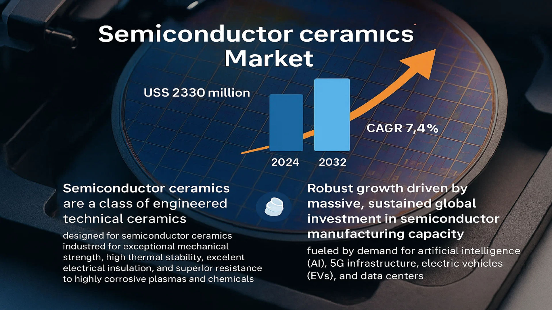
The global Semiconductor Ceramics Market was valued at 2330 million in 2024 and is projected to reach US$ 4098 million by 2032, at a CAGR of 7.4% during the forecast period.
Semiconductor ceramics are a class of engineered technical ceramics specifically designed for use in semiconductor manufacturing equipment and processes. These advanced materials are critical structural components within fabrication tools, prized for their exceptional mechanical strength, high thermal stability, excellent electrical insulation, and superior resistance to highly corrosive plasmas and chemicals. They are integral to numerous applications, including wafer handling, deposition (CVD, PVD, ALD), etching, ion implantation, and chemical mechanical planarization (CMP).
The market’s robust growth is primarily driven by the massive, sustained global investment in semiconductor manufacturing capacity, fueled by demand for artificial intelligence (AI), 5G infrastructure, electric vehicles (EVs), and data centers. Because these ceramics are essential for producing the most advanced chips, their demand directly correlates with capital expenditure in new fabrication plants (fabs). Furthermore, the market is highly consolidated, with the top seven players holding over 80% of the global market share as of 2024. Key established players such as NGK Insulators, Kyocera, and CoorsTek continue to strengthen their positions through strategic expansions and acquisitions.
MARKET DYNAMICS
MARKET DRIVERS
Escalating Semiconductor Demand Across Key Industries to Propel Market Expansion
The global semiconductor ceramics market is experiencing robust growth driven by unprecedented demand across multiple high-growth sectors. The proliferation of artificial intelligence, 5G infrastructure, electric vehicles, and data centers has created an insatiable need for advanced semiconductor components. Global semiconductor equipment spending reached approximately $109 billion in 2024, representing a significant increase from previous years, with projections indicating continued expansion. This substantial capital investment directly translates to increased demand for ceramic components used in semiconductor manufacturing equipment. The exceptional material properties of technical ceramics—including superior thermal conductivity, excellent mechanical strength, and remarkable chemical stability—make them indispensable in harsh semiconductor fabrication environments where they withstand extreme temperatures, corrosive gases, and plasma exposure.
Advancements in Semiconductor Manufacturing Technologies to Accelerate Adoption
Technological evolution in semiconductor manufacturing processes continues to drive ceramic component innovation and adoption. The transition to smaller process nodes below 5 nanometers requires increasingly sophisticated equipment with higher precision and stability, creating greater reliance on advanced ceramic materials. Semiconductor ceramics enable critical processes including chemical vapor deposition, etching, ion implantation, and chemical mechanical planarization by providing exceptional dimensional stability, minimal particle generation, and superior contamination control. The development of new ceramic compositions and manufacturing techniques has enabled components to withstand higher processing temperatures exceeding 1,200°C while maintaining structural integrity and thermal shock resistance. These material advancements are essential for next-generation semiconductor manufacturing where process temperatures continue to increase while feature sizes decrease.
Furthermore, the expansion of compound semiconductor manufacturing for power electronics and RF applications has created additional demand for specialized ceramic components capable of handling gallium nitride and silicon carbide processing requirements.
➤ For instance, the implementation of atomic layer deposition technology requires ceramic components with exceptional surface finish and purity levels below 1 part per million contamination, driving innovation in advanced ceramic manufacturing processes.
The continuous push toward higher wafer throughput and larger wafer sizes, including the transition to 450mm wafer processing, necessitates ceramic components with enhanced mechanical properties and larger dimensions, further stimulating market growth through technological advancement.
MARKET RESTRAINTS
High Manufacturing Costs and Complex Production Processes to Limit Market Penetration
The semiconductor ceramics market faces significant constraints due to the substantial costs associated with advanced ceramic manufacturing. The production of high-purity ceramic components requires specialized raw materials, energy-intensive sintering processes, and precision machining capabilities that contribute to elevated manufacturing expenses. Technical ceramics for semiconductor applications often require purity levels exceeding 99.9% with controlled grain structures and minimal porosity, necessitating sophisticated manufacturing techniques and rigorous quality control measures. The capital investment for establishing semiconductor-grade ceramic production facilities can reach hundreds of millions of dollars, creating high barriers to entry and limiting market participation to established players with substantial financial resources.
Additionally, the lengthy development cycles for new ceramic formulations and the complexity of scaling production while maintaining consistent quality present significant challenges for market expansion. The certification process for semiconductor ceramic components typically requires extensive testing and validation that can extend over multiple quarters, delaying time-to-market and increasing development costs.
Technical Limitations in Ceramic Properties to Hinder Application Scope
While semiconductor ceramics offer exceptional material properties, certain technical limitations restrict their application in emerging semiconductor manufacturing processes. The inherent brittleness of ceramic materials presents challenges in applications requiring impact resistance or complex geometries. Thermal expansion mismatch between ceramics and other materials used in semiconductor equipment can lead to structural failures under thermal cycling conditions. Furthermore, achieving the required surface finish for advanced lithography applications often necessitates additional processing steps that increase costs and manufacturing complexity. The development of ceramic components for extreme ultraviolet lithography systems requires surface roughness specifications below 0.5 nanometers, pushing the limits of current ceramic manufacturing capabilities.
These technical constraints necessitate ongoing research and development efforts to improve ceramic material properties, but they currently present significant barriers to more widespread adoption in the most advanced semiconductor manufacturing applications.
MARKET CHALLENGES
Supply Chain Vulnerabilities and Raw Material Availability to Challenge Market Stability
The semiconductor ceramics industry faces considerable challenges related to supply chain resilience and raw material sourcing. The market depends on consistent access to high-purity raw materials including aluminum oxide, aluminum nitride, silicon carbide, and silicon nitride, with specific quality requirements that limit the number of qualified suppliers. Geopolitical tensions and trade restrictions have created uncertainty in the supply of critical raw materials, particularly those sourced from limited geographical regions. The concentration of advanced ceramic manufacturing capabilities in specific regions creates additional supply chain vulnerabilities, as demonstrated during recent global disruptions where lead times for ceramic components extended beyond 12 months in some cases.
Other Challenges
Technical Expertise Shortage
The industry faces a significant shortage of skilled professionals with expertise in advanced ceramic technology and semiconductor applications. The specialized knowledge required for developing and manufacturing semiconductor-grade ceramics includes materials science, precision engineering, and semiconductor process understanding. The aging workforce in established ceramic manufacturing regions compounds this challenge, as experienced technicians and engineers approach retirement without adequate knowledge transfer to younger generations.
Rapid Technological Obsolescence
The accelerated pace of semiconductor technology advancement creates challenges for ceramic component manufacturers who must continuously innovate to meet evolving requirements. Components developed for current-generation semiconductor equipment may become obsolete within 2-3 years as process technologies advance, requiring constant research and development investment to maintain market relevance.
MARKET OPPORTUNITIES
Emerging Applications in Advanced Packaging and Heterogeneous Integration to Create Growth Prospects
The semiconductor ceramics market stands to benefit significantly from the growing adoption of advanced packaging technologies and heterogeneous integration approaches. The increasing complexity of semiconductor devices, particularly for artificial intelligence and high-performance computing applications, requires sophisticated packaging solutions where ceramic substrates and components play crucial roles. Ceramic materials enable thermal management, signal integrity, and reliability in 2.5D and 3D packaging configurations that are becoming essential for next-generation semiconductor devices. The market for advanced semiconductor packaging is projected to grow at approximately 8% annually, creating substantial opportunities for ceramic component manufacturers specializing in substrates, interposers, and thermal management solutions.
Geographical Expansion and Localization Initiatives to Unlock New Market Potential
Substantial opportunities exist in the ongoing geographical diversification of semiconductor manufacturing capabilities, particularly with the establishment of new fabrication facilities across multiple regions. Major semiconductor manufacturers are investing over $500 billion in new manufacturing capacity globally through 2030, with significant projects underway in North America, Europe, and Southeast Asia. This geographical expansion creates opportunities for ceramic component suppliers to establish local manufacturing and support facilities near new semiconductor clusters. Additionally, government initiatives promoting semiconductor supply chain resilience and localization provide incentives for ceramic manufacturers to establish production capabilities in regions previously dependent on imports.
The development of regional semiconductor ecosystems, particularly in areas with growing technological capabilities, presents opportunities for ceramic component manufacturers to participate in emerging supply chains and establish long-term partnerships with new semiconductor fabrication facilities.
SEMICONDUCTOR CERAMICS MARKET TRENDS
Accelerated Demand from Advanced Semiconductor Fabrication Processes
The relentless push towards smaller process nodes, particularly below 5nm, is fundamentally reshaping the requirements for materials used in semiconductor manufacturing equipment. This trend is creating unprecedented demand for high-purity, ultra-stable semiconductor ceramics that can withstand increasingly aggressive processing environments. Components fabricated from materials like Aluminum Nitride (AlN) and Silicon Carbide (SiC) are essential in chambers for processes such as Atomic Layer Deposition (ALD) and plasma etching, where their exceptional thermal conductivity, corrosion resistance, and electrical insulation properties are non-negotiable. The transition to extreme ultraviolet (EUV) lithography has further intensified this demand, as the ceramic stages and chucks used in these multi-million-dollar machines must maintain nanometer-level flatness and stability under intense heat loads. This technological arms race directly fuels market growth, with the global semiconductor ceramics market projected to grow from its 2024 valuation of $2330 million to over $4098 million by 2032, representing a compound annual growth rate of 7.4%. This growth is intrinsically linked to the capital expenditure of semiconductor manufacturers, which exceeded $190 billion in 2023 alone, a significant portion of which is allocated to advanced equipment requiring these critical ceramic components.
Other Trends
Geopolitical Reshoring and Supply Chain Diversification
Intensifying geopolitical tensions and a strategic focus on supply chain security are compelling nations to invest heavily in domestic semiconductor production capabilities. Major initiatives like the U.S. CHIPS and Science Act and the European Chips Act are channeling hundreds of billions of dollars into new fab construction and modernization. This wave of investment is a powerful catalyst for the semiconductor ceramics market, as every new fabrication facility requires a complete suite of equipment loaded with ceramic components. This trend is most pronounced in regions like North America and Europe, which are actively seeking to reduce their reliance on Asian supply chains. However, it also presents a significant challenge: the market is currently dominated by a handful of established players, primarily from Japan and the United States, who collectively hold over 80% of the market share. This concentration creates a potential bottleneck, driving new entrants, particularly in China, to rapidly develop and scale their production of high-performance ceramics to support their own growing domestic semiconductor industry, which is expected to grow at a CAGR of 10.69% between 2025 and 2030.
Material Innovation for Next-Generation Applications
Beyond traditional silicon-based semiconductors, the rise of new applications is driving innovation in ceramic material science. The explosive growth in markets for Electric Vehicles (EVs), 5G infrastructure, and Artificial Intelligence (AI) data centers is creating massive demand for power semiconductors and radio-frequency (RF) chips based on wide-bandgap materials like Gallium Nitride (GaN) and Silicon Carbide (SiC). The fabrication of these devices often requires even higher processing temperatures and more corrosive environments than standard silicon, necessitating the development of next-generation ceramic components that offer superior performance. For instance, ceramic heaters and susceptors used in the Metal-Organic Chemical Vapor Deposition (MOCVD) of GaN layers must exhibit exceptional purity and thermal shock resistance. Furthermore, in the packaging phase, ceramic substrates are critical for providing the necessary thermal management and electrical isolation for high-power modules. This shift is prompting material suppliers to invest heavily in R&D to create advanced composite ceramics and refined manufacturing processes to meet these stringent new requirements, ensuring their components can handle the thermal and mechanical stresses of tomorrow’s semiconductor technologies.
COMPETITIVE LANDSCAPE
Key Industry Players
Market Leaders Leverage Material Expertise and Strategic Expansion to Maintain Dominance
The global semiconductor ceramics market exhibits a semi-consolidated structure, characterized by the presence of a few dominant international players alongside numerous regional and specialized manufacturers. NGK Insulators, Ltd. stands as a preeminent force, commanding a significant market share due to its extensive portfolio of high-purity alumina and aluminum nitride components and its deeply entrenched relationships with major semiconductor equipment OEMs across Asia and North America.
Kyocera Corporation and CoorsTek, Inc. are also pivotal players, holding substantial market positions. Their leadership is largely attributed to decades of ceramic engineering experience, vertically integrated manufacturing capabilities, and a relentless focus on research and development to meet the extreme purity and performance requirements of advanced node semiconductor fabrication.
These established giants are actively strengthening their market positions through strategic capacity expansions and acquisitions. For instance, recent investments in new production facilities, particularly in Southeast Asia, are aimed at catering to the growing regional demand and securing supply chain resilience. Such growth initiatives are anticipated to further consolidate their collective market share in the coming years.
Meanwhile, other key players like Morgan Advanced Materials and Ferrotec Corporation are bolstering their competitive stance through significant R&D investments in novel material compositions and advanced manufacturing techniques, such as additive manufacturing for complex ceramic parts. Their strategy focuses on developing solutions for next-generation applications in Etch, CVD, and wafer handling equipment, ensuring their relevance in an evolving technological landscape.
The competitive dynamics are further influenced by the rapid emergence of Chinese manufacturers. Companies such as Hebei Sinopack Electronic Technology and ChaoZhou Three-circle are expanding their capabilities and competing aggressively on cost, gradually capturing share in the domestic market and increasingly on a global scale.
List of Key Semiconductor Ceramics Companies Profiled
- NGK Insulators, Ltd. (Japan)
- Kyocera Corporation (Japan)
- CoorsTek, Inc. (U.S.)
- Ferrotec Corporation (Japan)
- TOTO Advanced Ceramics (Japan)
- Morgan Advanced Materials (U.K.)
- CeramTec GmbH (Germany)
- Saint-Gobain (France)
- MiCo Ceramics Co., Ltd. (South Korea)
- Niterra Co., Ltd. (Japan)
- Suzhou KemaTek, Inc. (China)
Segment Analysis:
By Type
Alumina Ceramics Segment Dominates Due to Excellent Mechanical Stability and Cost-Effectiveness
The market is segmented based on type into:
- Alumina Ceramics
- AlN Ceramics
- SiC Ceramics
- Si3N4 Ceramics
- Others
By Application
Semiconductor Deposition Equipment Segment Leads Due to Critical Role in Chip Fabrication Processes
The market is segmented based on application into:
- Semiconductor Deposition Equipment
- Semiconductor Etch Equipment
- Lithography Machines
- Ion Implant Equipment
- Heat Treatment Equipment
- CMP Equipment
- Wafer Handling
- Assembly Equipment
- Others
By Material Property
High Thermal Conductivity Materials Gain Traction for Advanced Heat Dissipation Applications
The market is segmented based on material property into:
- High Thermal Conductivity Ceramics
- High Mechanical Strength Ceramics
- Corrosion Resistant Ceramics
- Electrical Insulating Ceramics
- Others
By End-User
Foundries Segment Leads Owing to Massive Semiconductor Manufacturing Requirements
The market is segmented based on end-user into:
- Semiconductor Foundries
- IDM (Integrated Device Manufacturers)
- Semiconductor Equipment Manufacturers
- Research and Development Institutes
- Others
Regional Analysis: Semiconductor Ceramics Market
Asia-Pacific
The Asia-Pacific region is the undisputed leader in the global semiconductor ceramics market, driven by its position as the world’s manufacturing hub for semiconductors. This dominance is fueled by massive investments in new fabrication plants (fabs), particularly in China, Taiwan, South Korea, and Japan. China is projected to be the fastest-growing market, with a forecasted CAGR of 10.69% from 2025 to 2030, propelled by aggressive government initiatives aimed at achieving semiconductor self-sufficiency. The region accounts for the highest volume consumption of semiconductor ceramics, with key applications spanning deposition equipment, etch equipment, and CMP equipment. While global giants like Kyocera (Japan), NGK Insulators (Japan), and TOTO Advanced Ceramics (Japan) maintain a stronghold, a vibrant ecosystem of local players is emerging, including Suzhou KemaTek, Inc. (China) and Ferrotec (China). The relentless demand for chips from the consumer electronics, automotive (especially EVs), and AI sectors continues to be the primary growth engine.
North America
North America is a technologically advanced and innovation-centric market for semiconductor ceramics, characterized by the presence of leading semiconductor equipment manufacturers and fabless chip design companies. The region’s growth is underpinned by substantial government support, such as the U.S. CHIPS and Science Act, which allocates billions in funding to bolster domestic semiconductor research, development, and manufacturing. This policy-driven investment is creating a robust demand for high-performance, precision ceramic components used in advanced lithography machines, ion implant equipment, and wafer handling systems. Key players operating in this region include U.S.-based companies like Coorstek and 3M, who supply critical components to major equipment OEMs. The focus is intensely on developing next-generation ceramics that can withstand the extreme conditions of sub-5nm and 3nm process nodes, with a strong emphasis on material purity and thermal management properties.
Europe
Europe maintains a significant and specialized presence in the semiconductor ceramics market, anchored by strong technical expertise and a focus on high-value, niche applications. The region is home to several leading research institutions and manufacturers that excel in producing advanced ceramic materials, particularly for extreme environments. Key applications include components for heat treatment equipment and assembly tools, where mechanical integrity and thermal stability are paramount. European companies like CeramTec (Germany) and Morgan Advanced Materials (UK) are recognized for their innovation in materials such as silicon nitride (Si3N4) and aluminum nitride (AlN). Growth is further supported by the EU’s broader digital and green industrial strategies, which aim to strengthen the region’s technological sovereignty. However, the market’s expansion is more measured compared to Asia-Pacific, focusing on quality and specialization over volume.
South America
The semiconductor ceramics market in South America is in a nascent stage of development. The region’s involvement in the global semiconductor supply chain is currently limited, with minimal local semiconductor fabrication capacity. Consequently, the demand for high-performance semiconductor ceramics is correspondingly low and is primarily met through imports. The market is largely confined to supporting maintenance, repair, and operations (MRO) activities for existing industrial and electronics manufacturing equipment. Countries like Brazil and Argentina have nascent electronics sectors, but economic volatility and a lack of significant investment in high-tech manufacturing infrastructure hinder the development of a local market for these specialized components. Long-term growth is potential is tied to broader economic stabilization and strategic investments in technology industrialization.
Middle East & Africa
The market for semiconductor ceramics in the Middle East & Africa is emerging but remains highly underdeveloped. The region has very limited semiconductor manufacturing footprint, which is the primary driver for ceramic component demand. Current consumption is almost entirely for imported electronics and industrial equipment that require ceramic parts for operation. Select nations in the Middle East, such as Saudi Arabia and the UAE, are launching ambitious economic diversification plans (e.g., Saudi Vision 2030) that include developing advanced technological sectors. While these initiatives may foster a future electronics manufacturing ecosystem, the demand for semiconductor ceramics is projected to remain negligible in the short to medium term. The market’s progression is intrinsically linked to the success of these long-term, large-scale national transformation projects.
Report Scope
This market research report provides a comprehensive analysis of the global and regional Semiconductor Ceramics markets, covering the forecast period 2025–2032. It offers detailed insights into market dynamics, technological advancements, competitive landscape, and key trends shaping the industry.
Key focus areas of the report include:
- Market Size & Forecast: Historical data and future projections for revenue, unit shipments, and market value across major regions and segments.
- Segmentation Analysis: Detailed breakdown by product type, technology, application, and end-user industry to identify high-growth segments and investment opportunities.
- Regional Outlook: Insights into market performance across North America, Europe, Asia-Pacific, Latin America, and the Middle East & Africa, including country-level analysis where relevant.
- Competitive Landscape: Profiles of leading market participants, including their product offerings, R&D focus, manufacturing capacity, pricing strategies, and recent developments such as mergers, acquisitions, and partnerships.
- Technology Trends & Innovation: Assessment of emerging technologies, integration of AI/IoT, semiconductor design trends, fabrication techniques, and evolving industry standards.
- Market Drivers & Restraints: Evaluation of factors driving market growth along with challenges, supply chain constraints, regulatory issues, and market-entry barriers.
- Stakeholder Analysis: Insights for component suppliers, OEMs, system integrators, investors, and policymakers regarding the evolving ecosystem and strategic opportunities.
Primary and secondary research methods are employed, including interviews with industry experts, data from verified sources, and real-time market intelligence to ensure the accuracy and reliability of the insights presented.
FREQUENTLY ASKED QUESTIONS:
What is the current market size of Global Semiconductor Ceramics Market?
-> Semiconductor Ceramics Market was valued at 2330 million in 2024 and is projected to reach US$ 4098 million by 2032, at a CAGR of 7.4% during the forecast period.
Which key companies operate in Global Semiconductor Ceramics Market?
-> Key players include NGK Insulators, Kyocera, Coorstek, Ferrotec, TOTO Advanced Ceramics, Morgan Advanced Materials, and Niterra Co., Ltd., among others. The top seven players hold a combined market share of over 80%.
What are the key growth drivers?
-> Key growth drivers include rising investments in semiconductor fabrication equipment, expansion of data centers, proliferation of Electric Vehicles (EVs), 5G infrastructure deployment, and advancements in AI technologies.
Which region dominates the market?
-> Asia-Pacific is the largest and fastest-growing market, with China expected to grow at a CAGR of 10.69% from 2025 to 2030.
What are the emerging trends?
-> Emerging trends include increased adoption of Aluminum Nitride (AlN) ceramics for high thermal conductivity applications, development of advanced ceramic composites, and expansion of local manufacturing capabilities in China.

Get Sample Report PDF for Exclusive Insights
Report Sample Includes
- Table of Contents
- List of Tables & Figures
- Charts, Research Methodology, and more...