
Reticle Mask Particle Detection Systems Market Insights
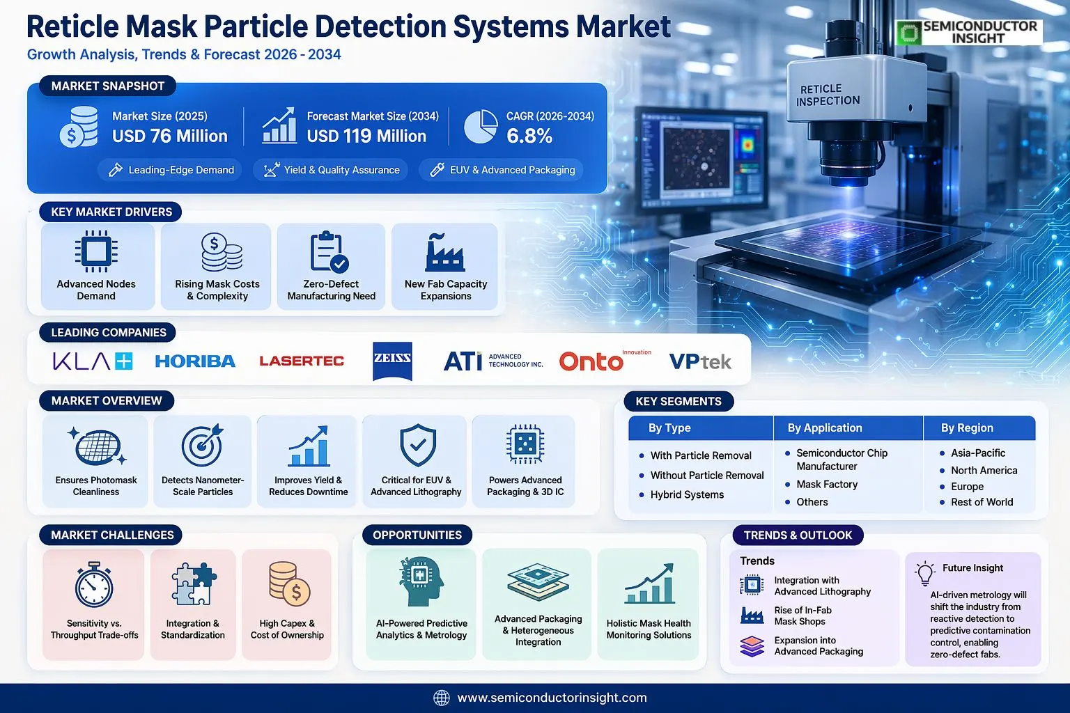
Global Reticle Mask Particle Detection Systems market size was valued at USD 76 million in 2025. The market is projected to grow from USD 81.3 million in 2026 to USD 119 million by 2034, exhibiting a CAGR of 6.8% during the forecast period.
Reticle Mask Particle Detection Systems are critical metrology tools used in semiconductor manufacturing to ensure the quality and cleanliness of photomasks, which are also known as reticles. These systems detect and analyze microscopic particles, defects, and contamination on the mask surface that can be replicated onto silicon wafers during the lithography process, thereby helping to maintain high production yield and device reliability. The technology is essential for advanced nodes where even nanometer-scale defects can cause catastrophic chip failures.
The market growth is primarily driven by the relentless push for smaller semiconductor geometries and the increasing complexity of chip designs, which demand stricter defect control. Furthermore, the expansion of fabrication capacity globally, particularly for leading-edge logic and memory chips, necessitates more inspection tools. Key industry players are actively advancing their technologies; for instance, KLA Corporation continuously enhances its TeraScan platform for faster, more sensitive mask inspection. Other significant manufacturers operating in this specialized market include Lasertec Corporation, HORIBA, and Carl Zeiss AG.
MARKET DRIVERS
Relentless Demand for Advanced Semiconductor Nodes
The persistent industry push beyond 5nm process technologies is a primary driver for the Reticle Mask Particle Detection Systems Market. At these extreme nodes, a single contaminant particle can render a photomask unusable, potentially causing significant yield loss. This makes in-pod and pellicle particle detection systems, which monitor reticle cleanliness in real-time within lithography scanners, a critical component of advanced manufacturing lines to ensure zero-defect production.
Rising Complexity and Cost of Photomasks
As photomasks for leading-edge logic and memory become exceedingly complex and expensive, with costs exceeding $1 million per set, the financial imperative to protect this intellectual property and capital investment intensifies. Implementing robust Reticle Mask Particle Detection Systems is essential to prevent costly reworks and scrapping of these critical assets, directly supporting fab operational economics and return on investment.
➤ The integration of these detection systems is now a baseline requirement in new fab construction and technology qualification phases for major foundries.
Furthermore, the industry’s strategic expansion, including significant new fab construction globally, mandates the adoption of best-in-class contamination control. This capital expenditure wave directly fuels the procurement and integration of advanced particle detection and monitoring solutions across the semiconductor supply chain.
MARKET CHALLENGES
Sensitivity Versus Throughput Trade-offs
A core technical challenge within the Reticle Mask Particle Detection Systems Market is balancing ultra-high sensitivity, required to detect nanometer-scale particles, with the need for high-speed, in-line inspection that does not impede scanner throughput. Developing detection technologies that achieve sub-50nm sensitivity at production-line speeds remains an ongoing engineering effort, with system calibration and stability posing significant hurdles.
Other Challenges
Integration and Standardization
Integrating disparate detection systems from different vendors into a cohesive fab-wide monitoring network is complex. The lack of universal communication protocols and data formats between equipment from lithography scanner manufacturers, detection system providers, and factory automation systems can create data silos and reduce overall effectiveness.
Cost of Ownership and False Positives
The total cost of ownership for these sophisticated systems is a consideration. This includes not only the initial capital outlay but also maintenance, consumables, and the operational impact of managing false-positive detections, which can trigger unnecessary reticle handling and cleaning cycles, introducing risk and downtime.
MARKET RESTRAINTS
High Capital Intensity and Cyclical Industry Downturns
The capital-intensive nature of semiconductor manufacturing acts as a significant restraint. During periods of industry downturn or reduced capital expenditure, fabs may delay or cancel investments in ancillary equipment, including upgrades for reticle inspection and particle detection systems, prioritizing spending on core lithography tools.
Technological Saturation at Mature Nodes
A considerable portion of global semiconductor production still utilizes mature process nodes (>28nm), where the tolerance for particle contamination is less stringent. Manufacturers in these segments often perceive the return on investment for the latest high-sensitivity particle detection systems as insufficient, slowing adoption outside of leading-edge logic and memory fabs.
Additionally, the development cycle for next-generation detection technology is long and R&D-heavy. This creates a lag between the identification of new contamination challenges at the research level and the availability of commercially robust, qualified solutions for the production floor.
MARKET OPPORTUNITIES
Expansion into Advanced Packaging and Heterogeneous Integration
The rapid growth of advanced packaging schemes, such as 2.5D/3D integration and chiplet-based designs, presents a substantial growth vector. These processes involve handling and lithography on reconstituted wafers and interposers, which are also susceptible to yield-limiting particles, creating a parallel demand for specialized particle detection systems tailored to these new manufacturing flows.
AI-Powered Predictive Analytics and Metrology
The integration of artificial intelligence and machine learning with detection system data offers a transformative opportunity. By analyzing historical and real-time particle maps, AI can shift the paradigm from reactive detection to predictive contamination control, identifying patterns that forecast particle generation events before they impact yield, thereby enabling preventative maintenance and smarter cleanroom management.
Furthermore, the increasing need for comprehensive process control and traceability is driving opportunities for system vendors to offer holistic monitoring suites. These solutions combine particle detection with other reticle metrology data, providing fabs with a complete digital twin of their mask health for superior process optimization and yield ramp.
Reticle Mask Particle Detection Systems Market Trends
Integration with Advanced Lithography for Shrinking Nodes
The drive toward more advanced semiconductor nodes is a primary trend shaping the Reticle Mask Particle Detection Systems market. As feature sizes shrink to 3nm and below, the tolerance for particulate contamination on a photomask approaches zero. This necessitates detection systems with significantly higher sensitivity, capable of identifying particles as small as several tens of nanometers. Consequently, leading manufacturers are innovating with more powerful light sources, higher-resolution optics, and sophisticated algorithms to differentiate between critical defects and non-critical anomalies. The integration of these systems directly with lithography tool workflows is becoming standard to enable real-time monitoring and faster corrective actions, directly impacting fab yield and throughput.
Other Trends
Rise of In-Fab Mask Shops
A growing trend is the establishment of sophisticated in-fab mask shops by major semiconductor chip manufacturers. This vertical integration reduces dependency on external mask suppliers and shortens the cycle time for critical mask development and qualification. In such environments, Reticle Mask Particle Detection Systems are crucial for ensuring mask integrity before and after each wafer exposure. This trend increases demand for systems offering high throughput and automated, trackable reporting to maintain stringent in-fab contamination control protocols and meet just-in-time manufacturing schedules.
Expansion into Advanced Packaging Applications
Beyond front-end lithography, Reticle Mask Particle Detection Systems are seeing increased application in advanced packaging technologies, such as fan-out wafer-level packaging and 2.5D/3D integration. The photomasks used in these processes, while often featuring larger geometries than leading-edge logic, require high reliability and freedom from catastrophic defects. Systems originally designed for semiconductor front-end use are being adapted and deployed in packaging facilities to ensure quality. This diversification represents a growth segment for market players, driven by the push for heterogeneous integration and improved device performance beyond Moore’s Law scaling.
COMPETITIVE LANDSCAPE
Key Industry Players
Market Leadership Anchored in Yield Management Solutions for Advanced Semiconductor Node Production
Global Reticle Mask Particle Detection Systems market is characterized by a high degree of technological concentration. KLA Corporation stands as the predominant leader, leveraging its comprehensive suite of process control and yield management solutions to secure a significant market share. This dominance is built on deep integration with semiconductor fabrication workflows and a strong presence in leading-edge logic and memory fabs, where defect control is paramount. The overall market structure is oligopolistic, with the top five players accounting for a substantial portion of global revenue, driven by continuous R&D investment to keep pace with shrinking design rules and the transition to EUV lithography.
Beyond the leading incumbents, several key players maintain strong positions by focusing on specialized technologies or regional markets. Companies like Lasertec Corporation are critical for EUV mask blank inspection, while HORIBA and Carl Zeiss (Zeiss) offer advanced optical and analytical solutions integral to contamination analysis. Niche innovators and regional specialists, such as Korea’s Advanced Technology Inc. (ATI) and Taiwan’s VPTek, address specific application needs and provide competitive alternatives in the mask shop and foundry segments, fostering a competitive environment for performance, precision, and cost-effectiveness in particle detection.
List of Key Reticle Mask Particle Detection Systems Companies Profiled
- KLA Corporation
- HORIBA, Ltd.
- Lasertec Corporation
- Advanced Technology Inc. (ATI)
- Carl Zeiss AG
- Fastmicro
- LAZIN
- VPTek
- Applied Materials, Inc.
- Onto Innovation Inc.
- Hitachi High-Tech Corporation
- ASML (HMI)
- Plasma-Therm LLC
- Rudolph Technologies, Inc.
- Nanometrics (now part of Onto Innovation)
Segment Analysis:
| Segment Category | Sub-Segments | Key Insights |
| By Type |
|
With Particle Removal systems represent a more advanced and value-added solution that is increasingly favored for ensuring mask integrity. These integrated systems not only identify contaminants but also cleanse the reticle, which is a critical advantage for high-volume manufacturing where downtime is costly. Their adoption is driven by the demand for higher process automation and yield assurance in cutting-edge node production. The ability to combine detection and remediation in a single tool reduces the risk of handling damage and aligns with the industry’s push towards more comprehensive in-line metrology and process control solutions. |
| By Application |
|
Semiconductor Chip Manufacturer is the predominant application segment due to the critical need for in-fab mask quality control. As chipmakers pursue smaller process nodes, the tolerance for particulate contamination on reticles shrinks exponentially, making robust detection systems indispensable for maintaining yield. These manufacturers invest heavily in such systems to perform regular inspections during the lithography process, preventing costly wafer reworks. The integration of detection systems into the fab’s overall equipment effectiveness strategy is a key trend, emphasizing their role not just as inspection tools but as essential components of the yield management ecosystem. |
| By End User |
|
Foundries constitute a leading and highly demanding end-user segment, driven by their service model which requires guaranteeing process integrity for diverse client designs. The competitive pressure to offer superior yield rates to fabless semiconductor companies compels foundries to adopt the most advanced detection technologies. Their high-volume, multi-product manufacturing environment creates a continuous need for monitoring mask cleanliness across numerous lithography steps. Consequently, foundries often pioneer the adoption of integrated detection and removal systems, seeking to minimize cross-contamination risks and ensure consistent quality output for their global customer base. |
| By Technology |
|
Hybrid Systems are emerging as a sophisticated solution that combines multiple detection methodologies for superior accuracy and defect classification. By integrating laser scattering for rapid, sensitive particle detection with high-resolution image analysis for defect characterization, these systems provide a more complete picture of mask contamination. This technological convergence is crucial for identifying not just the presence, but also the type and potential source of defects, enabling more effective corrective actions. The demand for such comprehensive analysis is growing as the industry addresses increasingly complex defect modes at advanced lithography nodes, making hybrid technology a key area of competitive development among suppliers. |
| By Service Model |
|
Managed Services & Subscription models are gaining significant traction as they align cost with operational uptime and performance guarantees. For end-users, this model reduces large upfront capital expenditure and transfers the burden of system updates, calibration, and expert operator training to the vendor. Suppliers benefit from creating recurring revenue streams and deeper customer relationships. This trend reflects the market’s evolution from viewing detection systems as standalone capital equipment to treating them as critical components of an ongoing yield management service, where continuous optimization and support are as valuable as the hardware itself. |
Regional Analysis: Reticle Mask Particle Detection Systems Market
Asia-Pacific
Taiwan, led by TSMC, and South Korea, home to Samsung and SK Hynix, represent the pinnacle of leading-edge logic and memory production. Their operations necessitate Reticle Mask Particle Detection Systems with unparalleled precision, capable of identifying nanometer-scale contaminants that could cripple wafer yields. The market here is defined by direct collaboration between detection system developers and these manufacturing giants to co-develop solutions for next-generation challenges, creating a highly specialized and demanding customer base.
China’s aggressive push to build a domestic semiconductor supply chain, despite geopolitical trade restrictions, is fueling significant, sustained investment in all facets of chipmaking, including mask inspection. This drive creates a dual-market dynamic: leading international suppliers navigate complex trade rules, while domestic Chinese providers of Reticle Mask Particle Detection Systems are rapidly developing capabilities to meet the needs of a growing local fab network.
Japan remains a critical hub, hosting key materials suppliers, mask blank manufacturers, and equipment makers integral to the reticle ecosystem. Its strength lies in high-precision components and chemical processes related to mask production. Singapore serves as a major regional headquarters and advanced manufacturing site for global semiconductor equipment companies, positioning it as a vital node for the deployment and support of advanced Reticle Mask Particle Detection Systems across Asia.
The primary regional drivers are the technological arms race in process nodes and massive capex cycles from leading foundries. The market for Reticle Mask Particle Detection Systems is inherently tied to lithography tool adoption and the scaling of EUV lithography. Competition is fierce, with regional dynamics influenced by government policy, supply chain security concerns, and the need for localized technical support and service for these highly complex systems.
North America
North America, particularly the United States, is a powerhouse of innovation and design for Reticle Mask Particle Detection Systems. The region is home to major global suppliers of semiconductor manufacturing equipment, who conduct core R&D and design their most advanced platforms domestically. Demand is closely linked to domestic initiatives like the CHIPS Act, which aims to reshore advanced semiconductor manufacturing. This will spur demand from new and expanding fabs. Furthermore, the presence of leading IDMs (Integrated Device Manufacturers) and advanced R&D centers creates a strong market for high-end, pilot-line systems used for process development and qualifying new detection technologies before mass deployment in Asian fabs.
Europe
Europe holds a strategically important, niche position in the Reticle Mask Particle Detection Systems market, anchored by the presence of ASML, the sole supplier of EUV lithography machines. This creates a deeply intertwined technological relationship, as advanced detection systems are critical for ensuring the masks used in EUV scanners are flawless. European demand is also driven by specialized semiconductor clusters, such as those producing power semiconductors and sensors, which require reliable mask inspection. The region’s strength lies in precision optics, metrology, and collaborative research initiatives, making it a key partner in pushing the fundamental limits of detection physics and system integration.
South America
The market for Reticle Mask Particle Detection Systems in South America is nascent and primarily serves downstream packaging, testing, and older-generation analog or discrete semiconductor fabrication. Adoption of the most advanced detection systems is limited due to the absence of leading-edge foundries. However, the region presents a growing market for refurbished or previous-generation inspection equipment used in educational institutions, research labs, and for maintaining legacy production lines. Any growth is tied to broader, long-term efforts to develop modest high-tech manufacturing sectors in countries like Brazil.
Middle East & Africa
This region represents an emerging frontier with potential future influence, rather than a current significant market. Strategic national investments, particularly in the Gulf Cooperation Council (GCC) states, are focused on building technology hubs and knowledge economies. While not yet home to advanced logic fabs, these investments could lead to the establishment of specialized semiconductor manufacturing facilities over the long term. For now, the market for Reticle Mask Particle Detection Systems is minimal, limited to potential use in research institutions and as part of long-range infrastructure planning for a future technology sector.
Report Scope
This market research report provides a comprehensive analysis of the Reticle Mask Particle Detection Systems Market, covering the forecast period 2026–2034. It offers detailed insights into market dynamics, technological advancements, competitive landscape, and key trends shaping the industry.
Key focus areas of the report include:
- Market Overview: The report begins with an overview outlining its current market scenario, key growth indicators, and industry transformation drivers. It discusses macroeconomic factors, demand–supply balance, regulatory landscape, and the strategic role of semiconductors in powering advancements across industries such as automotive, telecommunications, consumer electronics, and industrial automation.
- Market Size & Forecast: Historical data and future projections for revenue, unit shipments, and market value across major regions and segments.
- Segmentation Analysis: Detailed breakdown by product type, technology, application, and end-user industry to identify high-growth segments and investment opportunities.
- Regional Insights: Insights into market performance across North America, Europe, Asia-Pacific, Latin America, and the Middle East & Africa, including country-level analysis where relevant.
- Competitive Landscape: Profiles of leading market participants, including their product offerings, R&D focus, manufacturing capacity, pricing strategies, and recent developments such as mergers, acquisitions, and partnerships.
- Technology Trends & Innovation: Assessment of emerging technologies, integration of AI/IoT, semiconductor design trends, fabrication techniques, and evolving industry standards.
- Market Drivers & Restraints: Evaluation of factors driving market growth along with challenges, supply chain constraints, regulatory issues, and market-entry barriers.
- Stakeholder Insights: Insights for component suppliers, OEMs, system integrators, investors, and policymakers regarding the evolving ecosystem and strategic opportunities.
Primary and secondary research methods are employed, including interviews with industry experts, data from verified sources, and real-time market intelligence to ensure the accuracy and reliability of the insights presented.
FREQUENTLY ASKED QUESTIONS:
What is the current market size of Reticle Mask Particle Detection Systems Market?
-> Global Reticle Mask Particle Detection Systems market was valued at USD 76 million in 2025 and is projected to reach USD 119 million by 2034, at a CAGR of 6.8% during the forecast period.
Which key companies operate in Reticle Mask Particle Detection Systems Market?
-> Key players include KLA, HORIBA, Lasertec Corporation, Advanced Technology Inc., Fastmicro, Zeiss, LAZIN, and VPTek, among others.
What are the key growth drivers?
-> Key growth drivers include the critical role in semiconductor manufacturing to ensure photomask quality and cleanliness, maintaining high yield and precision in device fabrication, and the overall expansion of the semiconductor industry.
Which region dominates the market?
-> Detailed regional analysis is provided. The U.S. and China are significant markets, with country-level market size estimates and projections detailed within the report.
What are the emerging trends?
-> Emerging areas include advancements in detection technologies, integration of analysis capabilities, and the focus on systems with particle removal functionality to enhance semiconductor fabrication processes.

Get Sample Report PDF for Exclusive Insights
Report Sample Includes
- Table of Contents
- List of Tables & Figures
- Charts, Research Methodology, and more...
 Download Sample Report PDF


