Quantum Photonic AI Chip Market Insights
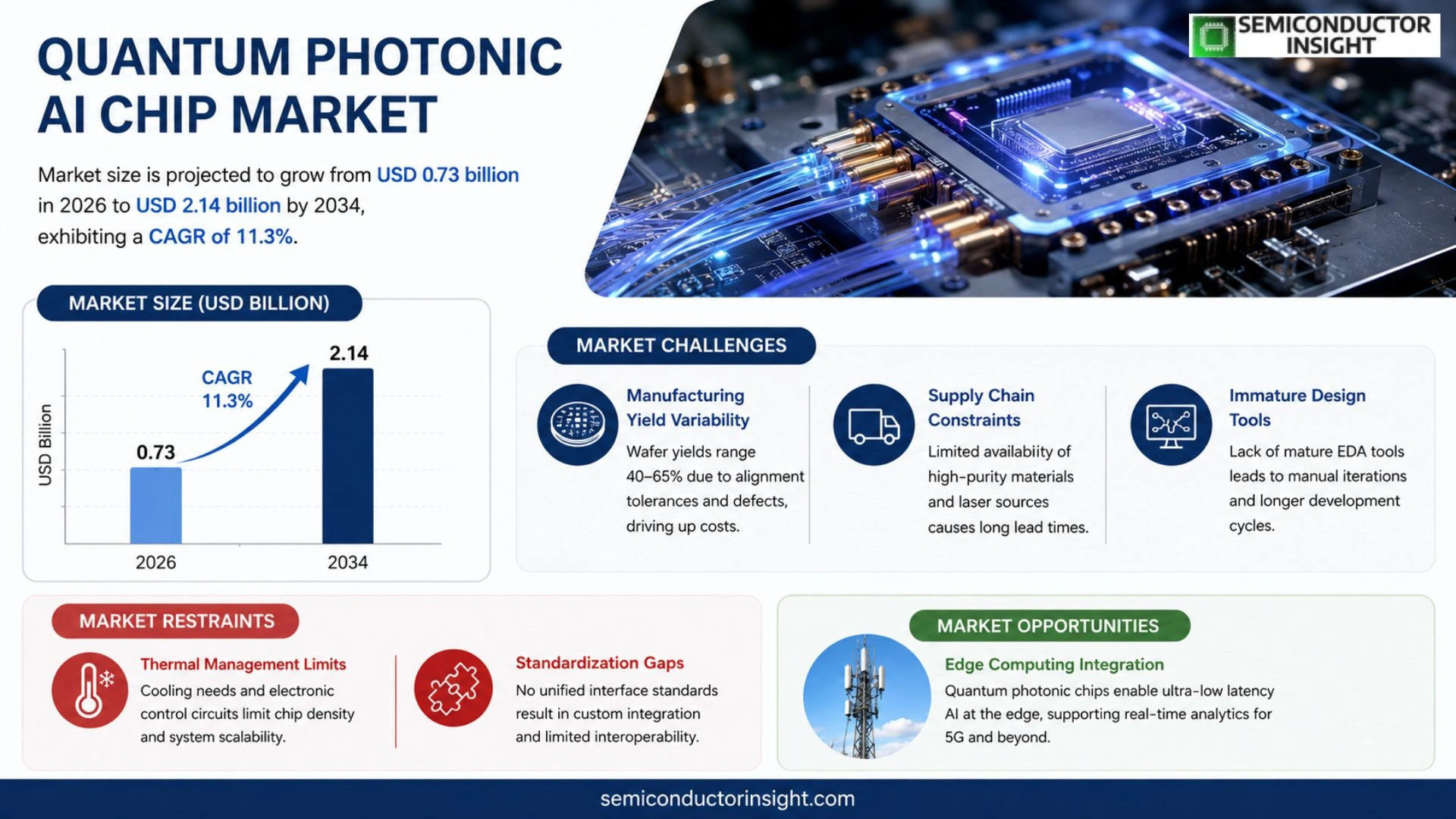
Global Quantum Photonic AI Chip Market size was valued at USD 0.68 billion in 2025. The market is projected to grow from USD 0.73 billion in 2026 to USD 2.14 billion by 2034, exhibiting a CAGR of 11.3 % during the forecast period.
These chips integrate photon‑based interconnects with artificial‑intelligence accelerators, delivering ultra‑low‑latency inference and energy‑efficient training for next‑generation computing workloads. By exploiting entangled photons and on‑chip waveguides, they achieve bandwidths far beyond conventional electronic accelerators while remaining compatible with existing silicon‑photonic platforms.
The sector is gaining momentum because venture capital inflows into quantum hardware have surged, while enterprises look for scalable AI solutions that cut power consumption dramatically. Additionally, collaborations between leading photonics foundries and AI chip designers accelerate product rollouts, positioning the industry for sustained expansion.
MARKET DRIVERS
Advances in Integrated Photonics
The convergence of low‑loss waveguides, on‑chip lasers and high‑speed modulators has lowered the barrier to mass‑produce quantum‑enhanced photonic processors. Companies that can translate laboratory‑scale demonstrations into wafer‑level manufacturing are positioning themselves to capture early‑stage demand from hyperscale AI clusters.
Escalating AI Workload Complexity
Generative models now exceed hundreds of billions of parameters, creating compute profiles that strain conventional electronic GPUs. The intrinsic parallelism of photonic qubits offers a pathway to resolve these bottlenecks, prompting data‑center operators to allocate budget toward experimental photonic AI accelerators.
➤ “When photon‑based inference reaches sub‑microsecond latency, the economics of real‑time AI services shift dramatically.”
Investors are tracking patents that combine quantum error‑correction techniques with silicon‑photonic platforms, because such hybrid designs promise to sustain performance gains even as Moore’s Law decelerates. Strategic funding rounds in the past 12 months reflect a market belief that photonic AI chips will become a cornerstone of next‑generation compute.
MARKET CHALLENGES
Manufacturing Yield Variability
Current photonic foundries report wafer yields ranging from 40 % to 65 % for complex quantum circuits, largely due to alignment tolerances and defect‑induced loss. This variability inflates unit costs and makes pricing models volatile for OEMs seeking volume commitments.
Other Challenges
Supply Chain Constraints
The scarcity of high‑purity silicon‑nitride and specialty laser sources has created a bottleneck that limits the speed at which new fab lines can be qualified. End‑users often experience lead times exceeding six months, which hampers rapid deployment schedules.
In addition, the nascent ecosystem of design‑automation tools for quantum photonic circuits lacks the maturity of electronic EDA suites, forcing engineers to rely on manual layout iterations that extend time‑to‑market.
MARKET RESTRAINTS
Thermal Management Limits
Although photons generate minimal heat during transmission, the accompanying electronic control circuitry and cryogenic cooling required for certain quantum states introduce significant thermal budgets. Integrators must balance chip density with cooling infrastructure, a trade‑off that curtails the scale of deployable systems.
Standardization Gaps
The absence of industry‑wide interface specifications for quantum photonic I/O leads to bespoke integration efforts for each customer. Without a common language, interoperability between vendors remains limited, slowing broader ecosystem adoption.
MARKET OPPORTUNITIES
Edge Computing Integration
Edge nodes that process video streams or sensor data locally can benefit from the ultra‑low latency of photonic inference engines. As 5G rollout accelerates, telecom operators are exploring quantum photonic AI chips to deliver real‑time analytics at the network edge, opening a revenue stream beyond traditional data‑center sales.
Strategic Partnerships and Licensing
Companies that own core photonic IP are forming licensing agreements with semiconductor giants, allowing them to embed quantum photonic cores into existing silicon‑based processors. These collaborations reduce development risk for adopters and create a conduit for rapid market penetration.
Quantum Photonic AI Chip Market Trends
Integration of Photonic Interconnects with AI Acceleration
Combining photon‑based routing with AI‑specific compute blocks is reshaping how data‑intensive workloads are handled. Optical waveguides carry information at terahertz frequencies while preserving signal integrity, allowing inference engines to respond within sub‑nanosecond windows. This speed advantage translates into lower power draw because fewer electronic conversions are required. As enterprises adopt models that exceed the memory bandwidth of conventional silicon, the ability to keep data on‑chip optically becomes a decisive criterion when selecting next‑generation silicon solutions. The shift is not merely technical; it signals a strategic pivot toward architectures that can sustain exponential model growth without proportionally inflating energy costs. Enterprises that prioritize latency‑critical services, such as AI‑driven fraud detection or high‑frequency trading, are already evaluating photonic‑enhanced chips as a viable alternative to traditional GPUs. The reduction in heat dissipation also eases cooling infrastructure demands, allowing data‑center operators to increase rack density without proportionally expanding power‑cabling. Consequently, procurement teams are weighing total‑cost‑of‑ownership metrics that factor in both capital outlay and ongoing energy expenditure, a shift that elevates photonic solutions from experimental prototypes to competitive offerings.
Other Trends
Capital Inflows and Foundry Partnerships
Venture funding directed at quantum‑enabled hardware has risen sharply, prompting photonic foundries to allocate dedicated production lines for AI‑compatible wafers. These collaborations shorten design cycles, as chip architects can leverage mature silicon‑photonic processes while embedding entanglement‑based modules that boost computational density. The financial backing also reduces the risk premium for start‑ups that previously struggled to secure long‑term manufacturing capacity, fostering a more vibrant ecosystem of niche players and larger incumbents alike. Moreover, the alignment of venture capital cycles with government research grants creates a feedback loop that accelerates talent migration toward photonic design houses. Universities that once focused solely on quantum optics now sponsor joint labs with industry, shortening the learning curve for engineers transitioning to mixed‑signal photonic‑electronic platforms. This talent pipeline, combined with shared fab capacity, reduces time‑to‑market for new chip families, compelling incumbents to reassess roadmap timelines.
Emerging Application Segments
Beyond data‑center acceleration, Quantum Photonic AI Chip Market is finding traction in edge devices that demand ultra‑low latency, such as autonomous sensing units and real‑time video analytics. The energy efficiency of photonic links aligns with the power envelopes of remote installations, while the high‑throughput fabric supports complex inference pipelines that were previously confined to centralized servers. Companies that integrate these chips into their product lines can differentiate on response time and operational cost, positioning themselves ahead of competitors still reliant on purely electronic accelerators. Looking ahead, regulatory pressure to curb data‑center carbon footprints is prompting early adopters to quantify the emissions reductions achievable through photonic acceleration. Early case studies indicate a 30 % drop in power usage effectiveness when replacing conventional AI accelerators with optical‑based counterparts. As sustainability metrics become purchasing criteria, vendors that embed photonic modules within their AI stacks are likely to secure preferential contracts with cloud providers committed to green computing initiatives.
COMPETITIVE LANDSCAPE
Key Industry Players
Quantum Photonic AI Chip Market – Competitive Overview
The market is currently anchored by a handful of firms that have marshaled both photonic foundry capacity and AI‑accelerator design expertise. Intel’s silicon‑photonic platform, reinforced by its recent acquisition of a startup specializing in entangled‑photon sources, gives it a clear first‑to‑market advantage in integrating AI inference engines with low‑latency optical interconnects. IBM follows a parallel path, leveraging its quantum‑hardware roadmap to embed photon‑based routing into its AI chip prototypes, thereby offering customers a hybrid compute fabric that bridges quantum‑ready and classical workloads. These two giants shape the overall value chain, dictating standardization choices and influencing the pricing dynamics for upstream component suppliers.
Beyond the dominant players, a cluster of niche innovators is expanding the competitive set. Xanadu and PsiQuantum focus exclusively on scalable photonic qubit arrays, yet both have announced roadmaps that converge on AI‑centric accelerators, positioning them as specialist alternatives for high‑throughput inference. Lightmatter and Luminous Computing differentiate themselves by coupling machine‑learning algorithms with custom waveguide architectures that slash power draw for edge deployments. Smaller ventures such as QuEra Computing, Rigetti, and Cambridge Quantum Computing contribute proprietary entanglement‑generation modules, while D‑Wave and A*STAR provide foundry‑level services that lower entry barriers for emerging designers. The diversity of approaches—from pure‑play photonic startups to established silicon giants—creates a competitive mosaic where collaboration and licensing agreements are as decisive as outright product launches.
List of Key Quantum Photonic AI Chip Companies Profiled
- Intel
- IBM
- Xanadu
- PsiQuantum
- Lightmatter
- Luminous Computing
- QuEra Computing
- Rigetti
- Cambridge Quantum Computing
- D‑Wave Systems
- A*STAR Photonics
- Google Quantum AI
Segment Analysis:
| Segment Category | Sub-Segments | Key Insights |
| By Type |
|
Integrated Photonic AI Chips
|
| By Application |
|
Data Center Acceleration
|
| By End User |
|
Cloud Service Providers
|
| By Technology Architecture |
|
Waveguide‑Based Architecture
|
| By Ecosystem Partner |
|
Photonic Foundries
|
Regional Analysis: Quantum Photonic AI Chip Market
North America
Universities such as MIT, Caltech, and the University of Toronto host interdisciplinary labs that merge quantum optics with silicon photonics, generating a steady stream of peer‑reviewed breakthroughs that feed directly into commercial roadmaps.
Federal programs like the U.S. National Quantum Initiative and Canada’s Quantum Technologies Supercluster allocate multi‑year grants, while strategic corporate venture arms back high‑risk, high‑reward designs that could redefine AI inference.
Early deployments in hyperscale data centers focus on optical interconnects that offload matrix multiplications, demonstrating measurable energy savings and latency reductions compared with traditional electronic accelerators.
Graduate programs in photonic engineering, bolstered by industry‑sponsored internships, ensure a continuous flow of engineers familiar with both quantum theory and chip‑scale fabrication.
Europe
European nations leverage coordinated policy frameworks, such as the European Quantum Flagship, to align national research agendas around photonic AI hardware. Countries like Germany and the Netherlands specialize in low‑loss waveguide platforms, while the UK focuses on algorithm‑hardware co‑design. Industry clusters in the Paris‑Lyon corridor and the Nordic region benefit from strong public‑private partnerships, driving the translation of academic prototypes into niche applications for financial modeling and secure communication. The regulatory environment promotes standards that facilitate cross‑border supply chains, encouraging multinational OEMs to source components from multiple EU facilities.
Asia‑Pacific
Asia‑Pacific offers a contrasting mix of massive manufacturing capacity and emerging quantum research hubs. China’s national labs are rapidly scaling photonic foundries, while Japan’s legacy in silicon photonics supplies mature process nodes to regional start‑ups. South Korea and Singapore invest heavily in AI‑centric chip design curricula, generating talent that bridges software and hardware. Market dynamics are shaped by strong demand from telecom operators seeking integrated photonic transceivers, which in turn accelerates the adoption of AI‑optimized photonic chips for edge‑computing workloads.
South America
South America’s involvement is currently anchored in academic collaborations with North American and European institutions. Brazil’s federal research agencies fund pilot projects that explore low‑cost polymer waveguides, aiming to create a cost‑effective entry point for AI acceleration in agricultural analytics. While production scale remains limited, regional policy incentives for high‑technology exports encourage joint ventures that could position the continent as a niche supplier of customized photonic solutions for renewable‑energy monitoring.
Middle East & Africa
In the Middle East & Africa, investment is concentrated in sovereign wealth‑fund backed technology incubators. The United Arab Emirates has launched a quantum research center that pairs local universities with global chip manufacturers, focusing on secure AI inference for financial services. African markets, led by South Africa’s innovation hubs, are exploring photonic AI chips for satellite‑based imaging, where reduced power consumption aligns with limited on‑board energy budgets. Although the ecosystem is nascent, the strategic emphasis on secure, energy‑efficient computation suggests a gradual rise in relevance for Quantum Photonic AI Chip market.
Report Scope
This market research report provides a comprehensive analysis of the Quantum Photonic AI Chip Market , covering the forecast period 2026–2034. It offers detailed insights into market dynamics, technological advancements, competitive landscape, and key trends shaping the industry.
Key focus areas of the report include:
- Market Overview: The report begins with an overview outlining its current market scenario, key growth indicators, and industry transformation drivers. It discusses macroeconomic factors, demand–supply balance, regulatory landscape, and the strategic role of semiconductors in powering advancements across industries such as automotive, telecommunications, consumer electronics, and industrial automation.
- Market Size & Forecast: Historical data and future projections for revenue, unit shipments, and market value across major regions and segments.
- Segmentation Analysis: Detailed breakdown by product type, technology, application, and end-user industry to identify high-growth segments and investment opportunities.
- Regional Insights: Insights into market performance across North America, Europe, Asia-Pacific, Latin America, and the Middle East & Africa, including country-level analysis where relevant.
- Competitive Landscape: Profiles of leading market participants, including their product offerings, R&D focus, manufacturing capacity, pricing strategies, and recent developments such as mergers, acquisitions, and partnerships.
- Technology Trends & Innovation: Assessment of emerging technologies, integration of AI/IoT, semiconductor design trends, fabrication techniques, and evolving industry standards.
- Market Drivers & Restraints: Evaluation of factors driving market growth along with challenges, supply chain constraints, regulatory issues, and market-entry barriers.
- Stakeholder Insights: Insights for component suppliers, OEMs, system integrators, investors, and policymakers regarding the evolving ecosystem and strategic opportunities.
Primary and secondary research methods are employed, including interviews with industry experts, data from verified sources, and real-time market intelligence to ensure the accuracy and reliability of the insights presented.
FREQUENTLY ASKED QUESTIONS:
What is the current market size of Quantum Photonic AI Chip Market?
-> Quantum Photonic AI Chip Market is projected to grow from USD 0.73 billion in 2026 to USD 2.14 billion by 2034, exhibiting a CAGR of 11.3 %
Which key companies operate in Quantum Photonic AI Chip Market?
-> Key players include leading quantum‑photonic and AI chip firms such as IBM, Google, Intel, Microsoft, PsiQuantum, Lightmatter, and other emerging photonics specialists.
What are the key growth drivers?
-> Key growth drivers include demand for ultra‑low‑latency AI inference, energy‑efficient training, advances in silicon‑photonic integration, and rising venture‑capital investment in quantum hardware.
Which region dominates the market?
-> Region insights were not detailed in the provided source; however, the market is expected to expand globally with strong activity in North America and Asia‑Pacific.
What are the emerging trends?
-> Emerging trends include integration of entangled photon sources, on‑chip waveguide scaling, AI‑optimized photonic architectures, and collaborations between photonics foundries and AI chip designers.

Get Sample Report PDF for Exclusive Insights
Report Sample Includes
- Table of Contents
- List of Tables & Figures
- Charts, Research Methodology, and more...
 Download Sample Report PDF