Precision Semiconductor Lithography Equipment Market Overview
The most important step in semiconductor device fabrication is the lithography where a circuit pattern is transferred from a mask to a wafer or panel by precision Semiconductor Lithography Equipment commonly referred to as steppers or scanners.
This report provides a deep insight into the global Precision Semiconductor Lithography Equipment market covering all its essential aspects. This ranges from a macro overview of the market to micro details of the market size, competitive landscape, development trend, niche market, key market drivers and challenges, SWOT analysis, value chain analysis, etc.
The analysis helps the reader to shape the competition within the industries and strategies for the competitive environment to enhance the potential profit. Furthermore, it provides a simple framework for evaluating and accessing the position of the business organization. The report structure also focuses on the competitive landscape of the Global Precision Semiconductor Lithography Equipment Market, this report introduces in detail the market share, market performance, product situation, operation situation, etc. of the main players, which helps the readers in the industry to identify the main competitors and deeply understand the competition pattern of the market.
In a word, this report is a must-read for industry players, investors, researchers, consultants, business strategists, and all those who have any kind of stake or are planning to foray into the Precision Semiconductor Lithography Equipment market in any manner.
Precision Semiconductor Lithography Equipment Market Analysis:
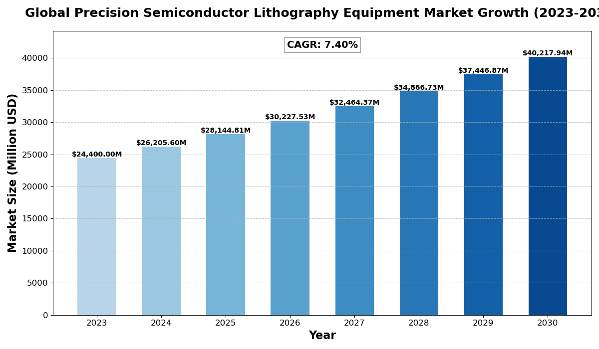
The global Precision Semiconductor Lithography Equipment Market size was estimated at USD 24400 million in 2023 and is projected to reach USD 40217.94 million by 2030, exhibiting a CAGR of 7.40% during the forecast period.
North America Precision Semiconductor Lithography Equipment market size was USD 6357.94 million in 2023, at a CAGR of 6.34% during the forecast period of 2025 through 2030.
Precision Semiconductor Lithography Equipment Key Market Trends :
- Shift Towards Extreme Ultraviolet Lithography (EUV): The adoption of EUV lithography is accelerating due to its ability to enable advanced chip manufacturing at smaller nodes.
- Growing Demand for Advanced Packaging: The need for smaller, high-performance devices is driving demand for precision lithography in advanced packaging applications.
- Expansion of AI and IoT Applications: The rise of AI and IoT technologies is increasing the need for high-performance semiconductor chips, boosting the lithography market.
- Increase in Semiconductor Foundries: Leading foundries are investing in new fabs to meet the rising demand for advanced semiconductor chips.
- Government Support for Semiconductor Manufacturing: Governments worldwide are investing heavily in semiconductor production to strengthen supply chains and technological independence.
Precision Semiconductor Lithography Equipment Market Regional Analysis :

North America:
Strong demand driven by EVs, 5G infrastructure, and renewable energy, with the U.S. leading the market.
Europe:
Growth fueled by automotive electrification, renewable energy, and strong regulatory support, with Germany as a key player.
Asia-Pacific:
Dominates the market due to large-scale manufacturing in China and Japan, with growing demand from EVs, 5G, and semiconductors.
South America:
Emerging market, driven by renewable energy and EV adoption, with Brazil leading growth.
Middle East & Africa:
Gradual growth, mainly due to investments in renewable energy and EV infrastructure, with Saudi Arabia and UAE as key contributors.
Precision Semiconductor Lithography Equipment Market Segmentation :
The research report includes specific segments by region (country), manufacturers, Type, and Application. Market segmentation creates subsets of a market based on product type, end-user or application, Geographic, and other factors. By understanding the market segments, the decision-maker can leverage this targeting in the product, sales, and marketing strategies. Market segments can power your product development cycles by informing how you create product offerings for different segments.
Key Company
- Canon
- Nikon
- ASML Holding NV
- Veeco Instruments Inc.?
- SÜSS MicroTec SE
- JEOL
- Ltd.
- Vistec Semiconductor Systems
Market Segmentation (by Type)
- Deep Ultraviolet Lithography (DUV)
- Extreme Ultraviolet Lithography (EUV)
Market Segmentation (by Application)
- Advanced Packaging
- MEMS Devices
- LED Devices
Drivers
- Rising Demand for High-Performance Computing: The surge in AI, 5G, and IoT applications is fueling the need for high-performance semiconductor devices.
- Technological Advancements in Lithography: Continuous innovations, such as EUV and deep ultraviolet (DUV) lithography, are improving precision and efficiency.
- Expansion of Consumer Electronics Market: Increasing smartphone, laptop, and wearable device production is driving the demand for advanced semiconductor chips.
Restraints
- High Initial Investment and Maintenance Costs: The significant capital required for setting up and maintaining lithography equipment poses a challenge for new entrants.
- Complex Manufacturing Process: The high precision and complexity of semiconductor lithography make it susceptible to production delays and defects.
- Supply Chain Disruptions: Global semiconductor supply chain issues can hinder the timely availability of essential components.
Opportunities
- Growth in Automotive Semiconductors: The rise of electric and autonomous vehicles is increasing demand for high-performance semiconductor chips.
- Expansion in Emerging Markets: Countries like India and Southeast Asia are investing in semiconductor manufacturing, creating new growth avenues.
- Integration of AI in Lithography Equipment: AI-driven process optimization can enhance accuracy and production efficiency in semiconductor lithography.
Challenges
- Regulatory and Trade Restrictions: Geopolitical tensions and export controls can impact the supply chain and global market expansion.
- Shortage of Skilled Workforce: The semiconductor industry faces a shortage of highly skilled professionals for lithography and related processes.
- Environmental Concerns: Stringent regulations regarding waste management and emissions from semiconductor manufacturing can affect production.
Key Benefits of This Market Research:
- Industry drivers, restraints, and opportunities covered in the study
- Neutral perspective on the market performance
- Recent industry trends and developments
- Competitive landscape & strategies of key players
- Potential & niche segments and regions exhibiting promising growth covered
- Historical, current, and projected market size, in terms of value
- In-depth analysis of the Precision Semiconductor Lithography Equipment Market
- Overview of the regional outlook of the Precision Semiconductor Lithography Equipment Market:
Key Reasons to Buy this Report:
- Access to date statistics compiled by our researchers. These provide you with historical and forecast data, which is analyzed to tell you why your market is set to change
- This enables you to anticipate market changes to remain ahead of your competitors
- You will be able to copy data from the Excel spreadsheet straight into your marketing plans, business presentations, or other strategic documents
- The concise analysis, clear graph, and table format will enable you to pinpoint the information you require quickly
- Provision of market value (USD Billion) data for each segment and sub-segment
- Indicates the region and segment that is expected to witness the fastest growth as well as to dominate the market
- Includes in-depth analysis of the market from various perspectives through Porters five forces analysis
- Provides insight into the market through Value Chain
- Market dynamics scenario, along with growth opportunities of the market in the years to come
- 6-month post-sales analyst support
Customization of the Report
In case of any queries or customization requirements, please connect with our sales team, who will ensure that your requirements are met.
FAQs
Q: What are the key driving factors and opportunities in the Precision Semiconductor Lithography Equipment market?
A: The primary drivers include increasing demand for high-performance chips, advancements in EUV and DUV lithography, and growth in AI and IoT applications. Opportunities exist in automotive semiconductors, AI-driven lithography, and emerging markets.
Q: Which region is projected to have the largest market share?
A: The Asia-Pacific region, led by China, Japan, and South Korea, is expected to dominate the market due to strong semiconductor manufacturing capabilities and government investments.
Q: Who are the top players in the global Precision Semiconductor Lithography Equipment market?
A: Leading companies include Canon, Nikon, ASML Holding NV, Veeco Instruments Inc., SÜSS MicroTec SE, JEOL Ltd., and Vistec Semiconductor Systems.
Q: What are the latest technological advancements in the industry?
A: Key advancements include Extreme Ultraviolet (EUV) Lithography, AI-driven process optimization, and high-precision DUV technology, enabling better performance and cost efficiency.
Q: What is the current size of the global Precision Semiconductor Lithography Equipment market?
A: The market size was USD 24,400 million in 2023 and is projected to reach USD 40,217.94 million by 2030, growing at a CAGR of 7.40%.

Get Sample Report PDF for Exclusive Insights
Report Sample Includes
- Table of Contents
- List of Tables & Figures
- Charts, Research Methodology, and more...