Plasma Process Monitor for Semiconductor Market Insights
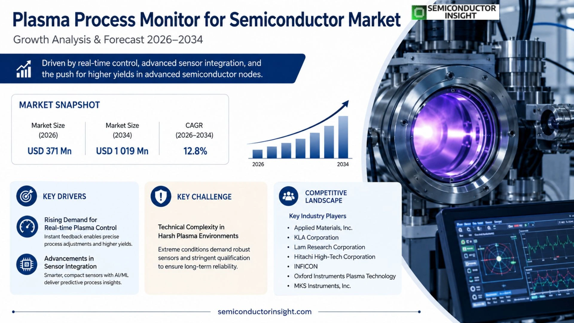
Plasma Process Monitor for Semiconductor market was valued at USD 443 million in 2025 and is forecasted to reach USD 1 019 million by 2034, reflecting a CAGR of 12.8% over the forecast period.
Plasma process monitors are online diagnostic systems installed in etch, clean, CVD, PECVD, PVD, ALD and related steps. They continuously sense plasma‑related variables,optical emission spectra, interferometry signals, RF harmonics, voltage/current statesand exhaust‑gas composition,without interrupting processing, converting these data into real‑time inputsfor process control, equipment maintenanceand yield management. Primary users include equipment OEMs, wafer fabsand IDM manufacturers seeking higher stabilityand reduced downtime. Their ability to detect endpoints, monitor chamber healthand identify abnormal arcs helps shorten recipe development cyclesand lower scrap rates.
MARKET DRIVERS
Rising Demand for Real‑time Plasma Control
Semiconductor fabs are tightening process windows to keep pace with sub‑10 nm node requirements. Plasma Process Monitor for Semiconductor Market solutions that deliver instantaneous feedback enable engineers to adjust power, pressure, and gas mix on the fly, directly influencing critical dimension uniformity. The ability to intervene before a drift becomes permanent translates into measurable yield improvements and a lower cost of ownership for high‑volume manufacturers.
Advancements in Sensor Integration
Recent sensor miniaturisation coupled with edge‑computing platforms allows plasma monitors to be embedded within reactor chambers without compromising throughput. By leveraging machine‑learning models trained on historic process data, these devices now offer predictive alerts rather than simple alarms. This shift from reactive to proactive process control is reshaping equipment procurement strategies across leading foundries.
➤ “Precision monitoring reduces scrap rates and improves yield, making the monitor a strategic asset rather than an optional add‑on.”
The convergence of tighter design tolerances, smarter diagnostics, and the growing economic incentive to maximise wafer output creates a compelling case for investment. Companies that adopt integrated plasma monitoring early are positioning themselves to capture incremental revenue from reduced cycle times and superior product quality.
MARKET CHALLENGES
Technical Complexity in Harsh Plasma Environments
Plasma reactors expose instrumentation to extreme temperatures, high‑energy ions, and corrosive chemistries. Designing sensors that remain calibrated over extended runs demands specialised materials and rigorous qualification procedures. Failure to address these reliability constraints can erode the perceived value of the monitor and increase maintenance overhead.
Other Challenges
Calibration Frequency
Frequent recalibration cycles are often required to maintain accuracy, leading to scheduled downtime that conflicts with tight fab production windows. Balancing the need for precision against operational continuity remains a delicate engineering problem for many adopters.
MARKET RESTRAINTS
High Capital Expenditure for Cutting‑edge Instruments
The upfront cost of deploying state‑of‑the‑art plasma monitoring systems exceeds the budget thresholds of many mid‑size fabs. While the long‑term return on investment is attractive, the initial outlay,often bundled with software licences and integration services,creates a financial barrier that slows adoption, especially in regions where fab expansion is still emerging.
MARKET OPPORTUNITIES
Emerging Applications in Advanced Packaging
Advanced packaging techniques such as fan‑out wafer‑level packaging and 3D‑IC stacking rely on plasma‑based etch and deposition steps that are highly sensitive to process variance. Incorporating real‑time plasma monitoring into these workflows offers a pathway to tighter electrical performance tolerances and higher throughput, opening a new revenue stream for monitor vendors seeking to diversify beyond traditional wafer‑fabrication segments.
Plasma Process Monitor for Semiconductor Market Trends
Integration of Sensor Platforms into Tool Architecture
The latest wave of equipment design is embedding plasma monitoring capability directly into process modules rather than treating it as an after‑thought add‑on. Vendors such as Hamamatsu and INFICON now ship clamp‑on heads, embedded software stacks, and FDC/APC interfaces as standard options on new etch and deposition tools. This shift reduces installation time, eliminates the need for separate calibration rigs, and creates a unified data pipeline that feeds real‑time control algorithms. For fab managers, the practical effect is a tighter correlation between sensor read‑outs and recipe adjustments, which translates into fewer wafer re‑runs and a measurable drop in overall equipment effectiveness (OEE) losses. The move also reshapes the revenue model: hardware sales are complemented by recurring licensing fees for analytics packages, positioning suppliers to capture longer‑term value from a single instrumentation footprint.
Other Trends
Shift Toward Algorithm‑Driven Diagnostics
Beyond raw signal capture, the market is investing heavily in machine‑learning models that translate optical emission spectra, RF harmonics, and gas‑analysis data into actionable fault predictions. Companies such as Plasmetrex and Prime Solution have introduced libraries that flag micro‑arcing events and anticipate chamber drift before yield impact becomes observable. This predictive layer is especially valuable in high‑aspect‑ratio etch where a single out‑of‑spec cycle can cost thousands of dollars in scrap. Customers that adopt these algorithms report a reduction of test wafer usage by up to 30 % and faster ramp‑up on new process nodes, giving them a competitive edge in time‑to‑market for advanced logic and HBM‑driven memory products.
Regional Concentration of Supply and Demand
Supply expertise remains clustered in Japan, South Korea, Europe, and the United States, each region leveraging distinct technical strengths,optical spectroscopy in Japan, RF diagnostics in Europe, and integrated software ecosystems in the U.S. Meanwhile, demand follows the concentration of 300 mm fabs in East Asia and the growing investment pipeline in the United States fueled by policy incentives such as CHIPS for America. This geographic mismatch is prompting OEMs to co‑develop monitoring modules with local suppliers, ensuring that interface standards and support structures align with regional fab practices. For vendors, securing early design‑win partnerships in emerging clusters,particularly in China, Taiwan, and Korea,offers a pathway to scale platform‑level solutions beyond niche endpoint detectors.
COMPETITIVE LANDSCAPE
Key Industry Players
Competitive Outlook for Plasma Process Monitors in Semiconductor Fabrication
The market is anchored by a handful of technology powerhouses that have turned optical emission spectroscopy and interferometry into mature, production‑grade platforms. Hamamatsu Photonics leverages its legacy in photon detection to supply high‑speed sensor heads that integrate seamlessly with etch and CVD tools, while HORIBA builds on a similar optical foundation but adds a suite of software algorithms that translate spectral data into actionable process control signals. INFICON and MKS Instruments complement the optical camp with RF‑based sensing and gas‑phase analysis, offering manufacturers a broader diagnostic envelope that includes arc detection and exhaust composition monitoring. These four firms dominate the revenue tier because they combine deep wafer‑fab relationships, extensive service networks, and the ability to bundle hardware with recurring software licences. Their product roadmaps increasingly emphasize embedded modules and cloud‑linked analytics, reinforcing a market structure where value resides as much in data processing as in the sensor itself.
Beyond the headline players, a diverse set of niche innovators is reshaping the competitive dynamics. PLASUS supplies compact clamp‑on sensors that excel in low‑open‑area etch environments, while Extrel’s mass‑spectrometry approach provides unparalleled sensitivity to trace contaminants. Plasmetrex and Prime Solution specialize in molecular‑beam sampling, delivering real‑time gas‑composition read‑outs that feed directly into advanced APC loops. NANOTECH and Impedans focus on electron‑density measurement and collision‑rate diagnostics, targeting high‑aspect‑ratio etch processes where traditional optics struggle. These companies differentiate through specialised form factors, proprietary algorithms, or regional proximity to leading fabs in Japan, Korea and Taiwan. Their agility lets them capture segments of the market that require bespoke integration or rapid deployment, and they often act as preferred suppliers for pilot‑line projects or next‑generation node development.
List of Key Plasma Process Monitor for Semiconductor Companies Profiled
- Hamamatsu Photonics
- HORIBA
- INFICON
- MKS Instruments
- PLASUS
- Extrel
- Plasmetrex GmbH
- Prime Solution Co., Ltd.
- NANOTECH, Inc.
- Impedans Ltd.
- Advanced Plasma Analytics
- Synapse Monitoring Systems
- Quantum Sensor Technologies
- EuroPlasma Diagnostics
- SiliconEdge Instruments
Segment Analysis:
| Segment Category | Sub-Segments | Key Insights |
| By Type |
|
Leading Segment – Optical and interferometric techniques dominate because they provide non‑intrusive, rapid feedback that aligns with high‑throughput etch and deposition tools.
|
| By Application |
|
Leading Segment – Etch and clean applications drive adoption because precise endpoint and arc detection directly protect high‑value pattern fidelity.
|
| By End User |
|
Leading Segment – Foundries prioritize plasma monitors to sustain high‑volume production stability.
|
| By Sensing Principle |
|
Leading Segment – Optical emission remains core because of its speed, but firms are expanding RF and gas‑analysis capabilities to cover low‑open‑area etch and subtle contamination events.
|
| By Installation Position |
|
Leading Segment – Clamp‑on and exhaust‑side installations are gaining traction because they preserve chamber integrity while delivering rich plasma diagnostics.
|
Regional Analysis: Plasma Process Monitor for Semiconductor Market
North America
Vendors are embedding machine‑learning models directly within the plasma monitoring hardware, allowing facilities to anticipate defect formation minutes before it manifests on the wafer. This preemptive capability reduces scrap rates and aligns well with the cost‑sensitivity of high‑mix production lines.
Companies are decoupling sensor arrays from the main monitor chassis, offering plug‑and‑play upgrades. This modularity extends equipment life cycles and lowers total cost of ownership, a critical factor for fabs facing tight investment timelines.
As environmental regulations tighten, providers are bundling compliance documentation with their monitoring suites, simplifying audit trails and ensuring that plasma emissions stay within permissible limits.
By processing data at the equipment edge, latency drops dramatically, enabling closed‑loop control that reacts within sub‑second intervals,crucial for maintaining uniformity across 300‑mm wafers.
Europe
European fabs are leveraging the continent’s strong standards framework to standardise plasma monitoring protocols across multiple sites. The collaborative approach between equipment manufacturers and research consortia is driving a wave of interoperable solutions that can be redeployed across different process nodes. Companies are also focusing on sustainability, integrating energy‑efficiency metrics into the monitoring software, which resonates with the EU’s carbon‑reduction agenda. As a result, European buyers are favouring platforms that balance performance with regulatory compliance, creating a niche market for high‑precision, low‑footprint monitors.
Asia‑Pacific
In the Asia‑Pacific, the surge in advanced node adoption is compelling foundries to refine plasma control to achieve tighter tolerances. Local governments are investing heavily in semiconductor parks, and this influx of capital is prompting OEMs to introduce cost‑effective monitoring kits tailored for volume production. Additionally, the region’s supply‑chain density enables rapid iteration cycles, allowing manufacturers to test emerging sensor technologies in pilot lines before scaling globally. The competitive pressure is spurring a race to embed diagnostics that can operate across a broader range of plasma chemistries.
South America
South America’s semiconductor footprint, though modest, is expanding through strategic partnerships with North American and European players. The region’s emerging fabs are adopting plasma process monitors primarily to offset the experience gap, relying on turnkey solutions that bundle installation, training, and remote support. This approach accelerates knowledge transfer and reduces the learning curve associated with high‑mix, low‑volume production, positioning the market for incremental growth as local demand for advanced electronics rises.
Middle East & Africa
The Middle East & Africa are at an early stage of semiconductor manufacturing, yet ambitious national initiatives are laying the groundwork for future fabs. Early adopters are focusing on scalable monitoring platforms that can be integrated into multi‑purpose pilot lines, providing a flexible foundation for later expansion. Partnerships with global OEMs are emphasising knowledge sharing, ensuring that the region can quickly adopt best‑in‑class plasma diagnostics once larger projects come online. This preparatory phase is critical for establishing a competent supply chain capable of supporting Plasma Process Monitor for Semiconductor Market in the years ahead.
Report Scope
This market research report provides a comprehensive analysis of the Plasma Process Monitor for Semiconductor Market , covering the forecast period 2026–2034. It offers detailed insights into market dynamics, technological advancements, competitive landscape, and key trends shaping the industry.
Key focus areas of the report include:
- Market Overview: The report begins with an overview outlining its current market scenario, key growth indicators, and industry transformation drivers. It discusses macroeconomic factors, demand–supply balance, regulatory landscape, and the strategic role of semiconductors in powering advancements across industries such as automotive, telecommunications, consumer electronics, and industrial automation.
- Market Size & Forecast: Historical data and future projections for revenue, unit shipments, and market value across major regions and segments.
- Segmentation Analysis: Detailed breakdown by product type, technology, application, and end-user industry to identify high-growth segments and investment opportunities.
- Regional Insights: Insights into market performance across North America, Europe, Asia-Pacific, Latin America, and the Middle East & Africa, including country-level analysis where relevant.
- Competitive Landscape: Profiles of leading market participants, including their product offerings, R&D focus, manufacturing capacity, pricing strategies, and recent developments such as mergers, acquisitions, and partnerships.
- Technology Trends & Innovation: Assessment of emerging technologies, integration of AI/IoT, semiconductor design trends, fabrication techniques, and evolving industry standards.
- Market Drivers & Restraints: Evaluation of factors driving market growth along with challenges, supply chain constraints, regulatory issues, and market-entry barriers.
- Stakeholder Insights: Insights for component suppliers, OEMs, system integrators, investors, and policymakers regarding the evolving ecosystem and strategic opportunities.
Primary and secondary research methods are employed, including interviews with industry experts, data from verified sources, and real-time market intelligence to ensure the accuracy and reliability of the insights presented.
FREQUENTLY ASKED QUESTIONS:
What is the current market size of Plasma Process Monitor for Semiconductor Market?
-> Plasma Process Monitor for Semiconductor market is forecasted to reach USD 1 019 million by 2034, reflecting a CAGR of 12.8% over the forecast period.
Which key companies operate in Plasma Process Monitor for Semiconductor Market?
-> Key players include Hamamatsu Photonics, HORIBA, PLASUS, Extrel, Plasmetrex GmbH, INFICON, MKS Inc., Impedans Ltd., NANOTECH, Inc., and Prime Solution Co., Ltd.
What are the key growth drivers?
-> Key growth drivers include expansion of advanced logic and high‑bandwidth memory (HBM) driven fabs, increasing number of advanced deposition and etch steps, tighter process windows at advanced nodes, and heightened demand for reduced downtime and higher yield.
Which region dominates the market?
-> Asia (particularly East Asia – China, Japan, South Korea, and Taiwan) leads demand, while the United States follows as a major secondary market.
What are the emerging trends?
-> Emerging trends include integration of sensor heads into cluster tools, software‑driven algorithm platforms for real‑time process control, AI‑enabled drift prediction, and the shift from standalone endpoint detectors to comprehensive process‑sensing platforms.

Get Sample Report PDF for Exclusive Insights
Report Sample Includes
- Table of Contents
- List of Tables & Figures
- Charts, Research Methodology, and more...