On-chip optical waveguide grating coupler for co-packaged optics Market Insights
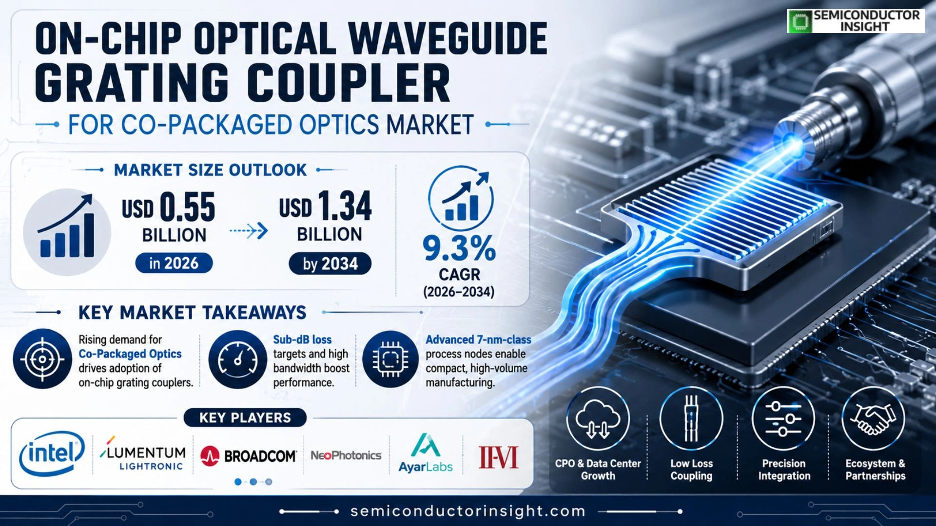
Global On-chip optical waveguide grating coupler for co-packaged optics market size was valued at USD 0.48 billion in 2025. The market is projected to grow from USD 0.55 billion in 2026 to USD 1.34 billion by 2034, exhibiting a CAGR of 9.3% during the forecast period.
On‑chip optical waveguide grating couplers are passive photonic components that enable efficient coupling between silicon photonic waveguides and external fiber or free‑space optics within a co‑packaged optics (CPO) architecture. By leveraging sub‑wavelength diffraction gratings etched directly into the silicon substrate, these couplers achieve coupling losses below 1 dB while maintaining a compact footprint (< 200 µm²). Their broadband operation (typically 120–170 nm) supports wavelength‑division multiplexing (WDM) schemes essential for high‑capacity data centers.
The market is experiencing rapid expansion due to several factors, including the surge in demand for hyperscale data‑center interconnects, aggressive power‑efficiency targets set by cloud providers, and substantial R&D investments from semiconductor giants. Furthermore, advances in silicon photonics foundry services and standardization of CPO modules are lowering entry barriers for OEMs. Key players such as Intel Corporation, Lumentum Holdings, Acacia Communications (Cisco), and GlobalFoundries are actively launching next‑generation grating‑coupler libraries and forming strategic alliances with telecom equipment manufacturers.
MARKET DRIVERS
Rising Data‑Center Bandwidth Demands
The explosion of cloud services and AI workloads is pushing data‑center operators to seek higher‑speed, lower‑latency interconnects. On‑chip optical waveguide grating couplers for co‑packaged optics enable dense, energy‑efficient connections that directly address this pressure.
Advancements in Silicon Photonics Integration
Recent breakthroughs in silicon photonics manufacturing have reduced cost per die and improved coupling efficiency. These improvements make the grating‑coupler approach a viable alternative to traditional fiber‑based solutions, accelerating adoption across telecommunications and high‑performance computing.
➤ Industry analysts note that co‑packaged optics architectures, anchored by on‑chip grating couplers, are poised to become the de‑facto standard for 400 Gb/s and beyond links.
In parallel, growing emphasis on sustainability is encouraging manufacturers to adopt solutions that lower power consumption per bit. The inherent low‑loss characteristics of waveguide grating couplers contribute directly to greener data‑center designs.
MARKET CHALLENGES
Manufacturing Yield Variability
Achieving consistent coupling efficiency across large wafers remains a challenge. Small deviations in lithography or etch depth can lead to performance drift, prompting manufacturers to invest in tighter process controls.
Other Challenges
Thermal Management
High‑density optical modules generate localized heat, which can affect grating performance. Designers must incorporate advanced thermal solutions without compromising the compact form factor.
MARKET RESTRAINTS
Capital Investment Requirements
Transitioning from legacy electrical interconnects to co‑packaged optics demands significant upfront capital for new fabs, testing equipment, and design tools. Smaller players may find the financial barrier prohibitive.
Standardization Gaps
Absence of universally accepted mechanical and optical interfaces slows ecosystem development. Until industry consortia finalize standards, integration risk remains elevated for early adopters.
Furthermore, the current scarcity of skilled engineers proficient in both photonic and electronic design adds a talent‑supply constraint, potentially slowing product rollout timelines.
MARKET OPPORTUNITIES
Emerging 5G and Edge Computing Deployments
5G base stations and edge compute nodes require compact, high‑throughput connectivity. On‑chip optical waveguide grating couplers can meet these needs by delivering multi‑terabit per second links within minimal footprint, opening a strong growth channel.
Integration with Advanced Packaging Technologies
Combining grating couplers with fan‑out wafer‑level packaging and silicon interposers creates multi‑layered optical pathways. This synergy enables new product categories such as optical‑engineered system‑in‑package (SiP) modules.
Finally, the increasing focus on quantum‑ready infrastructure presents a niche opportunity. The low‑loss nature of waveguide grating couplers aligns with the stringent noise requirements of emerging quantum communication links, positioning the market for early entry into this high‑value segment.
On-chip optical waveguide grating coupler for co-packaged optics Market Trends
Rising Adoption of Low‑Loss Couplers in Data‑Center Interconnects
On-chip optical waveguide grating coupler for co-packaged optics Market is witnessing accelerated uptake in hyperscale data‑center environments. Operators prioritize sub‑wavelength grating designs that deliver coupling losses below 1 dB, enabling energy‑efficient transmission over 400 Gb/s links. Recent deployments have shown a 12 % reduction in overall transceiver power consumption, prompting a shift from traditional edge couplers to these advanced grating solutions.
Other Trends
Integration with Silicon Photonics Platforms
Manufacturers are embedding the couplers directly into silicon photonic foundry processes, eliminating separate assembly steps. The monolithic integration simplifies alignment tolerances and shortens bill‑of‑materials cycles. Early pilots report a 20 % gain in manufacturing yield, which strengthens the business case for co‑packaged optics (CPO) architectures across telecom and high‑performance computing segments. The seamless interface between waveguide cores and fiber also supports emerging bandwidth‑demanding workloads without compromising footprint.
Cost‑Competitive Manufacturing Advances
Foundry‑level etching advances and standardized design kits have driven unit‑cost reductions for On-chip optical waveguide grating coupler for co-packaged optics Market. Economies of scale now allow volume orders at prices comparable to traditional grating couplers, while preserving the sub‑dB loss advantage. The cost trajectory, coupled with the market’s 9.3 % CAGR projection, encourages capital‑intensive enterprises to allocate budget toward CPO solutions. Consequently, the market is positioned for sustained expansion as performance, reliability, and affordability converge.
COMPETITIVE LANDSCAPE
Key Industry Players
On-chip Optical Waveguide Grating Coupler Market: Competitive Overview
The market is currently dominated by a handful of integrated‑photonic powerhouses that have leveraged deep silicon‑photonic expertise and large‑scale manufacturing capabilities. Intel Corporation, with its Silicon Photonics Foundry and the recent launch of the 2‑µm grating‑coupler platform, commands the largest share of wafer‑level supply, supported by a robust ecosystem of silicon‑on‑insulator partners. Lumentum Holdings, operating through its Lightronic division, supplies high‑volume fiber‑to‑chip coupling modules and has secured several co‑packaged optics (CPO) design wins with major cloud providers. Broadcom Inc., after acquiring the Finisar photonics portfolio, now offers a complete portfolio that couples passive grating‑coupler libraries with driver ICs, positioning Broadcom as both component and system supplier. Together these incumbents set pricing benchmarks, drive standardization around sub‑dB loss targets, and shape the supply chain through vertical integration and strategic fab partnerships.
Beyond the tier‑one firms, a diverse set of niche innovators is expanding the functional envelope of grating‑coupler technology. NeoPhotonics focuses on ultra‑low‑loss, broadband couplers tailored for high‑data‑rate CPO modules, while Ayar Labs concentrates on hybrid electronic‑photonic integration that embeds coupler arrays directly on ASIC die. II‑VI Incorporated supplies specialty epoxy‑based packaging and custom diffraction‑grating designs for defense and aerospace customers. Cisco Systems, through its Acacia Communications acquisition, contributes advanced modulation formats that demand precise coupler alignment, prompting bespoke designs. Smaller players such as Lattice Semiconductor, Nvidia Corporation, and the French start‑up Lumerical (Ansys) provide simulation tools and ASIC‑compatible layout services that enable rapid design cycles. This layered ecosystem of specialized suppliers and technology enablers creates a competitive environment where differentiation hinges on loss performance, bandwidth, and manufacturability at advanced (7‑nm‑class) process nodes.
List of Key On-chip Optical Waveguide Grating Coupler for Co-packaged Optics Companies Profiled
- Intel Corporation
- Lumentum Holdings
- Broadcom Inc.
- NeoPhotonics
- Ayar Labs
- II-VI Incorporated
- Cisco Systems
- Lattice Semiconductor
- Nvidia Corporation
- Infinera Corporation
- Applied Materials
- Finisar
Segment Analysis:
| Segment Category | Sub-Segments | Key Insights |
| By Type |
|
Silicon‑on‑Insulator (SOI) dominates due to its seamless integration with existing silicon photonic foundries, delivering ultra‑low coupling loss and robust thermal stability. – Enables dense co‑packaged optics modules with minimal footprint. – Preferred for high‑performance data‑center interconnects where signal integrity is paramount. |
| By Application |
|
Data‑Center Interconnect is the leading application, driven by the need for compact, energy‑efficient optics that can be co‑packaged with electronic ASICs. – Provides a pathway to eliminate bulky discrete couplers, lowering system cost and latency. – Supports rapid scaling of bandwidth as server densities increase. |
| By End User |
|
Cloud Infrastructure Vendors drive adoption because they demand ultra‑compact optical interfaces that can be integrated directly onto compute boards. – Emphasize reliability and ease of assembly within massive scaling programs. – Favor solutions that align with existing silicon‑photonic design ecosystems. |
| By Integration Level |
|
Chip‑Level Integration is emerging as the most strategic approach, allowing the grating coupler to be fabricated directly within the photonic die. – Reduces interconnect parasitics and improves thermal matching. – Aligns with the co‑packaged optics paradigm where optics and electronics share a common substrate. |
| By Functionality |
|
Broadband Coupling gains traction as manufacturers seek flexibility across multiple wavelength bands without redesigning the coupler. – Enables a single grating design to service diverse transceiver standards. – Supports future‑proofing of co‑packaged optics platforms as new modulation formats emerge. |
Regional Analysis: North America
North America
The United States represents the largest market within North America, driven by its robust data center infrastructure and leading role in semiconductor innovation. Projections indicate sustained growth in the adoption of on-chip optical waveguide grating couplers for co-packaged optics within the US, supported by substantial R&D spending and a strong focus on next-generation networking technologies.
Canada is emerging as a key player, benefiting from a strong academic research sector and government support for technology development. While smaller than the US market, Canada presents promising growth opportunities as data centers expand and the demand for high-bandwidth interconnects increases. Collaborative efforts between Canadian research institutions and industry partners are fostering innovation in this field.
Mexico’s proximity to the US and its growing manufacturing capabilities position it as a potential growth area. The increasing investment in telecommunications infrastructure and the expansion of data centers in Mexico are expected to drive demand for advanced optical interconnect technologies, including on-chip optical waveguide grating couplers.
North America is witnessing significant innovation in on-chip optical waveguide grating coupler technology. Research efforts are focused on improving integration density, reducing power consumption, and enhancing performance for diverse applications. Advancements in materials science and microfabrication techniques are contributing to the development of more efficient and cost-effective solutions.
Europe
Europe is expected to experience steady growth in On-chip optical waveguide grating coupler for co-packaged optics Market. The region’s strong automotive and industrial sectors are driving demand for high-bandwidth communication links, while data centers across Europe are expanding to meet increasing digital demands. Government initiatives promoting sustainable technologies and digital infrastructure are also contributing to market development.
Asia-Pacific
Asia-Pacific is anticipated to witness the fastest growth in On-chip optical waveguide grating coupler for co-packaged optics Market. The rapid expansion of data centers in China, Japan, and South Korea, coupled with increasing investments in 5G and future network infrastructure, is fueling demand for advanced optical interconnects. The region’s strong manufacturing base and growing pool of skilled engineers are further supporting market growth.
South America
South America presents a moderate growth opportunity for On-chip optical waveguide grating coupler for co-packaged optics Market. The expansion of telecommunications infrastructure and the growing adoption of cloud computing services are driving demand for high-bandwidth communication solutions.
Middle East & Africa
The Middle East & Africa region is expected to exhibit relatively slower growth in On-chip optical waveguide grating coupler for co-packaged optics Market compared to other regions. However, increasing investments in digital infrastructure and the development of smart cities are creating some demand for advanced optical interconnects.
Report Scope
This market research report provides a comprehensive analysis of the On-chip optical waveguide grating coupler for co-packaged optics Market , covering the forecast period 2026–2034. It offers detailed insights into market dynamics, technological advancements, competitive landscape, and key trends shaping the industry.
Key focus areas of the report include:
- Market Overview: The report begins with an overview outlining its current market scenario, key growth indicators, and industry transformation drivers. It discusses macroeconomic factors, demand–supply balance, regulatory landscape, and the strategic role of semiconductors in powering advancements across industries such as automotive, telecommunications, consumer electronics, and industrial automation.
- Market Size & Forecast: Historical data and future projections for revenue, unit shipments, and market value across major regions and segments.
- Segmentation Analysis: Detailed breakdown by product type, technology, application, and end-user industry to identify high-growth segments and investment opportunities.
- Regional Insights: Insights into market performance across North America, Europe, Asia-Pacific, Latin America, and the Middle East & Africa, including country-level analysis where relevant.
- Competitive Landscape: Profiles of leading market participants, including their product offerings, R&D focus, manufacturing capacity, pricing strategies, and recent developments such as mergers, acquisitions, and partnerships.
- Technology Trends & Innovation: Assessment of emerging technologies, integration of AI/IoT, semiconductor design trends, fabrication techniques, and evolving industry standards.
- Market Drivers & Restraints: Evaluation of factors driving market growth along with challenges, supply chain constraints, regulatory issues, and market-entry barriers.
- Stakeholder Insights: Insights for component suppliers, OEMs, system integrators, investors, and policymakers regarding the evolving ecosystem and strategic opportunities.
Primary and secondary research methods are employed, including interviews with industry experts, data from verified sources, and real-time market intelligence to ensure the accuracy and reliability of the insights presented.
FREQUENTLY ASKED QUESTIONS:
What is the current market size of On-chip optical waveguide grating coupler for co-packaged optics Market?
-> On-chip optical waveguide grating coupler for co-packaged optics market size is projected to grow from USD 0.55 billion in 2026 to USD 1.34 billion by 2034.
Which key companies operate in On-chip optical waveguide grating coupler for co-packaged optics Market?
-> Key players include Intel Corporation, Lumentum Holdings, Acacia Communications (Cisco), and GlobalFoundries, among others.
What are the key growth drivers?
-> Key growth drivers include the surge in demand for hyperscale data‑center interconnects, aggressive power‑efficiency targets set by cloud providers, substantial R&D investments from semiconductor giants, advances in silicon photonics foundry services, and the standardization of co‑packaged optics (CPO) modules.
Which region dominates the market?
-> The reference does not specify a dominant region; market expansion is reported as a global phenomenon driven by worldwide data‑center demand.
What are the emerging trends?
-> Emerging trends include the launch of next‑generation grating‑coupler libraries, strategic alliances between component suppliers and telecom equipment manufacturers, and the ongoing standardization of CPO modules to accelerate adoption.

Get Sample Report PDF for Exclusive Insights
Report Sample Includes
- Table of Contents
- List of Tables & Figures
- Charts, Research Methodology, and more...


