MARKET INSIGHTS
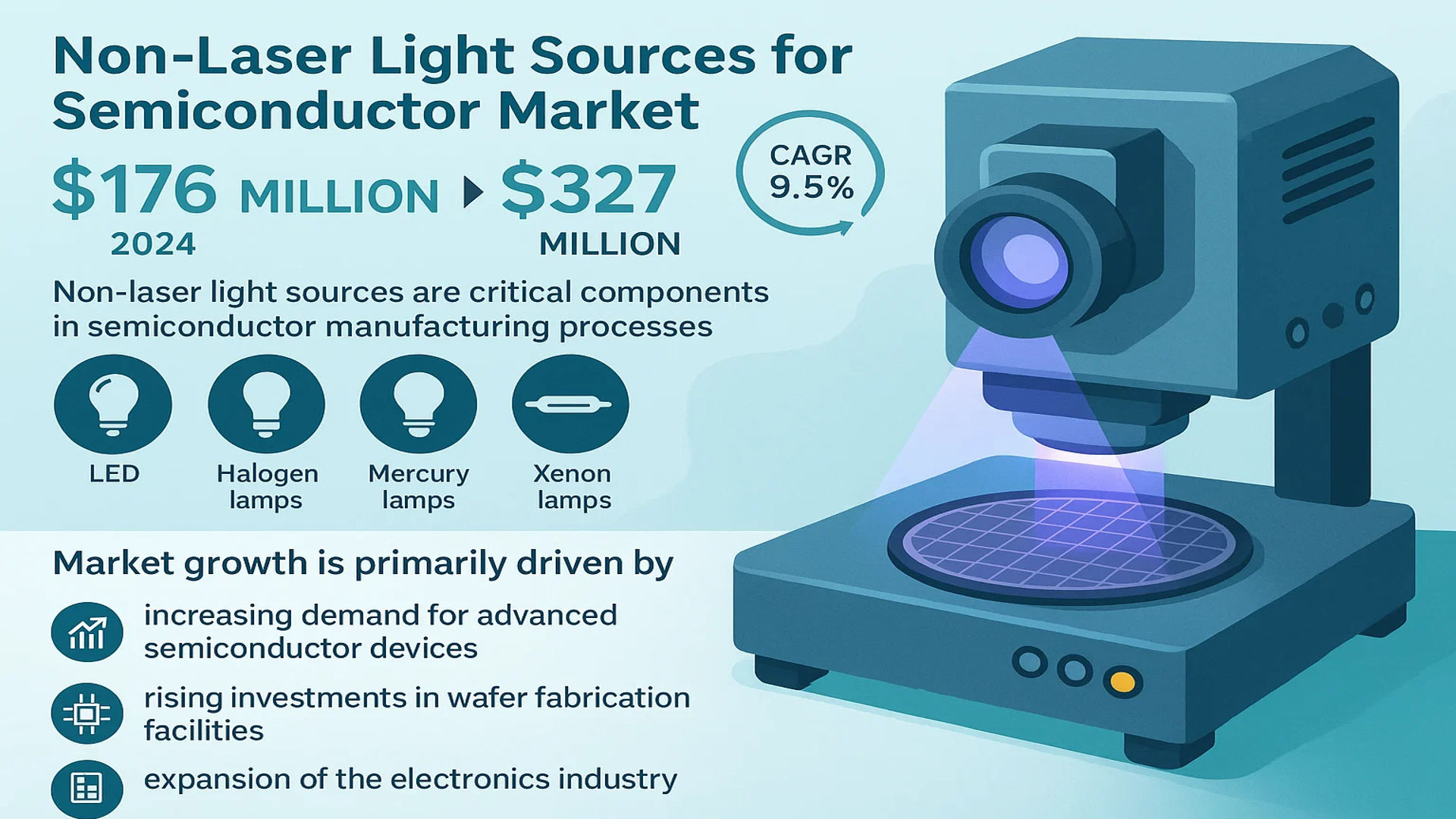
The global Non-Laser Light Sources for Semiconductor Market was valued at 176 million in 2024 and is projected to reach US$ 327 million by 2032, at a CAGR of 9.5% during the forecast period.
Non-laser light sources are critical components in semiconductor manufacturing processes, providing precise and uniform illumination for applications such as photolithography, inspection, metrology, and annealing. These light sources, which include LED, halogen lamps, mercury lamps, and xenon lamps, are preferred in applications where laser-based systems are either unnecessary or impractical due to cost or technical constraints.
Market growth is primarily driven by increasing demand for advanced semiconductor devices, rising investments in wafer fabrication facilities, and the expansion of the electronics industry. The LED light source segment is expected to grow significantly due to its energy efficiency and longer lifespan compared to traditional lamps. Furthermore, key players like USHIO, Signify NV, and Hamamatsu Photonics are continuously innovating to enhance light source performance, which is expected to further propel market expansion.
MARKET DYNAMICS
MARKET DRIVERS
Advancements in Semiconductor Manufacturing Processes Fuel Demand for Non-Laser Light Sources
The semiconductor industry is experiencing unprecedented growth with wafer production volumes projected to exceed 15 million units annually by 2026. This expansion directly increases the demand for reliable non-laser light sources in critical processes like photolithography and inspection. Traditional halogen and mercury lamp technologies have evolved significantly, offering improved spectral stability and longer operational lifetimes exceeding 4,000 hours in most industrial applications. The ability to provide uniform illumination across large semiconductor wafers makes these non-coherent light sources indispensable for high-precision manufacturing operations. Additionally, recent breakthroughs in LED technology have enabled some systems to achieve optical power densities comparable to traditional lamps while reducing energy consumption by approximately 40%.
Growing Adoption of Advanced Packaging Technologies Drives Market Expansion
Advanced packaging techniques such as 3D IC stacking and fan-out wafer-level packaging are becoming increasingly prevalent, with the market for these technologies expected to grow at a compound annual growth rate of over 14% through 2030. These packaging methods require precise alignment and inspection processes that extensively utilize non-laser illumination systems. Xenon-based light sources have demonstrated particular effectiveness in these applications due to their broad spectral output and high intensity. Furthermore, the transition to smaller node sizes below 7nm has created new demands for inspection systems capable of detecting nanometer-scale defects, where controlled illumination becomes critical. Market leaders have responded by developing specialized light source configurations with tunable wavelengths to address these emerging requirements.
Cost-Effectiveness of Non-Laser Systems Compared to Laser Alternatives Supports Market Penetration
While laser-based systems offer superior coherence, non-laser light sources provide significant economic advantages with acquisition costs typically 25-35% lower than comparable laser solutions. This cost differential becomes particularly important for high-volume manufacturing where systems are deployed in parallel. Moreover, the total cost of ownership is further reduced through simpler maintenance requirements and the ability to replace individual components rather than entire systems. In inspection applications, modern LED-based systems have achieved detection capabilities approaching those of lasers for many defect types, making them increasingly attractive for quality control operations. The ability to precisely control illumination angles and intensities in these systems has closed much of the performance gap while maintaining economic benefits.
MARKET RESTRAINTS
Limitations in Precision Compared to Laser Systems Constrains Critical Applications
Despite significant advancements, non-laser light sources still face fundamental limitations in applications requiring extremely high spatial coherence. In photolithography processes for nodes below 5nm, the lack of perfect collimation in conventional illumination systems can create challenges in pattern fidelity. This has led some manufacturers to continue preferring laser-based systems for these cutting-edge applications, particularly in EUV lithography implementations. Additionally, thermal management remains a challenge for high-intensity operations, where lamp degradation can affect spectral output stability. While advanced cooling systems have mitigated these issues substantially, they still require careful monitoring and maintenance to ensure consistent performance over extended operational periods.
Regulatory Pressure on Mercury-Based Systems Impacts Market Segments
Environmental regulations affecting mercury-containing light sources have created uncertainty in this segment of the market. Some regions have implemented strict controls on mercury content in industrial equipment, prompting manufacturers to accelerate development of alternative technologies. While LED alternatives continue to improve, certain specialized applications still rely on the unique spectral characteristics of mercury vapor lamps. The transition has been challenging for inspection systems that depend on precise wavelength emissions at 365nm, 405nm, and 436nm spectral lines. Compliance costs associated with these regulatory changes have added approximately 12-16% to the development budgets of affected products, creating short-term pressures on profitability.
Other Restraints
Supply Chain Disruptions
The semiconductor equipment sector has experienced significant supply chain challenges affecting critical components for light source manufacturing. Lead times for certain optical elements and power supplies have extended to 12-16 weeks in some cases, creating bottlenecks in system production. These disruptions have been particularly acute for xenon lamp components where specialized materials are required.
Technology Transition Periods
The shift from traditional lamps to solid-state alternatives requires substantial retooling and retraining investments. Many fabrication facilities operate on tight schedules that make equipment transitions challenging, slowing adoption of next-generation systems despite their long-term benefits.
MARKET OPPORTUNITIES
Emerging Applications in Heterogeneous Integration Create New Growth Avenues
The rapid development of heterogeneous integration technologies presents significant opportunities for non-laser light source providers. As semiconductor manufacturers increasingly combine different chip technologies into single packages, the need for specialized inspection and alignment systems grows accordingly. This trend is particularly evident in the development of chiplets, where precise optical alignment becomes critical. Market leaders are investing in customized illumination solutions that can address the unique requirements of these multi-die systems. Recent product launches have demonstrated the ability to provide tailored spectral outputs optimized for distinguishing different materials and structures in complex 3D assemblies.
Expansion of Compound Semiconductor Manufacturing Opens New Markets
The growing adoption of compound semiconductors for power electronics and RF applications is creating demand for specialized process equipment, including inspection and metrology systems. Gallium nitride and silicon carbide wafer processing present unique challenges that conventional silicon-focused systems are not always optimized to address. This has spurred development of new illumination configurations specifically designed for these materials, with several major equipment providers introducing products targeting this niche. The compound semiconductor market is projected to maintain double-digit growth rates through the decade, providing a sustained expansion opportunity for specialized light source technologies.
Integration of AI-Based Inspection Creates Demand for Advanced Illumination Controls
The implementation of machine learning algorithms in semiconductor inspection systems is driving requirements for more sophisticated illumination capabilities. AI-enhanced systems benefit from multi-angle and multi-spectral imaging that requires precise light source control. This has led to development of smart illumination systems with programmable intensity profiles and spectral tuning capabilities. The ability to dynamically adjust illumination parameters based on defect detection patterns allows for more efficient inspection processes, reducing false positives and improving throughput. Equipment manufacturers are increasingly viewing illumination as an active component of the inspection system rather than just a passive light source.
MARKET CHALLENGES
Intense Competition from Laser-Based Solutions in Precision Applications
Non-laser light sources face persistent competition from advanced laser systems in applications requiring the highest levels of precision. While significant progress has been made in improving the performance characteristics of conventional illumination, laser systems maintain advantages in certain critical parameters. The spot size and coherence length of laser illumination remain superior for applications like mask alignment and certain metrology tasks. Laser manufacturers continue to drive down costs through technological improvements, narrowing the price differential that has traditionally favored non-laser solutions. This competitive pressure requires continuous innovation from non-laser system providers to maintain their value proposition.
Other Challenges
Thermal Management Limitations
High-power illumination systems generate significant thermal loads that can affect performance stability. Managing these thermal effects becomes increasingly challenging as intensity requirements grow for advanced inspection applications. While modern cooling systems have improved significantly, they add complexity and cost to overall system designs.
Spectral Stability Over Operational Lifetime
Maintaining consistent spectral output throughout a light source’s operational life remains a technical challenge, particularly for traditional lamp technologies. The gradual degradation of lamp electrodes and phosphors can lead to subtle shifts in spectral characteristics that may impact measurement consistency. Advanced monitoring and compensation systems have been developed but represent an added cost burden.
NON-LASER LIGHT SOURCES FOR SEMICONDUCTOR MARKET TRENDS
Rise of Advanced Manufacturing Processes Driving Market Expansion
The global non-laser light sources market for semiconductors has witnessed significant growth due to the increasing demand for precise and uniform illumination in semiconductor manufacturing. With photolithography, inspection, and annealing applications requiring high-performance lighting solutions, technologies such as LED, halogen lamps, mercury lamps, and xenon lamps have become critical. The market was valued at $176 million in 2024 and is projected to expand at a CAGR of 9.5%, reaching $327 million by 2032. The growing adoption of LED light sources is particularly notable due to their energy efficiency, longer lifespan, and precise spectral control. Additionally, the U.S. continues to lead in market share, while China is emerging as a key growth region, driven by semiconductor infrastructure investments.
Other Trends
Shift Towards Hybrid Light Source Solutions
Manufacturers are increasingly integrating hybrid light source systems to enhance flexibility and performance in semiconductor fabrication. Combining LED and xenon lamps, for example, provides both energy efficiency and high-intensity illumination required for advanced lithography processes. The segment for LED light sources alone is expected to grow substantially, supported by continuous technological advancements that improve brightness, spectral range, and longevity. Furthermore, decreasing production costs of LEDs have made them more accessible for large-scale semiconductor manufacturing facilities.
Increasing Demand for Semiconductor Inspection and Metrology
The semiconductor industry’s emphasis on yield optimization and defect detection has heightened the need for non-laser light sources in inspection and metrology applications. High-resolution imaging systems rely heavily on precisely calibrated lighting to detect nanometer-scale defects. Companies such as Hamamatsu Photonics and Excelitas Technologies are developing advanced illumination systems optimized for automated optical inspection (AOI) equipment. Additionally, innovations in ultraviolet (UV) and deep-ultraviolet (DUV) light sources are enabling better defect detection in next-generation semiconductor nodes, supporting the market’s growth trajectory.
COMPETITIVE LANDSCAPE
Key Industry Players
Innovation and Strategic Partnerships Drive Market Competition
The global non-laser light sources for semiconductor market is characterized by a competitive yet fragmented landscape, with established players and emerging innovators vying for market share. USHIO Inc. leads the industry due to its comprehensive portfolio of high-performance LED and xenon lamp solutions, which are widely adopted in photolithography and inspection applications. The company’s strong foothold in Asia and North America has positioned it as a key market influencer.
Closely following USHIO, ams OSRAM and Hamamatsu Photonics have carved out significant market shares. These companies are known for their precision light sources used in semiconductor manufacturing, leveraging advanced R&D capabilities to maintain technological leadership. Hamamatsu, in particular, has gained traction with its mercury lamp solutions, which remain critical for legacy semiconductor processes.
Another notable player, Excelitas Technologies, differentiates itself with customized lighting solutions tailored for semiconductor annealing and etching applications. The company’s focus on energy-efficient LED technology aligns with the industry’s shift toward sustainable manufacturing practices.
Meanwhile, Signify NV (formerly Philips Lighting) has been expanding its footprint through strategic acquisitions and collaborations, particularly in the inspection and measurement segment. Their emphasis on smart lighting solutions for semiconductor fabrication plants has resonated with manufacturers seeking to optimize operational efficiency.
List of Key Non-Laser Light Source Companies Profiled
- USHIO Inc. (Japan)
- ams OSRAM (Germany)
- Hamamatsu Photonics (Japan)
- Excelitas Technologies (U.S.)
- Signify NV (Netherlands)
- ARC (U.S.)
- Heraeus (Germany)
- Nikon Corporation (Japan)
- YUMEX (Japan)
- OPT Machine Vision Tech (China)
- Changzhou Yuyu Electro-optical Device (China)
Segment Analysis:
By Type
LED Light Source Segment Leads Due to Energy Efficiency and Long Lifespan
The market is segmented based on type into:
- LED Light Source
- Subtypes: UV LED, Visible LED, and others
- Halogen Lamp
- Mercury Lamp
- Subtypes: High-pressure, Low-pressure, and others
- Xenon Lamp
- Others
By Application
Inspection and Measurement Segment Dominates Due to Rising Semiconductor Quality Standards
The market is segmented based on application into:
- Inspection and measurement
- Photolithography
- Annealing
- Marking and Etching
- Others
Regional Analysis: Non-Laser Light Sources for Semiconductor Market
Asia-Pacific
Asia-Pacific dominates the global non-laser light sources market for semiconductors, with China, Japan, and South Korea leading in production and consumption. The region accounts for over 45% of global semiconductor manufacturing, creating substantial demand for LED, halogen, and xenon lamp technologies. China’s aggressive semiconductor self-sufficiency push, including the US$ 150 billion Made in China 2025 initiative, has accelerated adoption across photolithography and inspection applications. However, Japan remains the technology leader, with companies like Hamamatsu Photonics and USHIO driving innovations in mercury lamp alternatives. While cost-effective LED solutions gain traction, mercury lamps still dominate critical processes due to their wavelength precision.
North America
The North American market prioritizes high-performance non-laser solutions for advanced packaging and 3D NAND applications, with the U.S. accounting for approximately 28% of global R&D investment in semiconductor light technologies. Regulatory pressures are phasing out mercury lamps, creating opportunities for Excelitas Technologies’ UV LED systems in inspection equipment. The CHIPS and Science Act’s US$ 52 billion funding is spurring domestic semiconductor production, indirectly boosting demand for localized light source suppliers. Thermal annealing applications increasingly use customized xenon lamp systems from firms like Heraeus, particularly for AI and HPC chip manufacturing.
Europe
Europe maintains a niche position in specialty light sources, with ams OSRAM and Signify NV leading in deep UV LED development for semiconductor metrology. Strict RoHS and REACH regulations have accelerated the transition from mercury to LED-based systems, particularly in Germany’s automotive semiconductor sector. However, the market growth is restrained by limited local semiconductor fabrication capacity, with most demand coming from equipment manufacturers supplying Asian foundries. Collaborative projects like the EU Chips Act aim to rebuild local production capabilities, which could revive demand for advanced non-laser illumination systems in photolithography by 2030.
South America
South America represents an emerging market, primarily serving back-end semiconductor processes with imported light source systems. Brazil shows growing demand for LED-based inspection tools in its consumer electronics assembly sector, though economic instability limits capital investment. Argentina’s nascent semiconductor packaging industry utilizes refurbished halogen lamp systems for cost-sensitive applications. The lack of local manufacturers creates opportunities for Asian suppliers, but adoption of advanced technologies remains 5-7 years behind leading markets due to infrastructure limitations.
Middle East & Africa
This region focuses on downstream semiconductor applications, with Israel and UAE importing specialized xenon lamp systems for military and aerospace component manufacturing. Saudi Arabia’s US$ 100 billion investment in NEOM’s technology hub may create future demand for wafer inspection equipment. However, the absence of local semiconductor fabrication results in minimal direct consumption, with most light source applications confined to university research labs and electronics repair facilities using basic halogen systems. Partnerships with Chinese suppliers are gradually introducing LED alternatives for industrial marking applications.
Report Scope
This market research report provides a comprehensive analysis of the Global Non-Laser Light Sources for Semiconductor Market, covering the forecast period 2024–2032. It offers detailed insights into market dynamics, technological advancements, competitive landscape, and key trends shaping the industry.
Key focus areas of the report include:
- Market Size & Forecast: Historical data and future projections for revenue, unit shipments, and market value across major regions and segments. The market was valued at USD 176 million in 2024 and is projected to reach USD 327 million by 2032, growing at a CAGR of 9.5%.
- Segmentation Analysis: Detailed breakdown by product type (LED Light Source, Halogen Lamp, Mercury Lamp, Xenon Lamp) and application (Inspection and Measurement, Photolithography, Annealing, Marking and Etching, Others) to identify high-growth segments.
- Regional Outlook: Insights into market performance across North America, Europe, Asia-Pacific, Latin America, and the Middle East & Africa. The U.S. and China are key markets with significant growth potential.
- Competitive Landscape: Profiles of leading market participants including USHIO, Signify NV, ams OSRAM, Excelitas Technologies, and Hamamatsu Photonics, covering their product portfolios, R&D investments, and strategic initiatives.
- Technology Trends & Innovation: Assessment of emerging light source technologies, integration with semiconductor manufacturing processes, and evolving industry standards.
- Market Drivers & Restraints: Evaluation of factors driving market growth (semiconductor industry expansion, advanced packaging demand) along with challenges (high equipment costs, regulatory constraints).
- Stakeholder Analysis: Strategic insights for semiconductor manufacturers, equipment suppliers, and investors regarding market opportunities and competitive positioning.
The report employs rigorous primary and secondary research methodologies, including interviews with industry experts and analysis of verified market data, to ensure accuracy and reliability.
FREQUENTLY ASKED QUESTIONS:
What is the current market size of Global Non-Laser Light Sources for Semiconductor Market?
-> Non-Laser Light Sources for Semiconductor Market was valued at 176 million in 2024 and is projected to reach US$ 327 million by 2032, at a CAGR of 9.5% during the forecast period.
Which key companies operate in this market?
-> Key players include USHIO, Signify NV, ams OSRAM, Excelitas Technologies, Hamamatsu Photonics, and Nikon, among others.
What are the key growth drivers?
-> Growth is driven by increasing semiconductor production, demand for advanced packaging, and the expansion of IoT and AI applications requiring precise light-based processes.
Which region dominates the market?
-> Asia-Pacific leads the market due to semiconductor manufacturing concentration, while North America shows strong growth in R&D applications.
What are the emerging trends?
-> Emerging trends include high-efficiency LED adoption, miniaturization of light sources, and integration with smart manufacturing systems.

Get Sample Report PDF for Exclusive Insights
Report Sample Includes
- Table of Contents
- List of Tables & Figures
- Charts, Research Methodology, and more...

