MARKET INSIGHTS
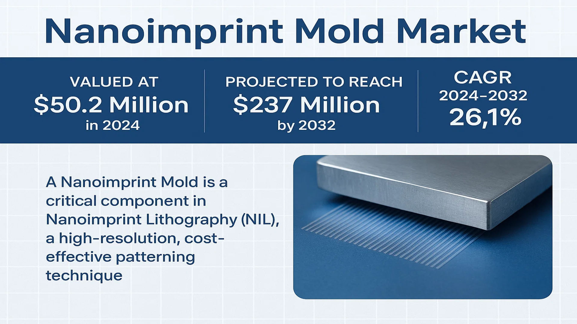
The global Nanoimprint Mold Market was valued at 50.2 million in 2024 and is projected to reach US$ 237 million by 2032, at a CAGR of 26.1% during the forecast period.
A Nanoimprint Mold is a critical component in Nanoimprint Lithography (NIL), a high-resolution, cost-effective patterning technique. These molds are master templates, typically fabricated from durable materials like silicon or quartz, that are used to physically imprint nanoscale features directly onto a substrate. This process enables the fabrication of intricate structures with resolutions below 10 nanometers, surpassing the limitations of traditional optical lithography and offering significant cost reductions, estimated at 30-50% compared to conventional methods.
The market is experiencing explosive growth primarily driven by its technological advantages and expanding downstream applications. As Moore’s Law approaches its physical limits, the exorbitant cost of extreme ultraviolet (EUV) lithography systems, which can exceed USD 150 million per unit, has made nanoimprinting a compelling alternative for advanced semiconductor manufacturing. A key recent development underscoring this trend is the collaboration between Kioxia and Canon to implement NIL technology for the mass production of 3D NAND flash memory, which is a major factor fueling demand for high-precision molds. Furthermore, growth is bolstered by diverse applications beyond semiconductors, including micro-optics for augmented reality devices and biological sensors. Leading players such as NTT Advanced Technology, DNP, and NIL Technology operate in this market with specialized portfolios.
MARKET DYNAMICS
MARKET DRIVERS
Advancements in Semiconductor Manufacturing to Drive Nanoimprint Mold Demand
The semiconductor industry’s relentless pursuit of miniaturization and cost efficiency is significantly driving the nanoimprint mold market. As traditional photolithography approaches its physical and economic limits—with extreme ultraviolet (EUV) lithography systems costing over $150 million per unit—nanoimprint lithography (NIL) emerges as a viable alternative offering sub-10 nm resolution at 30-50% lower manufacturing costs. This technological advantage has prompted major semiconductor manufacturers to adopt NIL for advanced memory production. For instance, Kioxia Corporation’s collaboration with Canon to implement NIL technology in 3D NAND flash memory production has created substantial demand for high-precision nanoimprint molds. The global semiconductor industry’s projected growth to over $600 billion by 2025 further underscores the potential for nanoimprint mold adoption across various semiconductor applications.
Expanding Applications in Optical Devices and Photonics to Boost Market Growth
The expanding applications of nanoimprint technology in optical devices and photonics represent another significant market driver. Nanoimprint molds enable the cost-effective production of sophisticated optical components including diffraction gratings, microlens arrays, and photonic crystals with feature sizes below 100 nm. The global photonics market, valued at approximately $750 billion, increasingly relies on NIL for manufacturing advanced optical elements used in augmented reality displays, optical sensors, and telecommunications equipment. The ability to create complex nanostructures with high reproducibility makes nanoimprint molds particularly valuable for producing anti-reflective coatings, light-guiding plates, and other optical elements that require precise nanoscale patterning. This diversification beyond semiconductor applications provides additional growth avenues for the nanoimprint mold market.
Growing Investment in Research and Development to Accelerate Market Expansion
Substantial investments in research and development activities are accelerating innovation and adoption of nanoimprint technology across multiple industries. Both public and private sectors are increasing funding for nanotechnology research, with global nanotechnology funding exceeding $30 billion annually. Academic institutions, research organizations, and corporations are actively developing new applications for nanoimprint lithography in areas such as biomedical devices, energy storage systems, and advanced materials. The development of novel mold materials with enhanced durability and improved release properties has addressed previous limitations, making NIL more commercially viable. These ongoing R&D efforts are not only improving nanoimprint mold performance but also reducing production costs, thereby expanding the addressable market for this technology.
MARKET CHALLENGES
High Initial Investment and Manufacturing Complexity to Challenge Market Penetration
The nanoimprint mold market faces significant challenges related to high initial investment requirements and manufacturing complexity. Fabricating high-quality nanoimprint molds demands specialized equipment, cleanroom facilities, and advanced metrology tools, resulting in substantial capital expenditure. The production process involves multiple intricate steps including electron-beam lithography, reactive ion etching, and surface treatment, requiring highly skilled technicians and engineers. This complexity contributes to manufacturing yields that typically range between 60-80% for complex patterns, increasing the effective cost per usable mold. Additionally, the need for regular mold maintenance and potential refurbishment adds ongoing operational expenses, making it challenging for smaller companies to enter the market or for NIL to compete in price-sensitive applications.
Other Challenges
Technical Limitations in Pattern Transfer Fidelity
Maintaining pattern transfer fidelity across numerous imprint cycles presents a persistent technical challenge. Even with advanced mold materials, gradual degradation occurs due to mechanical stress, adhesion issues, and contamination accumulation. This degradation can lead to pattern distortion, defective imprints, and reduced mold lifespan. The industry standard currently achieves approximately 10,000-50,000 imprints per mold depending on pattern complexity and material properties, which may be insufficient for high-volume manufacturing requirements. Developing mold materials that can withstand millions of imprint cycles while maintaining nanoscale precision remains an ongoing technical hurdle that affects the economic viability of nanoimprint technology for mass production applications.
Material Compatibility and Defect Management Issues
Material compatibility issues between molds and various resist materials create significant challenges in achieving defect-free patterning. Differences in surface energy, thermal expansion coefficients, and chemical interactions can lead to pattern defects, sticking problems, and incomplete filling. The management of nanoscale defects, particularly for patterns below 20 nm, requires sophisticated inspection systems and cleaning protocols that add complexity and cost to the manufacturing process. These material compatibility challenges become particularly pronounced when working with novel resist materials or when transitioning between different application domains, limiting the flexibility and adoption breadth of nanoimprint technology across diverse industrial sectors.
MARKET RESTRAINTS
Limited Production Throughput and Scalability Issues to Restrain Market Growth
Despite its advantages in resolution and cost, nanoimprint lithography faces significant restraints related to production throughput and scalability challenges. The sequential nature of the imprinting process limits overall production speed compared to parallel processing methods like photolithography. Current nanoimprint systems typically achieve throughput rates of 10-20 wafers per hour for 300 mm substrates, which falls short of the 100+ wafers per hour capability of advanced photolithography tools. This throughput limitation becomes particularly constraining for high-volume semiconductor manufacturing where production efficiency directly impacts profitability. The industry’s transition toward larger substrate sizes further exacerbates these scalability challenges, as maintaining uniform pressure and alignment across larger areas becomes increasingly difficult with current nanoimprint technology.
Intellectual Property Barriers and Standardization Issues to Hinder Market Development
Intellectual property complexities and lack of industry standardization present additional restraints for the nanoimprint mold market. The technology landscape is fragmented with multiple competing approaches and proprietary methodologies, creating interoperability challenges between different nanoimprint systems and molds. This fragmentation discourages potential adopters who fear vendor lock-in or compatibility issues. Furthermore, the dense patent landscape surrounding nanoimprint technology creates legal uncertainties and potential infringement risks for market participants. The absence of universally accepted standards for mold specifications, interface protocols, and quality metrics complicates the development of multi-vendor ecosystems and slows down the technology’s maturation toward mainstream adoption in industrial manufacturing environments.
Competition from Alternative Patterning Technologies to Limit Market Expansion
The nanoimprint mold market faces significant competition from emerging alternative patterning technologies that threaten to limit its expansion potential. Techniques such as directed self-assembly (DSA), multi-beam electron beam lithography, and advanced photolithography extensions continue to evolve, offering improved resolution, throughput, and defect control. The semiconductor industry’s substantial existing investment in conventional lithography infrastructure creates considerable inertia against adopting fundamentally different technologies like NIL. Additionally, the development of EUV lithography with single-digit nanometer resolution capabilities, despite its high cost, provides an alternative path for advanced patterning that may capture market segments that would otherwise consider nanoimprint technology. This competitive pressure necessitates continuous innovation and cost reduction to maintain the value proposition of nanoimprint molds in the broader patterning technology landscape.
MARKET OPPORTUNITIES
Emerging Applications in Biomedical and Life Sciences to Create New Growth Opportunities
The expanding applications of nanoimprint technology in biomedical and life sciences present substantial growth opportunities for the nanoimprint mold market. The ability to create precise nanoscale patterns on various substrates enables the development of advanced biomedical devices, including lab-on-chip systems, biosensors, and tissue engineering scaffolds. The global biomedical diagnostics market, projected to exceed $100 billion, increasingly incorporates nanofabricated components for improved detection sensitivity and specificity. Nanoimprint molds facilitate the cost-effective production of nanofluidic channels, surface-enhanced Raman spectroscopy substrates, and cell culture platforms with controlled surface topographies. These applications leverage the unique capability of NIL to create hierarchical structures spanning multiple length scales, opening new revenue streams beyond traditional electronics and optics applications.
Advancements in Mold Materials and Fabrication Techniques to Enable Market Expansion
Recent advancements in mold materials and fabrication techniques are creating significant opportunities for market expansion. The development of durable mold materials such as diamond-like carbon coatings, advanced metal alloys, and composite materials has substantially improved mold longevity and performance. These material innovations enable 100,000+ imprint cycles for certain applications, reducing the cost per imprint and making NIL more competitive for high-volume production. Additionally, improvements in fabrication techniques including multi-step patterning, 3D nanostructuring, and hybrid approaches combining different lithography methods allow creation of increasingly complex nanostructures. These technological advancements expand the application range of nanoimprint molds into new domains such as quantum computing devices, advanced energy harvesting systems, and metamaterials with tailored electromagnetic properties.
Growing Adoption in Flexible Electronics and Wearable Devices to Drive Future Demand
The rapid growth of flexible electronics and wearable devices represents a promising opportunity for nanoimprint mold market expansion. Unlike conventional lithography, NIL can pattern directly on flexible substrates including polymers, paper, and textiles, making it ideally suited for emerging applications in flexible displays, electronic skin, and smart textiles. The global flexible electronics market, expected to reach $50 billion, requires cost-effective patterning methods that can accommodate non-planar surfaces and withstand mechanical deformation. Nanoimprint technology’s ability to create functional nanostructures on diverse materials positions it advantageously for these applications. The development of roll-to-roll nanoimprint processes further enhances this opportunity by enabling continuous manufacturing of flexible electronic components, potentially revolutionizing production methods for next-generation wearable devices and Internet of Things sensors.
NANOIMPRINT MOLD MARKET TRENDS
Semiconductor Industry Adoption as a Cost-Effective Alternative to EUV Lithography
The semiconductor industry’s relentless pursuit of miniaturization, driven by Moore’s Law, is a primary catalyst for the nanoimprint mold market. As traditional photolithography techniques like Extreme Ultraviolet (EUV) lithography face significant cost barriers—with a single tool costing upwards of $150 million—nanoimprint lithography (NIL) emerges as a compelling, cost-effective alternative. This trend is particularly pronounced in the memory sector, where the demand for high-density storage is insatiable. A landmark development underscoring this shift is the strategic partnership between Kioxia and Canon to integrate NIL technology into the mass production of 3D NAND flash memory. This collaboration validates NIL’s capability to achieve sub-10 nm resolutions, a critical threshold for next-generation semiconductors, while simultaneously reducing the overall manufacturing cost by an estimated 30% to 50%. This significant cost advantage, coupled with proven high-resolution capabilities, is accelerating the transition from R&D to high-volume manufacturing, thereby creating sustained and growing demand for precision nanoimprint molds.
Other Trends
Expansion into Advanced Optics and Photonics Applications
Beyond semiconductors, the market is experiencing robust growth driven by the expansion into micro and nano optics. NIL is uniquely suited for fabricating complex optical elements like diffraction gratings, microlens arrays, and anti-reflective surfaces with unparalleled precision and at a lower cost than other nanofabrication methods. The global augmented and virtual reality (AR/VR) market, projected to be a multi-billion dollar industry, relies heavily on these miniature optical components for near-eye displays and sensors. Furthermore, the telecommunications sector utilizes NIL molds to produce advanced photonic integrated circuits (PICs) and optical metasurfaces that manipulate light in novel ways. The ability to rapidly prototype and mass-produce these intricate structures is fueling investments from optical device manufacturers, who require durable and highly precise molds to maintain product consistency and performance across large production runs.
Material and Fabrication Technology Innovations
Innovation in mold materials and fabrication techniques constitutes a critical trend shaping the competitive landscape of the market. While silicon and quartz remain industry standards due to their excellent mechanical properties and thermal stability, there is increasing development and adoption of harder, more wear-resistant materials like nickel alloys and diamond-like carbon (DLC) coatings to enhance mold longevity. The lifetime of a mold is a key economic factor, as frequent replacement can erode the cost benefits of NIL. Consequently, advancements in atomic layer deposition (ALD) and other surface treatment technologies are being employed to create ultra-durable, anti-stiction layers that prevent pattern damage during the de-molding process. Simultaneously, progress in electron-beam lithography and focused ion beam (FIB) milling is enabling the creation of molds with even more complex and finer features, pushing the boundaries of what is possible in nanofabrication and opening new application avenues in fields such as biomedical devices and nanofluidics.
COMPETITIVE LANDSCAPE
Key Industry Players
Technological Innovation and Strategic Partnerships Drive Market Positioning
The global nanoimprint mold market exhibits a semi-consolidated structure, characterized by a mix of established multinational corporations and specialized technology firms. This dynamic is fueled by the high technical barriers to entry, including the need for advanced nanofabrication capabilities and significant R&D investment. While no single player dominates the entire market, several companies have carved out strong positions through technological leadership and strategic market expansion.
NTT Advanced Technology Corporation (Japan) is widely recognized as a pioneer and a leading force, particularly due to its early and sustained investment in nanoimprint lithography (NIL) research. The company’s expertise in creating high-precision, durable molds, especially for the optoelectronics and photonics sectors, has secured its significant market share. Similarly, Dai Nippon Printing (DNP) (Japan) leverages its vast experience in precision printing and microfabrication to produce high-quality quartz and silicon molds, making it a key supplier for semiconductor and display applications.
The competitive intensity is further heightened by specialized technology providers. Nanonex (U.S.) not only supplies molds but also develops and sells complete NIL systems, creating a vertically integrated offering that strengthens its customer value proposition. NIL Technology (Denmark) focuses on diffractive optical elements and meta-optics, positioning itself at the forefront of this high-growth application segment. Meanwhile, European players like Eulitha (Switzerland) are noted for their innovative mold fabrication techniques and strong presence in the research and development community.
Asian manufacturers are increasingly influential, competing aggressively on both technology and cost. Companies such as IMS Chips (Germany, with a strong international presence), Temicon (Germany), and Hangzhou Ouguangxin Technology (China) are expanding their production capacities and technological capabilities to capture a larger portion of the global demand. Their growth is largely driven by the booming semiconductor and electronics industries within the Asia-Pacific region, which accounted for the largest market share in 2024.
Looking forward, the competitive landscape is expected to evolve through increased merger and acquisition activity as larger semiconductor equipment companies seek to acquire NIL expertise. Furthermore, continuous innovation in mold materials—to enhance durability and enable higher-resolution patterning—will be a critical differentiator for maintaining a competitive edge in this rapidly advancing market.
List of Key Nanoimprint Mold Companies Profiled
- NTT Advanced Technology Corporation (Japan)
- Dai Nippon Printing Co., Ltd. (DNP) (Japan)
- Tekscend Photomask (Taiwan)
- IMS Chips (Germany)
- Hangzhou Ouguangxin Technology Co., Ltd. (China)
- Temicon GmbH (Germany)
- Yingsheng Electronic Technology Co., Ltd. (China)
- Nanonex Corporation (U.S.)
- Eulitha AG (Switzerland)
- NIL Technology ApS (Denmark)
Segment Analysis:
By Type
Silicon Molds Segment Dominates the Market Due to Superior Mechanical Properties and Cost-Effectiveness
The market is segmented based on type into:
- Silicon Molds
- Quartz Molds
- Metal Molds
- Polymer Molds
- Others
By Application
Semiconductor Segment Leads Due to High Adoption in Advanced Chip Manufacturing and Memory Devices
The market is segmented based on application into:
- Semiconductor
- Micro and Nano Optics
- Biomedical Devices
- Photonic Devices
- Others
By End User
Foundries and IDMs Segment Leads Due to Massive Scale Production Requirements and Technological Investments
The market is segmented based on end user into:
- Foundries and Integrated Device Manufacturers (IDMs)
- Research and Academic Institutions
- Optoelectronics Companies
- Biotechnology and Medical Device Firms
By Technology
UV-Nanoimprint Lithography Segment Leads Due to High Throughput and Compatibility with Various Resins
The market is segmented based on technology into:
- UV-Nanoimprint Lithography (UV-NIL)
- Thermal Nanoimprint Lithography (T-NIL)
- Roll-to-Roll Nanoimprint Lithography (R2R-NIL)
- Soft Lithography
Regional Analysis: Nanoimprint Mold Market
Asia-Pacific
The Asia-Pacific region is the dominant force in the global nanoimprint mold market, accounting for an estimated over 60% of the total market share by volume in 2024. This leadership is driven by the immense concentration of semiconductor fabrication plants and electronics manufacturing hubs, particularly in Taiwan, South Korea, and Japan. The region’s aggressive investment in next-generation chip manufacturing, fueled by national initiatives and private sector R&D, creates a massive and sustained demand for advanced lithography tools. The high-profile collaboration between Kioxia and Canon to implement nanoimprint lithography (NIL) for 3D NAND production is a prime example of the region’s push toward cost-effective, high-resolution patterning as an alternative to prohibitively expensive EUV systems. Furthermore, a robust ecosystem of specialized mold manufacturers, such as NTT Advanced Technology and Tekscend Photomask, provides the necessary supply chain depth. While China is a major consumer due to its vast electronics output, domestic mold production is still maturing, with a focus on catching up to the technological standards set by its neighbors. The region’s growth is characterized by a strong emphasis on technical innovation, cost reduction, and rapid adoption in high-volume manufacturing environments.
North America
North America represents a significant and technologically advanced market, primarily driven by substantial R&D investments in both academic institutions and corporate labs. The region, led by the United States, is a hub for pioneering research in nanotechnology, photonics, and advanced semiconductor design. This fosters demand for high-precision, custom nanoimprint molds for prototyping and low-volume, high-value applications rather than mass production. Key players like Nanonex are headquartered here, focusing on developing cutting-edge NIL tools and solutions. Demand is strongly linked to defense contracts, national laboratories, and innovative startups working on novel optical devices and biomedical sensors. However, the region’s market volume is smaller than Asia-Pacific’s because it lacks the large-scale semiconductor manufacturing base. Growth is propelled by the need for specialized, high-performance molds that enable breakthroughs in fields like meta-optics and quantum computing, with a focus on quality and innovation over sheer volume.
Europe
Europe’s market is defined by a strong foundation in high-precision engineering and a robust research infrastructure. The region boasts several leading research institutions and companies, such as IMS Chips and Eulitha, that are at the forefront of developing and commercializing NIL technology. Market drivers include significant EU-funded projects under frameworks like Horizon Europe, which aim to advance nanotechnology for a wide range of applications, from sustainable energy to healthcare. Strict environmental regulations also indirectly promote NIL as a more sustainable lithography technique compared to traditional methods that use harsh chemicals. The automotive industry, particularly in Germany, is exploring NIL for creating advanced optical components for LiDAR and interior displays. While the region may not compete with Asia on production volume, it excels in creating high-value, niche molds for specialized applications in optics, life sciences, and security, emphasizing quality, precision, and compliance with stringent regulatory standards.
South America
The nanoimprint mold market in South America is in a nascent stage of development. The region currently has limited local manufacturing capability and relies heavily on imports to meet its needs, which are primarily driven by academic research and a small number of technology development centers. Countries like Brazil and Argentina have universities and public research organizations that utilize NIL for experimental purposes in materials science and optics. However, the widespread industrial adoption seen in other regions is hindered by factors such as economic volatility, limited access to cutting-edge fabrication equipment, and a less developed local semiconductor industry. The market potential is untapped, presenting a long-term opportunity for international suppliers as the region’s technology and industrial base gradually matures. Growth is expected to be slow and closely tied to broader economic stability and increased investment in science and technology infrastructure.
Middle East & Africa
The Middle East & Africa region represents an emerging market with potential focused on specific nations. Countries like Israel and Saudi Arabia are making strategic investments to diversify their economies into technology and knowledge-based sectors, including nanotechnology. Israel, with its strong startup ecosystem, has companies exploring NIL for applications in medical devices and telecommunications. In the Gulf Cooperation Council (GCC) states, vision documents like Saudi Arabia’s Vision 2030 include goals for developing advanced technological capabilities, which could spur future demand. However, the market currently faces significant challenges, including a lack of a local manufacturing base, limited specialized infrastructure, and a nascent downstream application industry. Demand is almost entirely met through imports for research purposes. While the market is small today, its long-term growth will be contingent on sustained government investment, the development of local tech hubs, and the creation of partnerships with established global players in the field.
Report Scope
This market research report provides a comprehensive analysis of the global Nanoimprint Mold market, covering the forecast period 2025–2032. It offers detailed insights into market dynamics, technological advancements, competitive landscape, and key trends shaping the industry.
Key focus areas of the report include:
- Market Size & Forecast: Historical data and future projections for revenue, unit shipments, and market value across major regions and segments.
- Segmentation Analysis: Detailed breakdown by product type, technology, application, and end-user industry to identify high-growth segments and investment opportunities.
- Regional Outlook: Insights into market performance across North America, Europe, Asia-Pacific, Latin America, and the Middle East & Africa, including country-level analysis where relevant.
- Competitive Landscape: Profiles of leading market participants, including their product offerings, R&D focus, manufacturing capacity, pricing strategies, and recent developments such as mergers, acquisitions, and partnerships.
- Technology Trends & Innovation: Assessment of emerging technologies, integration of AI/IoT, semiconductor design trends, fabrication techniques, and evolving industry standards.
- Market Drivers & Restraints: Evaluation of factors driving market growth along with challenges, supply chain constraints, regulatory issues, and market-entry barriers.
- Stakeholder Analysis: Insights for component suppliers, OEMs, system integrators, investors, and policymakers regarding the evolving ecosystem and strategic opportunities.
Primary and secondary research methods are employed, including interviews with industry experts, data from verified sources, and real-time market intelligence to ensure the accuracy and reliability of the insights presented.
FREQUENTLY ASKED QUESTIONS:
What is the current market size of Global Nanoimprint Mold Market?
-> Nanoimprint Mold Market was valued at 50.2 million in 2024 and is projected to reach US$ 237 million by 2032, at a CAGR of 26.1% during the forecast periods.
Which key companies operate in Global Nanoimprint Mold Market?
-> Key players include NTT Advanced Technology, DNP, Tekscend Photomask, IMS Chips, Hangzhou Ouguangxin Technology, Temicon, Yingsheng Electronic, Nanonex, Eulitha, and NIL Technology, among others.
What are the key growth drivers?
-> Key growth drivers include superior resolution capabilities below 10 nanometers, significant cost reduction of 30-50% compared to EUV lithography, and expanding applications in semiconductor manufacturing and micro-optics.
Which region dominates the market?
-> Asia-Pacific dominates the market, driven by strong semiconductor manufacturing presence in countries like Japan, South Korea, and China, with key partnerships such as Kioxia and Canon advancing NIL technology in 3D NAND production.
What are the emerging trends?
-> Emerging trends include advancements in mold durability through new materials, integration with AI for pattern optimization, and expansion into biological applications such as lab-on-a-chip devices.

Get Sample Report PDF for Exclusive Insights
Report Sample Includes
- Table of Contents
- List of Tables & Figures
- Charts, Research Methodology, and more...