MARKET INSIGHTS
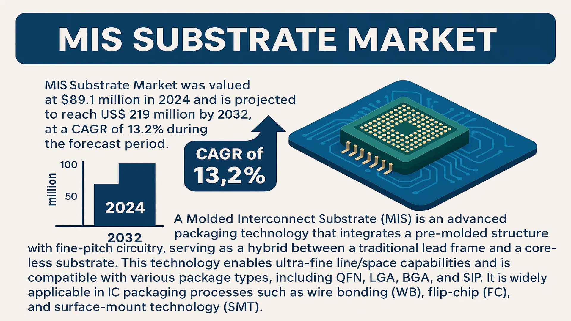
The global MIS Substrate Market was valued at 89.1 million in 2024 and is projected to reach US$ 219 million by 2032, at a CAGR of 13.2% during the forecast period.
A Molded Interconnect Substrate (MIS) is an advanced packaging technology that integrates a pre-molded structure with fine-pitch circuitry, serving as a hybrid between a traditional lead frame and a coreless substrate. This technology enables ultra-fine line/space capabilities and is compatible with various package types, including QFN, LGA, BGA, and SIP. It is widely applicable in IC packaging processes such as wire bonding (WB), flip-chip (FC), and surface-mount technology (SMT).
The market is experiencing robust growth driven by the escalating demand for high-performance, miniaturized electronics in sectors like network communications, automotive electronics, and consumer IoT. The proliferation of 5G infrastructure, electric vehicles, and AIoT devices significantly increases the requirements for semiconductor packaging substrates that offer superior design flexibility, enhanced electrical performance, and high reliability. Key players such as PPt, MiSpak Technology, and QDOS are expanding their multi-layer MIS offerings to meet this sophisticated demand, further propelling market expansion.
MARKET DYNAMICS
MARKET DRIVERS
Rising Demand for Advanced Semiconductor Packaging in 5G and AIoT Applications to Propel Market Growth
The global transition toward 5G infrastructure and AIoT (Artificial Intelligence of Things) devices is significantly driving the adoption of MIS substrates. These advanced packaging solutions offer superior electrical performance, thermal management, and miniaturization capabilities compared to traditional lead-frame and BGA substrates. The 5G infrastructure market is projected to grow substantially, requiring high-frequency, high-power components where MIS substrates excel. Similarly, AIoT applications demand compact, high-reliability packaging for edge computing devices. Major technology companies are investing billions annually in 5G and AI infrastructure development, creating sustained demand for advanced packaging solutions. The ability of MIS substrates to support finer line widths and spaces below 10μm makes them particularly suitable for these high-performance applications where signal integrity and power efficiency are critical.
Expansion of Electric Vehicle and Automotive Electronics Market to Accelerate Adoption
The rapid growth of the electric vehicle market and increasing automotive electronics content are creating substantial opportunities for MIS substrate manufacturers. Modern vehicles incorporate numerous electronic control units, power management systems, and sensor arrays that require robust, reliable packaging solutions. The global electric vehicle market has been growing at approximately 40% annually, with projections indicating continued strong expansion. MIS substrates are particularly valuable in automotive applications due to their excellent thermal performance, reliability under harsh operating conditions, and compatibility with various packaging formats. Power management integrated circuits (PMICs) and motor control units in electric vehicles benefit significantly from the enhanced thermal dissipation and electrical characteristics of MIS substrates. Automotive manufacturers are increasingly specifying these advanced packaging solutions to meet the demanding requirements of next-generation vehicle electronics systems.
Growing Server and Data Center Infrastructure Investments to Drive Market Expansion
Substantial investments in server infrastructure and data centers worldwide are driving demand for high-performance packaging solutions like MIS substrates. The global data center market continues to expand with cloud computing adoption, requiring increasingly powerful and efficient semiconductor packages. MIS substrates enable higher integration density and better thermal management crucial for server processors, networking chips, and power delivery components. Major cloud service providers are investing billions annually in new data center capacity, creating sustained demand for advanced semiconductor packaging. The shift toward higher power densities in computing applications necessitates packaging solutions that can effectively manage heat dissipation while maintaining electrical performance. MIS technology’s ability to provide fine-pitch interconnects and excellent thermal characteristics makes it particularly suitable for these demanding applications.
MARKET CHALLENGES
High Manufacturing Complexity and Cost Constraints Challenge Widespread Adoption
The sophisticated manufacturing processes required for MIS substrates present significant challenges for market expansion. The technology involves complex molding, plating, and patterning processes that require specialized equipment and expertise. Establishing production facilities for multi-layer MIS substrates represents a substantial capital investment, often exceeding traditional packaging infrastructure costs. This high barrier to entry limits the number of qualified suppliers and can create supply chain constraints during periods of high demand. Additionally, the yield optimization for fine-pitch structures remains challenging, particularly for substrates requiring line widths below 15μm. These manufacturing complexities contribute to higher per-unit costs compared to conventional packaging solutions, making price-sensitive applications more difficult to address.
Other Challenges
Limited Manufacturing Capacity and Supply Chain Constraints
The specialized nature of MIS substrate manufacturing has resulted in limited global production capacity concentrated among few suppliers. This concentration creates potential supply chain vulnerabilities, particularly during periods of high semiconductor demand. The lead times for advanced MIS substrates can extend significantly longer than traditional packaging solutions, creating challenges for product planning and time-to-market. The industry faces ongoing challenges in scaling production capacity to meet growing demand while maintaining quality standards and technical specifications.
Technical Standardization and Qualification Hurdles
The relatively new nature of MIS technology means that industry standards and qualification processes are still evolving. This lack of established standards creates challenges for design engineers and procurement specialists evaluating these substrates for their applications. The qualification process for automotive and industrial applications typically requires extensive testing and validation, which can delay adoption timelines. Additionally, the thermal and mechanical performance characteristics differ significantly from traditional substrates, requiring redesign and re-qualification of existing packages.
MARKET RESTRAINTS
Competition from Alternative Advanced Packaging Technologies to Limit Market Penetration
MIS substrates face strong competition from other advanced packaging technologies such as fan-out wafer-level packaging (FOWLP), embedded die substrates, and silicon interposers. These competing technologies have established manufacturing ecosystems and in some cases offer superior performance characteristics for specific applications. The semiconductor packaging industry continues to innovate rapidly, with new approaches emerging regularly. This competitive landscape requires MIS substrate manufacturers to continuously demonstrate technical and economic advantages over alternative solutions. The decision to adopt MIS technology often involves comprehensive technical evaluation and cost-benefit analysis, which can slow adoption rates particularly in applications where existing solutions meet requirements adequately.
Economic Sensitivity and Cost Pressure in Consumer Applications to Restrain Growth
The price sensitivity of consumer electronics applications presents a significant restraint for MIS substrate adoption. While the technology offers performance advantages, the cost premium compared to traditional packaging solutions can be prohibitive for high-volume, cost-sensitive applications. Consumer electronics manufacturers operate on thin margins and often prioritize cost reduction over performance enhancement. This economic reality limits MIS substrate penetration in market segments where performance requirements can be met with less expensive alternatives. The ongoing pressure to reduce semiconductor package costs across the industry creates challenges for advanced technologies that inherently involve higher manufacturing expenses.
Technical Limitations in Ultra-High Frequency Applications to Constrain Market Expansion
While MIS substrates offer excellent performance across many applications, they face limitations in ultra-high frequency scenarios above 100GHz. The material properties and structure of molded interconnect substrates can introduce signal integrity challenges at extremely high frequencies that alternative technologies like thin-film substrates address more effectively. This technical constraint limits MIS substrate adoption in certain RF and millimeter-wave applications where signal loss and impedance control are critical. The development of 6G communications and advanced radar systems requires packaging solutions capable of supporting frequencies beyond current MIS technology limitations, creating opportunities for competing approaches in these specific application areas.
MARKET OPPORTUNITIES
Expansion into Third-Generation Semiconductor Applications to Create New Growth Avenues
The emergence of wide bandgap semiconductors using gallium nitride (GaN) and silicon carbide (SiC) presents significant opportunities for MIS substrate manufacturers. These third-generation semiconductors operate at higher frequencies, temperatures, and power levels than traditional silicon devices, requiring packaging solutions with superior thermal and electrical performance. MIS substrates are particularly well-suited for GaN device packaging, where their thermal management capabilities and high-frequency performance provide distinct advantages. The power semiconductor market is growing rapidly as industries seek more efficient power conversion systems, creating substantial demand for advanced packaging solutions. The ability to support higher operating temperatures and power densities positions MIS technology favorably for these emerging applications.
Geographic Expansion and Manufacturing Capacity Investments to Unlock New Markets
Strategic investments in manufacturing capacity and geographic expansion represent significant growth opportunities for MIS substrate suppliers. Currently, production is concentrated in specific regions, creating opportunities for expansion into new geographic markets to better serve global customers. Several major semiconductor companies are diversifying their supply chains and seeking regional manufacturing capabilities, creating demand for local advanced packaging solutions. Investments in additional production capacity could help address current supply constraints and enable broader market penetration. The establishment of manufacturing facilities in strategic locations could reduce logistics costs and improve responsiveness to customer requirements, particularly for time-sensitive applications.
Development of Multi-layer and Advanced Architecture Solutions to Address Emerging Applications
The ongoing development of more sophisticated multi-layer MIS substrates creates opportunities to address increasingly complex packaging requirements. Applications such as heterogeneous integration, system-in-package (SiP) solutions, and advanced sensor packaging require substrates capable of supporting multiple die types and complex interconnect schemes. The ability to provide 4-layer and 6-layer MIS substrates enables more integrated solutions that can replace multiple discrete packages. This integration capability is particularly valuable in space-constrained applications like mobile devices, wearables, and advanced medical equipment. The continued advancement of MIS technology to support even more layers and finer features will open additional application areas and drive market expansion.
MIS SUBSTRATE MARKET TRENDS
Advancements in Packaging Technology Driving Adoption of MIS Substrates
The global semiconductor packaging industry is undergoing a significant transformation, with Molded Interconnect Substrate (MIS) technology emerging as a critical innovation poised to replace traditional lead-frame packages and BGA substrates. This shift is driven by the superior performance characteristics of MIS, which utilizes build-up technology and breaks away from conventional polymer cores to achieve ultra-fine line/space capabilities. The market, valued at $89.1 million in 2024, is projected to reach $219 million by 2032, growing at a robust CAGR of 13.2%. This growth is largely fueled by the technology’s compatibility with various packaging formats, including QFN, LGA, BGA, and SIP packages, making it applicable across wire bonding, flip-chip, and surface-mount technology processes. The ability to support multi-layer configurations—with key players like PPt offering up to 6 layers—further enhances its appeal for complex, high-performance applications.
Other Trends
Expansion in High-Growth Application Segments
The demand for MIS substrates is being significantly propelled by their adoption in high-growth sectors such as network communication infrastructure, automotive electronics, and AIoT applications. In the automotive sector, the rapid electrification and intelligence of vehicles are driving the need for reliable, high-performance electronic control units, where MIS substrates offer enhanced thermal management and electrical performance. Similarly, the rollout of 5G infrastructure and the expansion of data centers require substrates that can handle higher frequencies and power densities, areas where MIS technology excels. For instance, over 60% of current MIS substrate demand originates from power IC applications, including PMIC and analog devices, highlighting their critical role in energy management systems. Furthermore, the adoption of third-generation semiconductors, particularly GaN devices, is creating new opportunities, as MIS substrates provide the necessary reliability and efficiency for these advanced materials.
Geographic and Competitive Landscape Evolution
The geographic distribution of the MIS substrate market is concentrated primarily in Asia, which accounts for the majority of both production and consumption, driven by strong semiconductor manufacturing ecosystems in Taiwan, China, and Malaysia. Taiwan-based PPt leads the market with its extensive multi-layer product offerings, while MiSpak Technology in China and QDOS in Malaysia focus on 1 to 3-layer variants, catering to diverse customer needs. The competitive landscape is characterized by ongoing innovations in layer complexity and material science, aimed at enhancing product performance and expanding application scope. However, the market also faces challenges such as high initial investment costs and the technical complexity associated with manufacturing multi-layer MIS substrates, which could restrain faster adoption among smaller players. Despite these hurdles, the ongoing miniaturization trend in electronics and the push towards more integrated, high-performance packaging solutions continue to drive R&D investments and strategic collaborations across the industry.
COMPETITIVE LANDSCAPE
Key Industry Players
Companies Focus on Technological Innovation and Capacity Expansion to Maintain Market Leadership
The global Molded Interconnect Substrate (MIS) market exhibits a concentrated competitive structure, dominated by a few specialized manufacturers with significant technological expertise and production capabilities. PPt Corporation (Taiwan) emerges as the undisputed market leader, commanding an estimated revenue share of approximately 42% in 2024. This dominance is primarily attributed to its comprehensive product portfolio, which includes 1-layer to 6-layer MIS substrates, and its pioneering development of multi-layer board windable lead frame products for advanced multi-chip packaging applications.
MiSpak Technology (China) and QDOS (Malaysia) collectively hold a substantial portion of the remaining market share, estimated at around 38%. Both companies have strengthened their positions through strategic focus on high-growth application segments, particularly power ICs and automotive electronics. Their expansion initiatives are closely aligned with the increasing demand from electric vehicle manufacturing and 5G infrastructure deployment.
These leading players are actively engaged in capacity expansion and technological upgrades to cater to the evolving requirements of semiconductor packaging. The market is characterized by intense R&D investment focused on enhancing fine-line/space capabilities and improving thermal performance for high-power applications like GaN devices. Because the technology is still emerging, competition extends beyond traditional substrate manufacturers to include established lead-frame and substrate suppliers who are developing competing solutions.
Meanwhile, several other companies are entering the space or expanding their capabilities, often through partnerships with OEMs in the automotive and networking sectors. These players are strengthening their market presence by focusing on application-specific solutions and securing long-term supply agreements with major semiconductor packaging and testing (OSAT) companies, ensuring their growth trajectory aligns with the overall market expansion.
List of Key MIS Substrate Companies Profiled
- PPt Corporation (Taiwan)
- MiSpak Technology (China)
- QDOS International Sdn Bhd (Malaysia)
Segment Analysis:
By Type
Multi-layer MIS Segment Dominates the Market Due to Superior Performance in High-Density Packaging Applications
The market is segmented based on type into:
- Single-layer MIS
- Multi-layer MIS
- Subtypes: 2-layer, 3-layer, 4-layer, 6-layer, and others
By Application
Power IC Segment Leads Due to Critical Role in Energy Management and High-Voltage Applications
The market is segmented based on application into:
- Power IC
- RF/5G
- Fingerprint Sensor
- OIS (Optical Image Stabilization)
- Others
- Subtypes: Automotive electronics, LED packaging, GaN devices, and third-generation semiconductors
By End-Use Industry
Consumer Electronics Segment Leads Due to High Volume Adoption in Smart Devices and Wearables
The market is segmented based on end-use industry into:
- Consumer Electronics
- Automotive
- Telecommunications
- Industrial
- Others
- Subtypes: Medical devices, aerospace, and defense applications
By Packaging Technology
BGA Packaging Segment Leads Due to Superior Thermal and Electrical Performance in Advanced ICs
The market is segmented based on packaging technology into:
- QFN (Quad Flat No-leads)
- LGA (Land Grid Array)
- BGA (Ball Grid Array)
- SIP (System in Package)
- Others
- Subtypes: WB (Wire Bonding), FC (Flip Chip), and SMT (Surface Mount Technology) compatible packages
Regional Analysis: MIS Substrate Market
Asia-Pacific
The Asia-Pacific region dominates the global MIS Substrate market, accounting for over 65% of total consumption in 2024. This leadership position is driven by the region’s robust semiconductor manufacturing ecosystem, particularly in Taiwan, China, South Korea, and Japan. Taiwan’s semiconductor industry, valued at approximately $150 billion annually, serves as a critical hub for advanced packaging technologies, including MIS substrates. The presence of key manufacturers like PPt in Taiwan and MiSpak Technology in China creates a strong supply chain foundation. Demand is primarily fueled by the massive production of consumer electronics, telecommunications equipment, and automotive electronics across the region. China’s substantial investments in 5G infrastructure and electric vehicle production are creating additional growth opportunities. However, the region faces challenges related to intellectual property protection and varying regulatory standards across different countries.
North America
North America represents a significant and technologically advanced market for MIS substrates, particularly driven by demand from the United States. The region’s market is characterized by high-value applications in data centers, network infrastructure, and automotive electronics. Major technology companies and automotive manufacturers are increasingly adopting MIS substrates for their superior performance in power management and RF applications. The U.S. CHIPS Act, which allocates $52 billion for semiconductor research and manufacturing, is expected to further boost domestic capabilities in advanced packaging technologies including MIS substrates. The region shows strong demand for multi-layer MIS products for complex semiconductor packaging applications, particularly in the defense and aerospace sectors where reliability and performance are critical requirements.
Europe
Europe’s MIS substrate market is growing steadily, supported by the region’s strong automotive industry and increasing investments in telecommunications infrastructure. Germany, as the automotive manufacturing hub of Europe, drives significant demand for MIS substrates used in vehicle electrification and advanced driver assistance systems. The European Union’s focus on technological sovereignty and reduced dependency on Asian semiconductor suppliers is creating opportunities for local development of advanced packaging technologies. Strict environmental regulations under the EU’s RoHS and REACH directives are pushing manufacturers toward more environmentally friendly production processes. The region shows particular strength in research and development activities, with several academic institutions and research centers working on next-generation semiconductor packaging solutions.
South America
The South American market for MIS substrates is in its early development stages, with limited local manufacturing capabilities. Most MIS substrates are imported from Asian manufacturers to serve the region’s growing electronics manufacturing industry. Brazil represents the largest market in the region, driven by its automotive and consumer electronics sectors. The market growth is constrained by economic volatility and limited investment in semiconductor infrastructure. However, increasing digitalization efforts and growing middle-class population are creating gradual demand for electronic devices that incorporate MIS technology. The region primarily consumes single-layer MIS substrates for less complex applications due to cost considerations and technical capability limitations.
Middle East & Africa
The Middle East and Africa region represents an emerging market for MIS substrates, with growth primarily driven by infrastructure development and digital transformation initiatives. Countries like Israel, Saudi Arabia, and the UAE are making significant investments in technology infrastructure, including 5G networks and data centers, which require advanced semiconductor packaging solutions. Israel’s strong technology sector, particularly in cybersecurity and communications, creates specialized demand for high-performance MIS substrates. The region faces challenges related to limited local semiconductor manufacturing and reliance on imports. However, increasing government support for technology development and economic diversification programs in Gulf Cooperation Council countries are creating long-term growth potential for advanced packaging technologies including MIS substrates.
Report Scope
This market research report provides a comprehensive analysis of the global and regional Semiconductor and Electronics markets, covering the forecast period 2025–2032. It offers detailed insights into market dynamics, technological advancements, competitive landscape, and key trends shaping the industry.
Key focus areas of the report include:
- Market Size & Forecast: Historical data and future projections for revenue, unit shipments, and market value across major regions and segments.
- Segmentation Analysis: Detailed breakdown by product type, technology, application, and end-user industry to identify high-growth segments and investment opportunities.
- Regional Outlook: Insights into market performance across North America, Europe, Asia-Pacific, Latin America, and the Middle East & Africa, including country-level analysis where relevant.
- Competitive Landscape: Profiles of leading market participants, including their product offerings, R&D focus, manufacturing capacity, pricing strategies, and recent developments such as mergers, acquisitions, and partnerships.
- Technology Trends & Innovation: Assessment of emerging technologies, integration of AI/IoT, semiconductor design trends, fabrication techniques, and evolving industry standards.
- Market Drivers & Restraints: Evaluation of factors driving market growth along with challenges, supply chain constraints, regulatory issues, and market-entry barriers.
- Stakeholder Analysis: Insights for component suppliers, OEMs, system integrators, investors, and policymakers regarding the evolving ecosystem and strategic opportunities.
Primary and secondary research methods are employed, including interviews with industry experts, data from verified sources, and real-time market intelligence to ensure the accuracy and reliability of the insights presented.
FREQUENTLY ASKED QUESTIONS:
What is the current market size of Global MIS Substrate Market?
-> MIS Substrate Market was valued at 89.1 million in 2024 and is projected to reach US$ 219 million by 2032, at a CAGR of 13.2% during the forecast period.
Which key companies operate in Global MIS Substrate Market?
-> Key players include PPt (Taiwan), MiSpak Technology (China), and QDOS (Malaysia), among others.
What are the key growth drivers?
-> Key growth drivers include demand from network communication products (servers, data centers), automotive electronic control equipment driven by electric vehicles, and the proliferation of 5G and AIoT applications.
Which region dominates the market?
-> Asia-Pacific is the dominant region, driven by manufacturing hubs in Taiwan, China, and Malaysia.
What are the emerging trends?
-> Emerging trends include the shift towards multi-layer MIS substrates for complex multi-chip packaging and increased adoption in third-generation semiconductors like GaN devices.

Get Sample Report PDF for Exclusive Insights
Report Sample Includes
- Table of Contents
- List of Tables & Figures
- Charts, Research Methodology, and more...
 Download Sample Report PDF