MARKET INSIGHTS
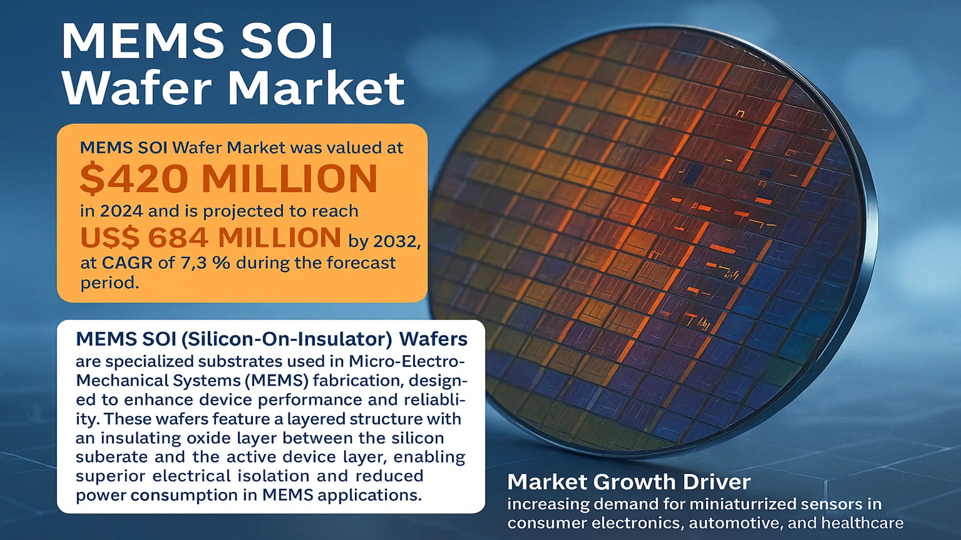
The global MEMS SOI Wafer Market was valued at 420 million in 2024 and is projected to reach US$ 684 million by 2032, at a CAGR of 7.3% during the forecast period.
MEMS SOI (Silicon-On-Insulator) Wafers are specialized substrates used in Micro-Electro-Mechanical Systems (MEMS) fabrication, designed to enhance device performance and reliability. These wafers feature a layered structure with an insulating oxide layer between the silicon substrate and the active device layer, enabling superior electrical isolation and reduced power consumption in MEMS applications.
The market growth is driven by increasing demand for miniaturized sensors in consumer electronics, automotive, and healthcare applications. While 150mm wafers currently dominate, the shift toward 200mm and 300mm wafers is gaining momentum to accommodate larger production volumes. Key players like Soitec, Shin-Etsu, and SUMCO collectively hold significant market share, with ongoing innovations in wafer bonding techniques and material quality improvements further propelling industry expansion.
MARKET DYNAMICS
MARKET DRIVERS
Expansion of IoT and Smart Devices Fuels MEMS SOI Wafer Demand
The rapid proliferation of Internet of Things (IoT) devices and smart technologies is creating substantial demand for MEMS components fabricated on SOI wafers. With over 30 billion IoT devices projected to be in operation globally by 2025, manufacturers are increasingly turning to SOI technology for its superior performance in sensor applications. MEMS SOI wafers offer distinct advantages in terms of reduced power consumption and improved signal integrity – critical factors for battery-operated smart devices. The automotive sector particularly benefits from these characteristics, with advanced driver assistance systems (ADAS) requiring high-reliability MEMS sensors that SOI wafers can reliably deliver.
5G Network Rollouts Accelerate RF MEMS Adoption
Global 5G infrastructure deployment is driving unprecedented demand for RF MEMS components built on SOI substrates. The transition to higher frequency bands in 5G networks necessitates components with exceptional linearity and low insertion loss – characteristics that SOI wafers inherently provide. Major telecommunications equipment providers are increasingly specifying SOI-based RF switches and filters for base stations and mobile devices. With 5G subscriptions expected to surpass 2 billion worldwide in the next three years, this represents a significant growth vector for MEMS SOI wafer manufacturers. The technology’s ability to integrate multiple RF functions on a single chip while maintaining performance isolation makes it particularly valuable for 5G applications.
➤ The automotive MEMS sensor market, a key application area for SOI wafers, is projected to maintain a growth rate exceeding 8% annually through 2030, driven by increasing vehicle electrification and autonomous driving capabilities.
Medical Device Miniaturization Creates New Opportunities
Advancements in minimally invasive medical technologies are creating robust demand for ultra-compact MEMS devices fabricated on SOI wafers. The medical sector requires components with unmatched reliability and precision, making SOI’s excellent electrical isolation and reduced parasitic effects particularly valuable. Implantable devices, diagnostic equipment, and surgical tools increasingly incorporate MEMS pressure sensors, accelerometers, and microfluidics that benefit from SOI technology. With the global medical device market growing at approximately 6% annually, this represents a stable, high-value application segment for MEMS SOI wafers.
MARKET RESTRAINTS
High Manufacturing Costs Constrain Market Penetration
While offering superior performance characteristics, MEMS SOI wafers carry significantly higher production costs compared to conventional silicon substrates. The specialized fabrication processes required for SOI, including smart cut technology and wafer bonding, contribute to costs that can be 30-50% higher than bulk silicon alternatives. This price premium limits adoption in cost-sensitive consumer electronics applications, where manufacturers often opt for conventional MEMS solutions despite performance compromises. The capital-intensive nature of SOI wafer production also creates barriers to entry for new market participants, potentially restricting competition and innovation.
Complex Supply Chain Creates Vulnerabilities
The MEMS SOI wafer ecosystem involves multiple specialized players across substrate preparation, device fabrication, and packaging – creating potential bottlenecks in the supply chain. Recent global disruptions have highlighted the fragility of this interconnected network, with lead times for certain SOI wafer types extending beyond six months in some cases. The industry’s reliance on a limited number of substrate suppliers further exacerbates supply risks, as does the concentration of advanced MEMS manufacturing capacity in specific geographic regions. These complexities pose significant challenges for device manufacturers requiring consistent, predictable wafer supply to meet production schedules.
MARKET OPPORTUNITIES
Emerging Photonics Applications Open New Frontiers
The convergence of MEMS and photonic technologies is creating exciting opportunities for SOI wafer providers. Silicon photonics systems increasingly incorporate MEMS components for light modulation and beam steering, leveraging SOI’s excellent optical properties. This hybrid approach is gaining traction in LiDAR systems for autonomous vehicles, optical communications equipment, and biomedical imaging devices. The market for photonic integrated circuits is expanding rapidly, with annual growth rates exceeding 20%, representing a significant greenfield opportunity for MEMS SOI wafer manufacturers able to meet the unique requirements of photonic applications.
Advanced Packaging Technologies Enhance Value Proposition
Innovations in 3D integration and heterogeneous packaging are creating new possibilities for MEMS SOI devices. These advanced packaging approaches allow for tighter integration of MEMS with complementary CMOS circuitry, improving system performance while reducing footprint. SOI wafers play a critical role in these architectures by providing excellent isolation between stacked die. The development of through-SOI-via (TSV) technology further enhances integration possibilities, enabling more compact and power-efficient device designs across automotive, aerospace, and industrial applications.
MARKET CHALLENGES
Intellectual Property Complexities Create Barriers
The MEMS SOI wafer landscape is characterized by a dense web of overlapping patents and proprietary technologies, creating potential legal and operational hurdles. Companies developing new SOI-based MEMS solutions often navigate complex licensing agreements and face potential infringement risks. This intellectual property environment can slow innovation cycles and increase development costs, particularly for smaller players lacking extensive patent portfolios. The situation is further complicated by differing international IP regimes, adding complexity to global market strategies.
Workforce Shortages Threaten Growth Momentum
The specialized nature of MEMS SOI technology creates acute demand for engineers with expertise in materials science, semiconductor physics, and microfabrication techniques. However, educational institutions are struggling to produce sufficient graduates with these niche skill sets, leading to intense competition for qualified personnel. The problem is particularly acute in regions experiencing rapid semiconductor industry growth, where multiple companies are vying for the same limited talent pool. This skills gap threatens to constrain capacity expansion and innovation across the MEMS SOI wafer ecosystem.
MEMS SOI WAFER MARKET TRENDS
Increasing Adoption of MEMS SOI Wafers in IoT and 5G Applications
The proliferation of Internet of Things (IoT) devices and the rapid deployment of 5G networks are significantly driving the demand for MEMS SOI wafers. These wafers are preferred due to their superior electrical isolation and reduced power consumption, which are critical for high-frequency RF applications. The global market for MEMS SOI wafers is expected to grow at a CAGR of 7.3% from 2024 to 2032, reaching $684 million by 2032. Furthermore, the increasing need for miniaturized sensors in smart devices and wearables is accelerating the adoption of MEMS-based solutions, particularly in the consumer electronics and automotive sectors.
Other Trends
Advancements in Wafer Manufacturing Technologies
Innovations in wafer fabrication techniques, such as thin-film SOI and advanced bonding processes, are enhancing the performance and yield of MEMS SOI wafers. Leading manufacturers, including Soitec and Shin-Etsu, are investing heavily in R&D to improve wafer quality while reducing production costs. The 200 mm and 300 mm wafer segments are witnessing increased adoption due to their cost-efficiency and compatibility with existing semiconductor fabrication facilities. Additionally, new developments in etching and polishing technologies are enabling higher precision in MEMS device manufacturing, further boosting market growth.
Expansion of Automotive MEMS Applications
The automotive industry is emerging as a key driver for the MEMS SOI wafer market, particularly with the rise of autonomous driving systems and electric vehicles (EVs). MEMS-based sensors, such as accelerometers and gyroscopes, are essential for advanced driver-assistance systems (ADAS) and vehicle stability control. The shift towards silicon-on-insulator (SOI) technology in these applications is due to its superior thermal stability and reduced signal interference. With the global automotive MEMS market projected to grow steadily, demand for high-performance SOI wafers is expected to rise, especially in regions like North America and Asia-Pacific where automotive innovation is accelerating.
COMPETITIVE LANDSCAPE
Key Industry Players
Technological Innovation and Strategic Expansion Define Market Leadership
The global MEMS SOI wafer market features a competitive but consolidated landscape, with Soitec and Shin-Etsu emerging as dominant players, collectively accounting for approximately 30% of the market revenue in 2024. These companies maintain their leadership through continuous R&D investments in advanced wafer technologies, particularly for MEMS and RF applications. Their strong manufacturing capabilities and strategic partnerships with semiconductor giants solidify their market positions.
Emerging players like SUMCO and GlobalWafers are gaining traction through aggressive capacity expansions in Asia-Pacific markets. While SUMCO focuses on optimizing production yields for 200mm SOI wafers—highly demanded for automotive MEMS sensors—GlobalWafers has recently expanded its SOI production lines in Taiwan to cater to growing RF-SOI demand from 5G component manufacturers. This regional focus allows them to compete effectively against larger incumbents.
Meanwhile, NSIG (Okmetic) and IceMos Technology differentiate themselves through specialized SOI solutions. NSIG, for instance, has developed ultra-thin SOI wafers with enhanced thermal properties for high-power MEMS applications, while IceMos specializes in cost-effective SOI substrates for consumer electronics. Such product specialization enables these mid-size players to carve out profitable niches despite intense competition.
List of Key MEMS SOI Wafer Manufacturers Profiled
- Soitec (France)
- Shin-Etsu Chemical Co., Ltd. (Japan)
- SUMCO Corporation (Japan)
- GlobalWafers Co., Ltd. (Taiwan)
- NSIG (Okmetic) (Finland)
- IceMos Technology (UK)
- Wafer Works Corporation (Taiwan)
- Shenyang Silicon Technology (China)
- Zhonghuan Advanced Semiconductor (China)
- Shanghai Advanced Silicon Technology (China)
- WaferPro (U.S.)
Segment Analysis:
By Type
150mm and Below Segment Leads Due to Cost-Effectiveness in Small-Scale MEMS Production
The market is segmented based on type into:
- 150mm and Below
- 200 mm
- 300 mm
By Application
MEMS Segment Dominates Owing to Increasing Demand for Miniaturized Sensors and Actuators
The market is segmented based on application into:
- Power Devices
- MEMS
- RF Devices
- Optoelectronic Devices
- Others
By Thickness
Thin Film SOI Wafers Gain Traction for Compact Device Designs
The market is segmented based on thickness into:
- Thin Film SOI
- Thick Film SOI
By End-User Industry
Consumer Electronics Contributes Significantly to Market Growth
The market is segmented based on end-user industry into:
- Consumer Electronics
- Automotive
- Healthcare
- Industrial
- Telecommunications
Regional Analysis: MEMS SOI Wafer Market
Asia-Pacific
The Asia-Pacific (APAC) region dominates the MEMS SOI Wafer market, holding the largest revenue share globally. This growth is driven by rapid industrialization, expanding semiconductor manufacturing, and increasing adoption of MEMS-based devices in consumer electronics, automotive, and telecommunications. China and Japan are the primary contributors, with China alone accounting for over 40% of the region’s wafer production capacity. The surge in demand for 200mm and 300mm wafers in MEMS applications, such as sensors and RF devices, further fuels market expansion. Local players like Shin-Etsu and SUMCO have heavily invested in SOI wafer production to meet rising domestic and international demand.
North America
North America is a key innovator in MEMS SOI wafer technology, propelled by strong R&D investments and high demand for advanced MEMS applications in aerospace, medical devices, and IoT. The U.S. leads the region, with major technology hubs like Silicon Valley driving semiconductor innovation. Regulatory support, including funding under initiatives like the CHIPS Act, bolsters domestic manufacturing capabilities. Soitec and GlobalWafers have a significant presence here, offering high-performance wafers for RF and optoelectronic applications. However, higher production costs compared to Asia remain a challenge for widespread adoption among cost-sensitive industries.
Europe
Europe’s market is characterized by strict technological standards and sustainability initiatives, particularly in automotive and industrial automation. Germany and France are central to demand growth, with major automakers integrating MEMS-based sensors for advanced driver-assistance systems (ADAS) and electrification. Soitec (France) and Okmetic (Finland) lead regional production, emphasizing energy-efficient wafer solutions compliant with EU regulations. While the region lags behind Asia in volume production, its focus on high-margin, specialized wafers for niche applications ensures steady growth.
South America
The South American market for MEMS SOI wafers is nascent but emerging, with Brazil and Argentina as the primary demand centers. The region faces challenges such as limited semiconductor infrastructure and reliance on imports from Asia and North America. However, increasing investments in telecommunications and automotive electronics present opportunities. Economic volatility and lack of local manufacturing expertise hinder faster adoption, but partnerships with global suppliers could spur future development.
Middle East & Africa
The MEMS SOI wafer market in MEA is in its early stages, with growth primarily driven by telecom infrastructure projects and oil & gas sensor applications. Countries like Israel and Saudi Arabia are investing in semiconductor R&D, but local production remains minimal. The region relies heavily on imports from Asia and Europe, with demand concentrated in defense and industrial applications. While long-term potential exists due to diversification efforts, limited funding and weak supply chains slow market progression.
Report Scope
This market research report provides a comprehensive analysis of the Global MEMS SOI Wafer Market, covering the forecast period 2024–2032. It offers detailed insights into market dynamics, technological advancements, competitive landscape, and key trends shaping the industry.
Key focus areas of the report include:
- Market Size & Forecast: Historical data and future projections for revenue, unit shipments, and market value across major regions and segments. The global MEMS SOI Wafer market was valued at USD 420 million in 2024 and is projected to reach USD 684 million by 2032, growing at a CAGR of 7.3%.
- Segmentation Analysis: Detailed breakdown by wafer size (150mm and below, 200mm, 300mm) and application (Power Devices, MEMS, RF Devices, Optoelectronic Devices, Others) to identify high-growth segments.
- Regional Outlook: Insights into market performance across North America, Europe, Asia-Pacific, Latin America, and Middle East & Africa. The U.S. and China are key growth markets.
- Competitive Landscape: Profiles of leading manufacturers including Soitec, Shin-Etsu, SUMCO, GlobalWafers, and NSIG (Okmetic), covering their market share, product portfolios, and strategic initiatives.
- Technology Trends & Innovation: Assessment of advanced fabrication techniques, emerging MEMS applications, and material innovations in SOI wafer technology.
- Market Drivers & Restraints: Evaluation of factors such as growing demand for IoT devices, automotive MEMS applications, and semiconductor industry growth, along with supply chain challenges.
- Stakeholder Analysis: Strategic insights for wafer manufacturers, semiconductor companies, foundries, and investors regarding market opportunities and challenges.
The research employs both primary and secondary methodologies, including interviews with industry experts and analysis of verified market data to ensure accuracy and reliability.
FREQUENTLY ASKED QUESTIONS:
What is the current market size of Global MEMS SOI Wafer Market?
-> MEMS SOI Wafer Market was valued at 420 million in 2024 and is projected to reach US$ 684 million by 2032, at a CAGR of 7.3% during the forecast period.
Which key companies operate in Global MEMS SOI Wafer Market?
-> Key players include Soitec, Shin-Etsu, SUMCO, GlobalWafers, NSIG (Okmetic), IceMos Technology, Wafer Works Corporation, and Shenyang Silicon Technology.
What are the key growth drivers?
-> Key growth drivers include rising demand for MEMS in consumer electronics and automotive applications, increasing adoption of IoT devices, and advancements in semiconductor manufacturing technologies.
Which region dominates the market?
-> Asia-Pacific is the largest market, driven by semiconductor manufacturing in China, Japan, and South Korea, while North America leads in technological innovation.
What are the emerging trends?
-> Emerging trends include development of larger wafer sizes (300mm), integration of AI in MEMS fabrication, and increasing demand for RF-SOI wafers in 5G applications.

Get Sample Report PDF for Exclusive Insights
Report Sample Includes
- Table of Contents
- List of Tables & Figures
- Charts, Research Methodology, and more...