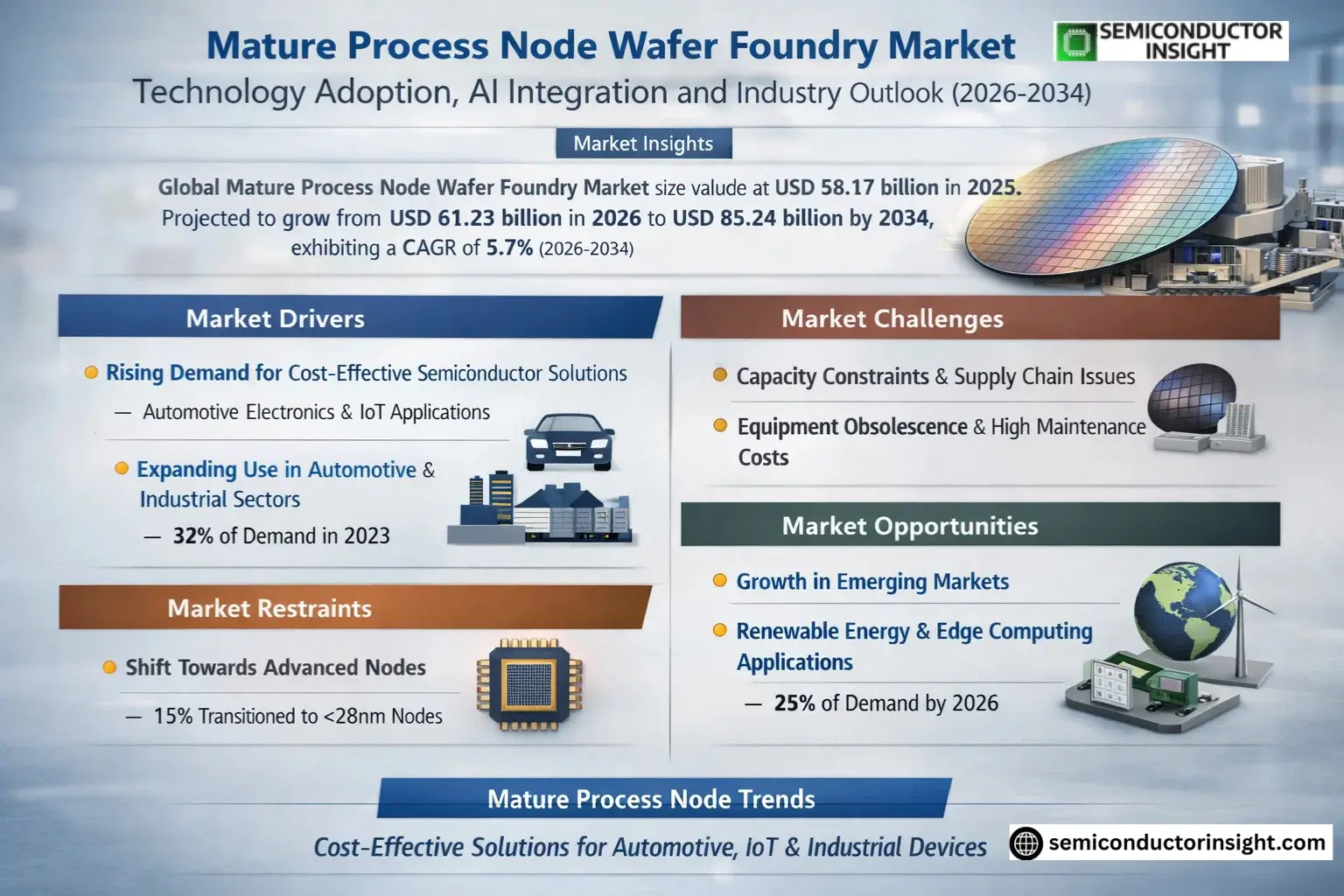
Market Insights
Global Mature Process Node Wafer Foundry Market size was valued at USD 58.17 billion in 2025. The market is projected to grow from USD 61.23 billion in 2026 to USD 85.24 billion by 2034, exhibiting a CAGR of 5.7% during the forecast period.
Mature process node wafer foundries specialize in semiconductor manufacturing using established fabrication technologies, typically ranging from 28nm to above 0.25µm nodes. These nodes remain critical for cost-sensitive applications such as automotive electronics, IoT devices, and industrial controllers where cutting-edge performance isn’t required but reliability and affordability are paramount.
The sustained demand stems from several factors including the proliferation of connected devices requiring legacy chips, automotive electrification trends needing robust components, and supply chain diversification efforts post-pandemic. Leading foundries like TSMC and Samsung continue investing in mature node capacity expansions while smaller players focus on specialized applications, creating a dynamic competitive landscape across different process generations.
MARKET DRIVERS
Growing Demand for Cost-Effective Semiconductor Solutions
Mature Process Node Wafer Foundry Market is experiencing strong growth due to increasing demand for affordable semiconductor solutions. With many industries focused on optimizing costs, mature nodes (28nm and above) offer a balance between performance and economic efficiency. The automotive and IoT sectors, in particular, are driving demand as they don’t always require cutting-edge process technologies.
Expanding Applications in Automotive and Industrial Sectors
Automotive electronics and industrial automation systems are increasingly adopting mature process node chips for their reliability and proven manufacturing processes. These sectors accounted for approximately 32% of mature node wafer demand in 2023, with steady annual growth projected.
Foundries specializing in mature nodes are benefiting from long product lifecycles and established design ecosystems, creating stable revenue streams compared to leading-edge nodes.
MARKET CHALLENGES
Capacity Constraints and Supply Chain Pressures
While demand grows, the Mature Process Node Wafer Foundry Market faces capacity constraints as many fabs prioritize advanced nodes. The consolidation of mature node capacity among fewer foundries has created supply bottlenecks, particularly for 40nm-65nm nodes used in automotive applications.
Other Challenges
Equipment Obsolescence and Maintenance Costs
Maintaining aging semiconductor equipment for mature nodes requires significant investment, with maintenance costs increasing by an average of 7-9% annually across the industry.
Design Complexity at Older Nodes
Developing new products on mature process nodes often requires creative design solutions to meet modern performance requirements, adding to development timelines.
MARKET RESTRAINTS
Shift Towards Advanced Nodes for High-Performance Applications
The gradual migration of certain applications to more advanced nodes creates pressure on the Mature Process Node Wafer Foundry Market. While the shift affects primarily compute-intensive applications, it reduces the total available market for traditional foundry services. Approximately 15% of designs previously using mature nodes have transitioned to <28nm processes in the last three years.
MARKET OPPORTUNITIES
Expansion in Emerging Markets and Applications
Mature Process Node Wafer Foundry Market has significant growth potential in emerging economies where cost sensitivity drives semiconductor adoption. Additionally, new applications in renewable energy systems and edge computing devices are creating fresh demand for reliable, economical mature node solutions. Analysts project these segments will account for 25% of mature node wafer demand by 2026.
Mature Process Node Wafer Foundry Market TrendsGrowing Demand for Cost-Effective Semiconductor Solutions
Mature Process Node Wafer Foundry Market is witnessing steady growth as industries prioritize cost optimization without compromising performance. Mature nodes (28nm and above) continue to dominate production for applications like automotive MCUs, IoT devices, and industrial controllers where cutting-edge nodes aren’t economically viable. Foundries are expanding capacity to meet rising demand from consumer electronics and automotive sectors.
Other Trends
Technology Migration Patterns
While leading foundries focus on advanced nodes below 10nm, many fabless companies are redesigning products to leverage mature nodes’ cost and reliability advantages. This has created a resurgence in 28nm and 40/45nm process adoption, particularly for automotive and industrial applications requiring proven technologies with established supply chains.
Geographical Market Shifts
Asia Pacific maintains dominance in Mature Process Node Wafer Foundry production with TSMC, UMC, and SMIC leading capacity expansions. However, geopolitical factors are driving diversification, with North America and Europe increasing investments in mature node foundries to ensure supply chain security. Governments are offering incentives to bolster domestic semiconductor manufacturing capabilities.
Competitive Landscape Evolution
The market remains concentrated among top players, but emerging foundries are gaining traction through specialized offerings. Companies are differentiating through value-added services like customized IP blocks, faster prototyping, and specialized process optimizations for target applications. This fragmentation creates competitive pricing pressure while expanding customer options.
Application-Specific Process Development
Foundries are increasingly tailoring mature node processes for specific verticals. For automotive applications, enhanced reliability and extended temperature ranges are prioritized. IoT devices benefit from ultra-low power optimizations at mature nodes, while industrial applications demand mixed-signal and high-voltage capabilities. This specialization drives innovation within established process technologies.
COMPETITIVE LANDSCAPE
Key Industry Players
Market Dominated by Established Foundries with Niche Specialists Gaining Traction
Mature Process Node Wafer Foundry Market is led by TSMC, Samsung Foundry, and GlobalFoundries, which collectively hold over 60% market share. These leaders specialize in 28nm to 180nm nodes, serving automotive, IoT, and industrial applications. TSMC maintains technology leadership with its 28nm RF and embedded flash processes, while Samsung leverages its 45nm BCD and CIS capabilities.
Second-tier players like UMC, SMIC, and Tower Semiconductor focus on cost-optimized 65nm-180nm nodes for consumer electronics. Emerging Chinese foundries (Hua Hong, HLMC) are aggressively expanding 90nm-0.18µm capacity. Specialty foundries such as X-FAB (analog/mixed-signal) and SkyWater (government contracts) carve out profitable niches in the fragmented 200mm wafer market.
List of Key Mature Process Node Wafer Foundry Companies Profiled
- TSMC (Taiwan Semiconductor Manufacturing Company)
- Samsung Foundry
- GlobalFoundries
- United Microelectronics Corporation (UMC)
- SMIC (Semiconductor Manufacturing International Corporation)
- Tower Semiconductor
- PSMC (Powerchip Semiconductor Manufacturing Corporation)
- VIS (Vanguard International Semiconductor)
- Hua Hong Semiconductor
- HLMC (Huahong Grace Semiconductor Manufacturing)
- X-FAB
- DB HiTek
- Nexchip
- Intel Foundry Services (IFS)
- SkyWater Technology
Segment Analysis:
| Segment Category | Sub-Segments | Key Insights |
| By Type |
|
28nm Segment dominates due to its ideal balance of cost and performance:
|
| By Application |
|
Automotive Sector shows strongest growth potential:
|
| By End User |
|
Fabless Semiconductor Companies drive majority of demand:
|
| By Technology Node Adoption |
|
Mainstream Migration Nodes represent strategic focus areas:
|
| By Foundry Specialization |
|
Pure-Play Foundries lead in mature node capacity:
|
Regional Analysis: Mature Process Node Wafer Foundry Market
Taiwan maintains unmatched expertise in mature node wafer production through TSMC’s technology leadership and UMC’s specialty process focus. The island’s comprehensive supply chain enables efficient manufacturing of legacy chips for automotive and industrial applications.
Chinese foundries like SMIC and Hua Hong Semiconductor are rapidly expanding mature node capacity to reduce import dependence. Government subsidies and local equipment development programs support this expansion despite geopolitical challenges affecting advanced nodes.
Japan focuses on high-reliability mature nodes for automotive and industrial applications through foundries like Tower Semiconductor. The country’s materials science expertise enables unique process enhancements for legacy technology nodes.
Singapore and Malaysia are emerging as important nodes for mature process manufacturing, attracting investments from global IDMs converting to foundry models. Strategic geographic location provides supply chain resilience for legacy semiconductor production.
North America
North America maintains a strategic position in the Mature Process Node Wafer Foundry Market through specialized analog and mixed-signal production. The region benefits from strong automotive and aerospace industries that require reliable legacy nodes. US-based GlobalFoundries has repositioned as a leader in mature and specialty nodes, while Canada’s semiconductor research institutes contribute to process innovations. The CHIPS Act provisions are beginning to support mature node capacity expansion in the US alongside advanced node investments.
Europe
European semiconductor companies focus on mature process nodes for automotive, industrial, and medical applications. The region’s foundry landscape features specialized players like X-FAB that excel in analog, power, and MEMS technologies on legacy nodes. EU initiatives increasingly recognize the strategic importance of maintaining mature node manufacturing capabilities alongside cutting-edge R&D projects.
South America
South America shows nascent development in mature node semiconductor manufacturing, primarily serving local consumer electronics and automotive markets. Brazil’s CEITEC represents the region’s most significant foundry operation, though scale remains limited compared to other regions. The market potential is growing as regional governments consider semiconductor self-sufficiency initiatives.
Middle East & Africa
The Middle East is emerging as a potential hub for mature node wafer production through strategic investments in semiconductor manufacturing. Israel’s Tower Semiconductor (now part of Intel) provides advanced analog capabilities, while Gulf nations explore semiconductor industrialization plans. Africa’s market remains embryonic but shows increasing demand for legacy node chips in consumer electronics.
Report Scope
This market research report provides a comprehensive analysis of the Mature Process Node Wafer Foundry Market , covering the forecast period 2025–2034. It offers detailed insights into market dynamics, technological advancements, competitive landscape, and key trends shaping the industry.
Key focus areas of the report include:
- Market Overview: The report begins with an overview outlining its current market scenario, key growth indicators, and industry transformation drivers. It discusses macroeconomic factors, demand–supply balance, regulatory landscape, and the strategic role of semiconductors in powering advancements across industries such as automotive, telecommunications, consumer electronics, and industrial automation.
- Market Size & Forecast: Historical data and future projections for revenue, unit shipments, and market value across major regions and segments.
- Segmentation Analysis: Detailed breakdown by product type, technology, application, and end-user industry to identify high-growth segments and investment opportunities.
- Regional Insights: Insights into market performance across North America, Europe, Asia-Pacific, Latin America, and the Middle East & Africa, including country-level analysis where relevant.
- Competitive Landscape: Profiles of leading market participants, including their product offerings, R&D focus, manufacturing capacity, pricing strategies, and recent developments such as mergers, acquisitions, and partnerships.
- Technology Trends & Innovation: Assessment of emerging technologies, integration of AI/IoT, semiconductor design trends, fabrication techniques, and evolving industry standards.
- Market Drivers & Restraints: Evaluation of factors driving market growth along with challenges, supply chain constraints, regulatory issues, and market-entry barriers.
- Stakeholder Insights: Insights for component suppliers, OEMs, system integrators, investors, and policymakers regarding the evolving ecosystem and strategic opportunities.
Primary and secondary research methods are employed, including interviews with industry experts, data from verified sources, and real-time market intelligence to ensure the accuracy and reliability of the insights presented.
FREQUENTLY ASKED QUESTIONS:
What is the current market size of Mature Process Node Wafer Foundry Market?
-> Mature Process Node Wafer Foundry Market size was valued at USD 58.17 billion in 2025. The market is projected to grow from USD 61.23 billion in 2026 to USD 85.24 billion by 2034, exhibiting a CAGR of 5.7% during the forecast period.
Which key companies operate in Mature Process Node Wafer Foundry Market?
-> Key players include TSMC, Samsung Foundry, GlobalFoundries, United Microelectronics Corporation (UMC), SMIC, Tower Semiconductor, PSMC, VIS (Vanguard International Semiconductor), Hua Hong Semiconductor, HLMC, among others.
What are the key growth drivers?
-> Key growth drivers include increasing demand for semiconductors in consumer electronics, automotive applications, industrial automation, and IoT devices.
Which region dominates the market?
-> Asia leads the market, with China, Japan and South Korea being major contributors, while North America remains a significant market.
What are the main process node segments?
-> The market is segmented by process node into 28nm, 40/45nm, 65nm, 90nm, 0.11/0.13micron, 0.15/0.18 micron, and above 0.25 micron.
Get Sample Report PDF for Exclusive Insights
Report Sample Includes
- Table of Contents
- List of Tables & Figures
- Charts, Research Methodology, and more...


