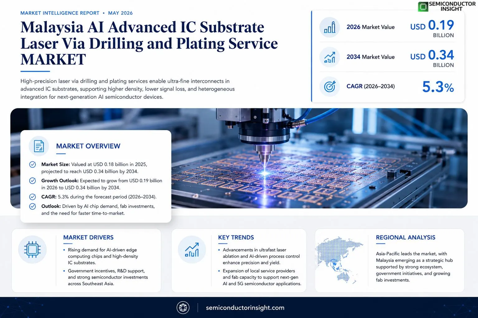
Malaysia AI Advanced IC Substrate Laser Via Drilling and Plating Service Market Insights
Malaysia AI Advanced IC Substrate Laser Via Drilling and Plating Service market size was valued at USD 0.18 billion in 2025. The market is projected to grow from USD 0.19 billion in 2026 to USD 0.34 billion by 2034, exhibiting a CAGR of 5.3% during the forecast period.
Laser via drilling and plating services involve high‑precision laser ablation to create micro‑vias in advanced IC substrates, followed by electro‑plating to fill these vias with conductive material. This process enables higher interconnect density, reduced signal loss, and supports heterogeneous integration required for AI‑enabled semiconductor devices.The market is gaining momentum due to rising demand for AI‑driven edge computing chips, increased investment in semiconductor fabs across Southeast Asia, and the need for faster time‑to‑market for high‑performance packages. Leading providers such as ASE Technology Holding, Amkor Technology, and STATS ChipPAC are expanding their capabilities in Malaysia to meet regional OEM requirements.
MARKET DRIVERS
Rising Demand for High‑Performance IC Substrates
The proliferation of AI‑enabled devices in Malaysia is accelerating the need for advanced IC substrates with fine‑pitch interconnects. Companies are increasingly adopting laser via drilling to achieve sub‑micron vias, which enhances signal integrity for AI processors. Manufacturers are investing heavily in state‑of‑the‑art plating services to meet these performance requirements.
Government Incentives and R&D Support
Malaysia’s strategic initiatives, such as the Digital Economy Blueprint, provide tax incentives and grants for semiconductor‑related R&D. These policies lower the cost of capital for firms establishing laser via drilling facilities, thereby boosting market expansion. Local talent pipelines are also strengthening as universities align curricula with industry needs.
➤ “The integration of AI workloads drives a 12% annual increase in demand for precision‑drilled IC substrates across the region.”
Furthermore, cross‑border collaborations with Taiwanese and Japanese equipment suppliers are facilitating technology transfer, leading to shorter cycle times and higher yields. This collaborative ecosystem is a pivotal catalyst for Malaysia AI Advanced IC Substrate Laser Via Drilling and Plating Service Market.
MARKET CHALLENGES
Skilled Workforce Shortage
Despite government efforts, the pool of engineers proficient in ultra‑precision laser processing remains limited. Companies often have to recruit overseas experts or invest extensively in training programs, which raises operational costs and can delay project timelines.
Other Challenges
High Capital Expenditure
The acquisition of next‑generation laser drilling systems and plating lines requires multi‑million‑ringgit investments. For smaller fab players, securing financing can be difficult, leading to consolidation pressure within the market.
MARKET RESTRAINTS
Stringent Environmental Regulations
Malaysia’s tightening environmental standards for chemical plating processes impose additional compliance costs. Firms must implement advanced waste‑water treatment and adopt eco‑friendly plating chemistries, which can increase production overhead.The need to comply with RoHS and REACH directives further constrains raw material choices, limiting the availability of certain high‑performance plating solutions.Consequently, manufacturers face a balancing act between meeting regulatory demands and maintaining cost‑effective production, which can restrict market entry for new players.
MARKET OPPORTUNITIES
Expansion into Edge‑AI and 5G Infrastructure
Rapid deployment of 5G networks and edge‑computing nodes in Malaysia creates a sizable demand for compact, high‑speed AI chips. These applications require ultra‑reliable via drilling and plating to achieve low latency and high bandwidth, opening new revenue streams for service providers.Emerging sectors such as autonomous vehicles and smart manufacturing also rely on AI‑centric ICs, driving the need for customized substrate solutions that can be delivered through specialized laser via drilling services.Investors are showing heightened interest in joint ventures that combine local market knowledge with foreign technological expertise, presenting a strategic growth avenue for Malaysia AI Advanced IC Substrate Laser Via Drilling and Plating Service Market.
Malaysia AI Advanced IC Substrate Laser Via Drilling and Plating Service Market Trends
Growing Demand for AI‑Enabled Edge Chips
Malaysia AI Advanced IC Substrate Laser Via Drilling and Plating Service Market is being driven by a surge in demand for AI‑enabled edge computing chips. Customers require higher interconnect density and lower signal loss, prompting semiconductor manufacturers to adopt laser‑via drilling paired with electro‑plating for advanced IC substrates. This combination supports heterogeneous integration, enabling compact, high‑performance packages that meet the latency constraints of edge AI workloads. In addition, the shift toward 2.5‑D and 3‑D packaging architectures has raised the importance of precise micro‑via formation, positioning laser‑via services as a critical enabler for next‑generation AI silicon. OEMs in Malaysia are increasingly integrating these services into their design‑for‑manufacturing workflows, reducing cycle time and improving yield consistency. The convergence of local talent pools in photonics and advanced packaging further reinforces the region’s capability to sustain this growth trajectory. Consequently, Malaysia AI Advanced IC Substrate Laser Via Drilling and Plating Service Market is expected to solidify its role as a strategic component of the semiconductor supply chain. Additionally, the rise of local AI startups is prompting rapid prototyping cycles, which rely heavily on fast and accurate via drilling services.
Other Trends
Regional Fab Investments and Provider Expansion
Several major semiconductor fabs have announced new or expanded facilities in Malaysia, reflecting a broader Southeast Asian investment trend. Companies such as ASE Technology Holding, Amkor Technology, and STATS ChipPAC have scaled their laser‑via drilling and plating lines to accommodate local demand. These expansions are supported by government incentives that lower capital costs for high‑precision equipment. As a result, capacity utilization rates have risen to above 80 percent, enabling faster turnaround for AI‑centric designs. The proximity of these service providers to design houses shortens logistics, further encouraging OEMs to adopt advanced IC substrate solutions within Malaysia. The upgraded facilities also incorporate real‑time metrology, ensuring that via dimensions meet the stringent tolerances required by next‑gen AI modules.
Technology Innovation and Outlook
Continuous improvements in ultrafast laser sources and closed‑loop plating control are raising the precision of micro‑via creation to sub‑10‑micron dimensions. These advances lower defect rates and improve electrical performance, which are critical for high‑bandwidth AI accelerators. Collaborative research programs between Malaysian universities and industry players are delivering next‑generation photonic‑mask techniques that further reduce cycle time. While supply constraints for high‑purity copper and specialty gases persist, the localized service ecosystem mitigates bottlenecks by maintaining inventory buffers. Looking ahead, Malaysia AI Advanced IC Substrate Laser Via Drilling and Plating Service Market is poised to benefit from increasing adoption of heterogeneous integration strategies, driving demand for reliable, high‑density interconnect solutions across automotive, IoT, and data‑center segments.
COMPETITIVE LANDSCAPE
Key Industry Players
Malaysia AI Advanced IC Substrate Laser Via Drilling and Plating Service Market Competitive Overview
The market is currently dominated by semiconductor packaging giants that have established dedicated laser via drilling and plating facilities in Malaysia. ASE Technology Holding leads the segment with its integrated fan‑out wafer‑level packaging platforms, leveraging high‑precision laser ablation to serve AI‑enabled edge computing chipmakers. Amkor Technology follows closely, expanding its Malaysian cleanrooms to offer end‑to‑end advanced IC substrate services, while STATS ChipPAC has invested in next‑generation plating lines to meet rising demand for heterogeneous integration. These three providers command the majority of high‑volume contracts, benefiting from strong OEM relationships and the region’s supportive investment climate.Beyond the tier‑one players, a cohort of niche specialists contributes depth and flexibility to the ecosystem. Malaysia‑based firms such as MTC (Malaysia Technology Centre) and PADI International provide bespoke laser drilling solutions for prototype runs. NanoArk, Venture Corporation, and Pentamaster focus on precision plating for high‑frequency interconnects, often collaborating with local fabless designers. Smaller service houses like Huat Technology, Sane Ltd., and IEMM (Integrated Electronic Materials Malaysia) capture mid‑size projects, emphasizing rapid turnaround and customized process development. This diversified landscape ensures competitive pricing and innovation spill‑overs across the AI‑driven semiconductor value chain.
List of Key AI Advanced IC Substrate Laser Via Drilling and Plating Service Companies Profiled
- ASE Technology Holding
- Amkor Technology
- STATS ChipPAC
- Pentamaster
- MTC (Malaysia Technology Centre)
- PADI International
- NanoArk
- Venture Corporation
- Huat Technology
- Sane Ltd.
- IEMM (Integrated Electronic Materials Malaysia)
- ASE
- Advanced Micro Devices Malaysia (AMD) Service Division
- Delta Electronics Malaysia
- TechnoGaia (Malaysia)
Segment Analysis:
| Segment Category | Sub-Segments | Key Insights |
| By Type |
|
Ultrafast Fiber Laser Drilling drives the market due to its ability to produce high‑aspect‑ratio micro‑vias with minimal heat‑affected zones, which is crucial for preserving substrate integrity in AI‑centric ICs.
|
| By Application |
|
AI Edge Computing Modules are the leading application segment because they demand compact, high‑density interconnects that can be realized only through precise laser via drilling and reliable plating.
|
| By End User |
|
OEM Semiconductor Foundries dominate this segment as they require end‑to‑end reliability and scalability for AI‑enabled chips.
|
| By Technology |
|
Hybrid Laser‑Plating Process stands out as the preferred technology because it merges the precision of laser ablation with the robustness of conventional plating, delivering superior via fill quality for AI workloads.
|
| By Service Offering |
|
Full‑Process Turnkey Service is gaining traction as customers prefer a single supplier that can handle design validation, drilling, plating, and final inspection, thereby simplifying project management.
|
Regional Analysis: Malaysia AI Advanced IC Substrate Laser Via Drilling and Plating Service Market
Asia‑Pacific
The surge in demand for high‑frequency communication devices, coupled with government subsidies for advanced manufacturing, creates a fertile environment for AI‑steered laser via drilling services to flourish across the region.
Pro‑innovation policies, such as Malaysia’s Strategic Investment Fund, streamline approvals for AI‑integrated equipment, while environmental standards encourage the adoption of greener plating processes.
Leading fabs are embedding AI algorithms for defect prediction, enabling laser via drilling to achieve tighter tolerances and higher throughput, which further differentiates service providers.
A blend of established equipment manufacturers and emerging AI‑focused startups creates a dynamic competitive landscape, driving continuous improvement and collaborative ventures.
North America
North America remains a strong adopter of AI‑enhanced semiconductor services, with firms emphasizing precision and reliability for aerospace and defense applications. While the market size is smaller than in Asia‑Pacific, the region benefits from high R&D investment and mature supply chains, encouraging niche service providers to specialize in ultra‑high‑density interconnect solutions.
Europe
European players focus on sustainability and compliance, integrating AI to minimize waste in laser via drilling and plating processes. Collaborative projects under the EU Horizon framework foster cross‑border innovation, positioning Europe as a hub for environmentally conscious advanced IC substrate services.
South America
South America is in an early growth phase, with emerging fabs seeking cost‑effective AI‑driven solutions to compete ly. Government initiatives aimed at developing local semiconductor capabilities are gradually attracting foreign service firms, laying the groundwork for future market expansion.
Middle East & Africa
The Middle East & Africa region shows modest but steady interest, driven by investments in digital infrastructure and smart city projects. AI‑enabled laser via drilling offers a pathway to accelerate local manufacturing capabilities, though challenges remain in talent development and technology transfer.
Report Scope
This market research report provides a comprehensive analysis of the Malaysia AI Advanced IC Substrate Laser Via Drilling and Plating Service Market , covering the forecast period 2026–2034. It offers detailed insights into market dynamics, technological advancements, competitive landscape, and key trends shaping the industry.
Key focus areas of the report include:
- Market Overview: The report begins with an overview outlining its current market scenario, key growth indicators, and industry transformation drivers. It discusses macroeconomic factors, demand–supply balance, regulatory landscape, and the strategic role of semiconductors in powering advancements across industries such as automotive, telecommunications, consumer electronics, and industrial automation.
- Market Size & Forecast: Historical data and future projections for revenue, unit shipments, and market value across major regions and segments.
- Segmentation Analysis: Detailed breakdown by product type, technology, application, and end-user industry to identify high-growth segments and investment opportunities.
- Regional Insights: Insights into market performance across North America, Europe, Asia-Pacific, Latin America, and the Middle East & Africa, including country-level analysis where relevant.
- Competitive Landscape: Profiles of leading market participants, including their product offerings, R&D focus, manufacturing capacity, pricing strategies, and recent developments such as mergers, acquisitions, and partnerships.
- Technology Trends & Innovation: Assessment of emerging technologies, integration of AI/IoT, semiconductor design trends, fabrication techniques, and evolving industry standards.
- Market Drivers & Restraints: Evaluation of factors driving market growth along with challenges, supply chain constraints, regulatory issues, and market-entry barriers.
- Stakeholder Insights: Insights for component suppliers, OEMs, system integrators, investors, and policymakers regarding the evolving ecosystem and strategic opportunities.
Primary and secondary research methods are employed, including interviews with industry experts, data from verified sources, and real-time market intelligence to ensure the accuracy and reliability of the insights presented.
FREQUENTLY ASKED QUESTIONS:
What is the current market size of Malaysia AI Advanced IC Substrate Laser Via Drilling and Plating Service Market?
-> Malaysia AI Advanced IC Substrate Laser Via Drilling and Plating Service Market was valued at USD 0.18 billion in 2025 and is expected to reach USD 0.34 billion by 2034, growing at a CAGR of 5.3% during the forecast period.
Which key companies operate in Malaysia AI Advanced IC Substrate Laser Via Drilling and Plating Service Market?
-> Key players include ASE Technology Holding, Amkor Technology, and STATS ChipPAC, among others.
What are the key growth drivers?
-> Key growth drivers include rising demand for AI‑driven edge computing chips, increased semiconductor fab investments in Southeast Asia, and the need for faster time‑to‑market for high‑performance packages.
Which region dominates the market?
-> Asia‑Pacific is the fastest‑growing region, with Malaysia emerging as a strategic hub for advanced IC substrate services.
What are the emerging trends?
-> Emerging trends include high‑precision laser ablation techniques, heterogeneous integration for AI‑enabled devices, and advanced electro‑plating processes that enhance interconnect density.
Get Sample Report PDF for Exclusive Insights
Report Sample Includes
- Table of Contents
- List of Tables & Figures
- Charts, Research Methodology, and more...


