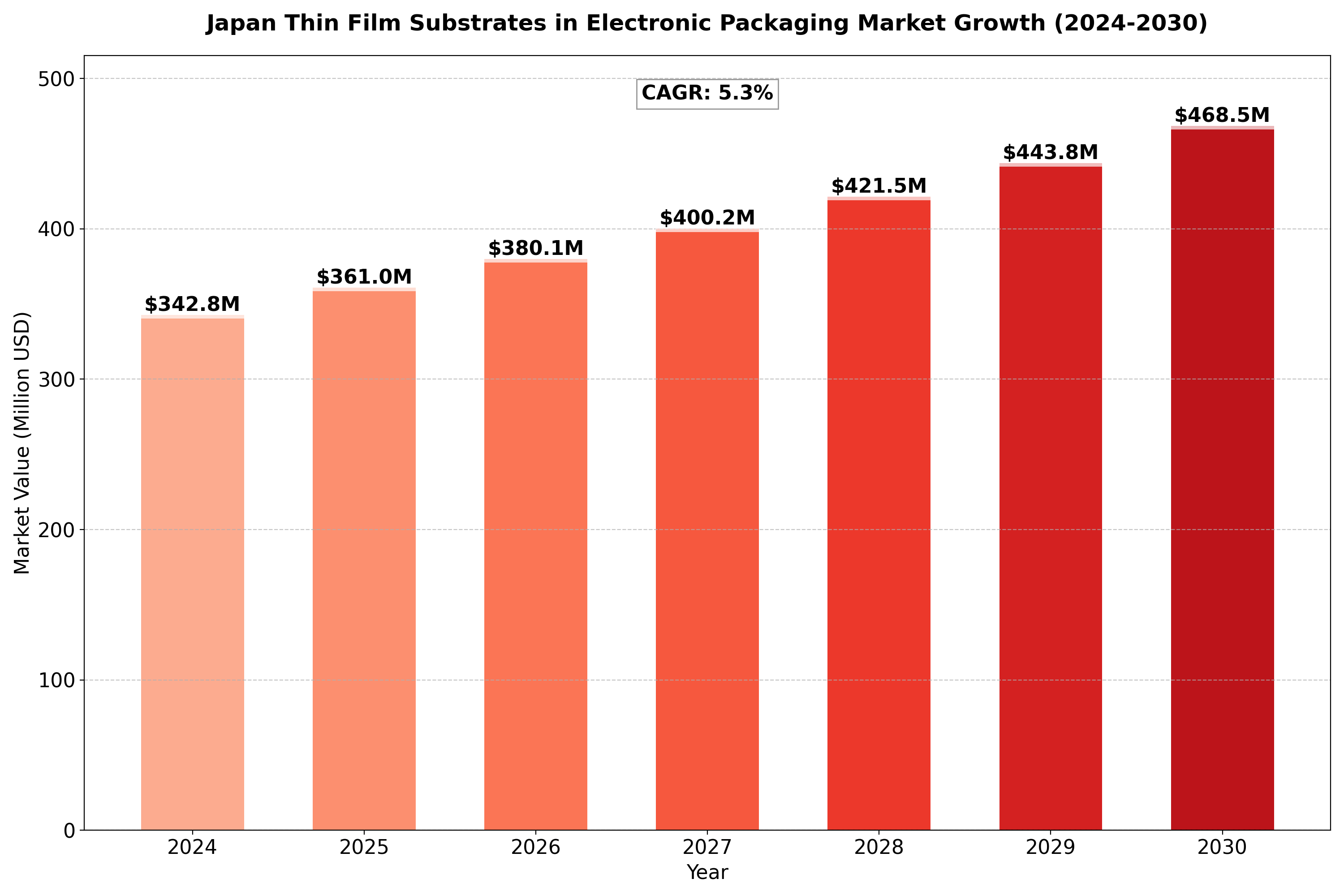
Japan Thin Film Substrates in Electronic Packaging Market size was valued at US$ 342.8 million in 2024 and is projected to reach US$ 468.5 million by 2030, at a CAGR of 5.3% during the forecast period 2024-2030.
Thin film substrates in electronic packaging are specialized platforms used for mounting and interconnecting electronic components, featuring thin film layers that enable high-density circuitry and improved electrical performance in compact electronic packages.
The Japan Thin Film Substrates in Electronic Packaging market is experiencing steady growth, driven by the increasing demand for compact and high-performance electronic devices. Key growth factors include the trend towards miniaturization in consumer electronics, the need for advanced packaging solutions in 5G and IoT devices, and the growing adoption of thin film technology in automotive electronics. Japan’s strong presence in the electronics industry and its advanced manufacturing capabilities contribute to its market position. Challenges include the complexity of integrating thin film substrates with traditional packaging technologies and the need for cost-effective production methods. Opportunities lie in developing thin film substrates for heterogeneous integration in advanced semiconductors, creating solutions for high-frequency and high-speed applications, and innovating in environmentally friendly thin film materials and processes.
This report contains market size and forecasts of Thin Film Substrates in Electronic Packaging in Japan, including the following market information:
• Japan Thin Film Substrates in Electronic Packaging Market Revenue, 2019-2024, 2024-2030, ($ millions)
• Japan Thin Film Substrates in Electronic Packaging Market Sales, 2019-2024, 2024-2030,
• Japan Top five Thin Film Substrates in Electronic Packaging companies in 2023 (%)
Report Includes
This report presents an overview of Japan market for Thin Film Substrates in Electronic Packaging , sales, revenue and price. Analyses of the Japan market trends, with historic market revenue/sales data for 2019 – 2023, estimates for 2024, and projections of CAGR through 2030.
This report focuses on the Thin Film Substrates in Electronic Packaging sales, revenue, market share and industry ranking of main manufacturers, data from 2019 to 2024. Identification of the major stakeholders in the Japan Thin Film Substrates in Electronic Packaging market, and analysis of their competitive landscape and market positioning based on recent developments and segmental revenues.
This report will help stakeholders to understand the competitive landscape and gain more insights and position their businesses and market strategies in a better way.
This report analyzes the segments data by Type, and by Sales Channels, sales, revenue, and price, from 2019 to 2030. Evaluation and forecast the market size for Humidifier sales, projected growth trends, production technology, sales channels and end-user industry.
Segment by Type
• Rigid Thin-Film Substrates
• Flexible Thin-Film Substrates
Segment by Applications
• Power Electronics
• Hybrid Microelectronics
• Multi-Chip Modules
• Others
Key Companies covered in this report:
• Shin-Etsu Chemical Co., Ltd.
• Sumitomo Chemical Co., Ltd.
• Mitsubishi Materials Corporation
• TDK Corporation
• JSR Corporation
• Nitto Denko Corporation
• Murata Manufacturing Co., Ltd.
• Fujifilm Holdings Corporation
• Panasonic Corporation
• Hitachi Chemical Co., Ltd.
Including or excluding key companies relevant to your analysis.
Competitor Analysis
The report also provides analysis of leading market participants including:
• Key companies Thin Film Substrates in Electronic Packaging revenues in Japann market, 2019-2024 (Estimated), ($ millions)
• Key companies Thin Film Substrates in Electronic Packaging revenues share in Japann market, 2023 (%)
• Key companies Thin Film Substrates in Electronic Packaging sales in Japann market, 2019-2024 (Estimated),
• Key companies Thin Film Substrates in Electronic Packaging sales share in Japann market, 2023 (%)
1. Drivers
- Growing Demand for Miniaturization in Electronics
The ongoing trend of miniaturization in electronic devices, such as smartphones, wearable devices, and high-performance computers, is driving the need for compact, efficient packaging solutions. Thin film substrates are integral to reducing the size of packaging components without compromising functionality. As Japanese electronics manufacturers emphasize cutting-edge, small-scale devices, this demand has fueled the thin film substrates market within electronic packaging. - Rise of 5G and IoT Devices
Japan is at the forefront of deploying 5G networks and IoT (Internet of Things) devices, both of which rely heavily on advanced packaging technologies for efficient signal processing and transmission. Thin film substrates, known for their high thermal and electrical performance, are essential for packaging RF modules, antennas, and sensor components in 5G and IoT devices. This increase in connected devices is driving significant growth in the thin film substrates market. - Advancements in Semiconductor Manufacturing
Japan is home to some of the most advanced semiconductor manufacturers, driving innovations in microelectronics and integrated circuits (ICs). Thin film substrates, with their superior electrical properties, play a crucial role in the packaging of high-performance semiconductor components. As semiconductor manufacturing advances in Japan to cater to artificial intelligence (AI), machine learning (ML), and edge computing applications, the demand for thin film substrates in packaging continues to rise.
2. Restraints
- High Production Costs
Thin film substrates require sophisticated manufacturing processes, including advanced materials and precision techniques. The cost of materials, such as gallium arsenide (GaAs) and silicon carbide (SiC), combined with the need for cleanroom facilities and high-end fabrication tools, leads to high production costs. For small and medium-sized enterprises (SMEs), these costs can be prohibitive, limiting their entry into the market and slowing overall growth. - Competition from Traditional Substrate Materials
While thin film substrates offer superior performance in high-frequency and miniaturized applications, they face competition from more traditional substrate materials, such as silicon and ceramic substrates. In applications where cost-effectiveness is prioritized over performance, traditional materials may be chosen, limiting the growth potential of thin film substrates in certain market segments.
3. Opportunities
- Growth in the Electric Vehicle (EV) and Autonomous Vehicle Sectors
The automotive industry in Japan is shifting towards electric vehicles (EVs) and autonomous vehicles, which depend on advanced electronics for control systems, sensors, and power modules. Thin film substrates are crucial for packaging automotive electronics, as they offer superior thermal management, which is essential for the reliability of vehicle electronics in harsh conditions. As the automotive sector continues to innovate and expand in Japan, thin film substrates will find growing opportunities in the electronic packaging for automotive applications. - Expansion of Advanced Packaging Technologies
Advanced packaging technologies, such as system-in-package (SiP) and wafer-level packaging (WLP), are becoming increasingly popular for applications requiring high-density, multi-functional components. Thin film substrates are ideal for such technologies due to their compact size and ability to handle complex circuits and multiple functionalities. The increasing adoption of advanced packaging in Japan’s semiconductor and electronics industries presents a significant growth opportunity for the thin film substrate market. - Rising Demand in Medical Electronics
Japan’s aging population is leading to an increase in demand for medical electronics, such as diagnostic devices, monitoring systems, and wearable health devices. Thin film substrates are well-suited for medical electronics packaging, where compactness, reliability, and biocompatibility are crucial. As medical device manufacturers innovate to meet growing healthcare needs, thin film substrates are expected to play a key role in the packaging of these electronic devices.
4. Challenges
- Complexity in Manufacturing Processes
The manufacturing of thin film substrates requires intricate processes, including thin film deposition, photolithography, and etching, which need precise control and specialized equipment. Ensuring consistent quality and avoiding defects during production remains a significant challenge. Even minor deviations in the production process can lead to failures in electronic components, creating hurdles for manufacturers looking to scale operations while maintaining quality. - Environmental and Regulatory Constraints
Japan has stringent environmental regulations that manufacturers must adhere to, especially when handling hazardous materials used in thin film substrates, such as arsenic compounds in GaAs substrates. Complying with these regulations adds operational costs and requires careful waste management practices. These environmental concerns, combined with the need to meet strict industry standards, can pose challenges for thin film substrate manufacturers in Japan. - Supply Chain Disruptions
Like many global industries, the electronic packaging market in Japan relies on a well-integrated supply chain for raw materials, machinery, and components. Disruptions in the supply chain, whether due to geopolitical tensions, natural disasters, or pandemics, can cause significant delays in production and distribution. Such disruptions could lead to shortages of critical materials used in thin film substrates, affecting market growth and product availability.
Key Indicators Analysed
• Market Players & Competitor Analysis: The report covers the key players of the industry including Company Profile, Product Specifications, Production Capacity/Sales, Revenue, Price and Gross Margin 2019-2030 & Sales with a thorough analysis of the market’s competitive landscape and detailed information on vendors and comprehensive details of factors that will challenge the growth of major market vendors.
• Japann Market Analysis: The report includes Japann market status and outlook 2019-2030. Further the report provides break down details about each region & countries covered in the report. Identifying its sales, sales volume & revenue forecast. With detailed analysis by types and applications.
• Market Trends: Market key trends which include Increased Competition and Continuous Innovations.
• Opportunities and Drivers: Identifying the Growing Demands and New Technology
• Porters Five Force Analysis: The report provides with the state of competition in industry depending on five basic forces: threat of new entrants, bargaining power of suppliers, bargaining power of buyers, threat of substitute products or services, and existing industry rivalry.
Key Benefits of This Market Research:
• Industry drivers, restraints, and opportunities covered in the study
• Neutral perspective on the market performance
• Recent industry trends and developments
• Competitive landscape & strategies of key players
• Potential & niche segments and regions exhibiting promising growth covered
• Historical, current, and projected market size, in terms of value
• In-depth analysis of the Thin Film Substrates in Electronic Packaging Market
• Overview of the regional outlook of the Thin Film Substrates in Electronic Packaging Market
Key Reasons to Buy this Report:
• Access to date statistics compiled by our researchers. These provide you with historical and forecast data, which is analyzed to tell you why your market is set to change
• This enables you to anticipate market changes to remain ahead of your competitors
• You will be able to copy data from the Excel spreadsheet straight into your marketing plans, business presentations or other strategic documents
• The concise analysis, clear graph, and table format will enable you to pinpoint the information you require quickly
• Provision of market value (USD Billion) data for each segment and sub-segment
• Indicates the region and segment that is expected to witness the fastest growth as well as to dominate the market
• Analysis by geography highlighting the consumption of the product/service in the region as well as indicating the factors that are affecting the market within each region
• Competitive landscape which incorporates the market ranking of the major players, along with new service/product launches, partnerships, business expansions, and acquisitions in the past five years of companies profiled
• Extensive company profiles comprising of company overview, company insights, product benchmarking, and SWOT analysis for the major market players
• The current as well as the future market outlook of the industry concerning recent developments which involve growth opportunities and drivers as well as challenges and restraints of both emerging as well as developed regions
• Includes in-depth analysis of the market from various perspectives through Porter’s five forces analysis
• Provides insight into the market through Value Chain
• Market dynamics scenario, along with growth opportunities of the market in the years to come
• 6-month post-sales analyst support
We offer additional regional and global reports that are similar:
• Global Thin Film Substrates in Electronic Packaging Market
• United States Thin Film Substrates in Electronic Packaging Market
• Japan Thin Film Substrates in Electronic Packaging Market
• Germany Thin Film Substrates in Electronic Packaging Market
• South Korea Thin Film Substrates in Electronic Packaging Market
• Indonesia Thin Film Substrates in Electronic Packaging Market
• Brazil Thin Film Substrates in Electronic Packaging Market
Customization of the Report: In case of any queries or customization requirements, please connect with our sales team, who will ensure that your requirements are meet.

Get Sample Report PDF for Exclusive Insights
Report Sample Includes
- Table of Contents
- List of Tables & Figures
- Charts, Research Methodology, and more...


