Japan AI-Grade Photoresist Market Insights
Global Japan AI-Grade Photoresist market size was valued at USD 0.45 billion in 2025. The market will increase from USD 0.48 billion in 2026 to USD 0.78 billion by 2034, exhibiting a CAGR of 5.1% during the forecast period.
AI‑grade photoresist is a chemically engineered coating applied during semiconductor lithography that enables sub‑10 nm patterning through superior resolution, line‑edge roughness control and defect mitigation achieved via machine‑learning‑optimized formulations.
The sector gains momentum because semiconductor manufacturers are investing heavily in advanced node production and rising demand for high‑performance computing fuels adoption of EUV lithography platforms that rely on AI‑grade resist chemistries, while firms pursue higher yield rates.
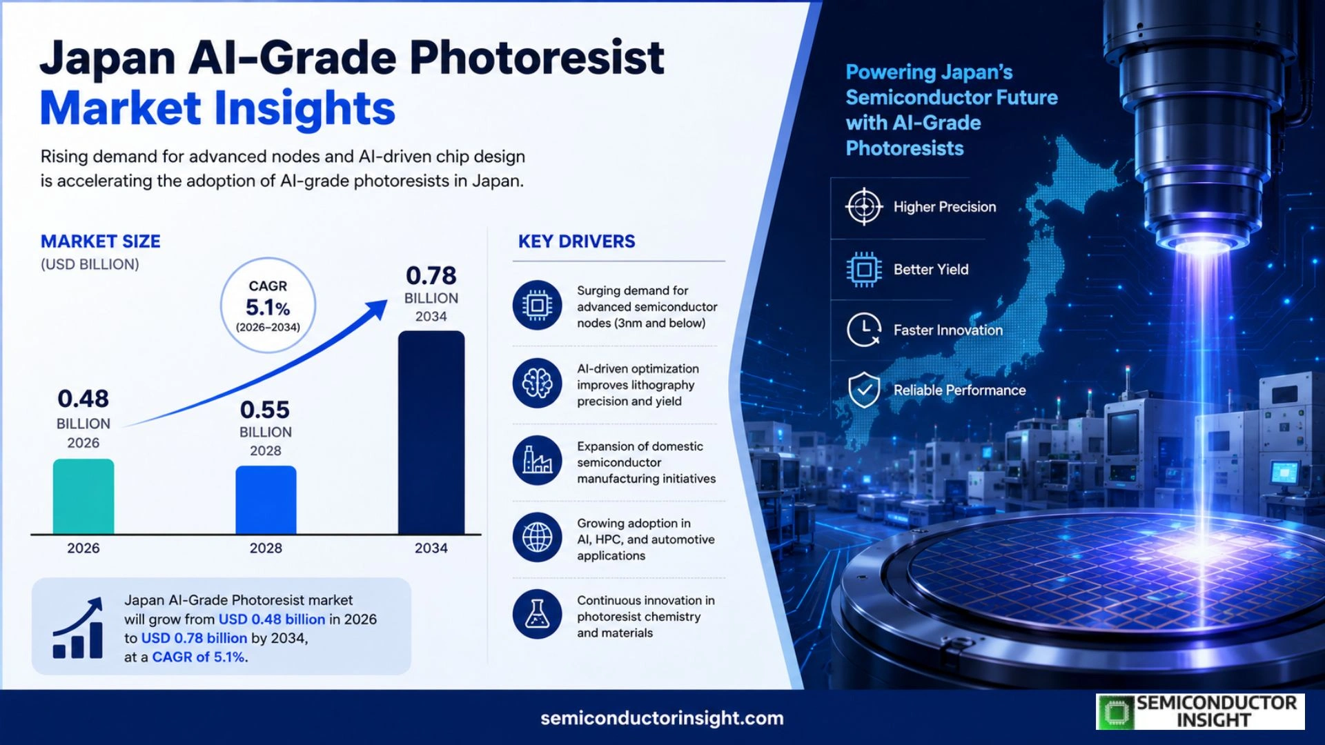
MARKET DRIVERS
Advanced Lithography Demands
The push for sub‑10 nm patterning in logic and memory devices forces manufacturers to seek photoresists that can deliver finer resolution without compromising line‑edge roughness. AI‑enhanced formulation algorithms enable molecular designs that meet these specifications, giving Japan AI-Grade Photoresist Market a clear technical advantage over conventional chemistries.
Government‑Backed R&D Incentives
National programs aimed at strengthening semiconductor self‑sufficiency allocate sizable subsidies to projects that integrate artificial‑intelligence tools into material development. This fiscal support lowers the effective cost of adoption for domestic fabs, encouraging early‑stage pilots that rapidly generate performance data.
➤ “AI‑driven formulation reduces defect density by roughly one third, shaving weeks off the qualification cycle.”
For suppliers, the convergence of high‑resolution requirements and policy incentives translates into a need to build analytics platforms and up‑skill formulation teams, reshaping their go‑to‑market strategies across Japan AI-Grade Photoresist Market.
MARKET CHALLENGES
Capital Intensity of New Processes
Introducing AI‑grade photoresists demands upgrades to coating tracks, bake ovens, and metrology suites. The upfront outlay often exceeds the budget thresholds of mid‑size fab operators, leading many to defer migration until a clear ROI is demonstrated on a pilot line.
Other Challenges
Talent Gap
The intersection of polymer chemistry and machine‑learning expertise is scarce in Japan. Companies must either invest heavily in internal training or partner with academic labs, both of which extend project timelines and increase overhead.
MARKET RESTRAINTS
Supply‑Chain Bottlenecks
High‑purity precursor chemicals required for AI‑optimized photoresists are produced by a limited number of overseas facilities. Disruptions in these pipelines can delay batch scaling, forcing fab planners to maintain safety stocks of legacy materials.
In addition, the stringent qualification protocols enforced by leading semiconductor manufacturers extend the time needed to certify a new resist, slowing market penetration despite evident performance benefits.
MARKET OPPORTUNITIES
Quantum‑Era Device Manufacturing
Emerging quantum‑computing chips require ultra‑low‑defect photoresists to pattern delicate qubit structures. AI‑grade formulations, capable of predictive defect mitigation, are uniquely positioned to satisfy these exacting specifications, opening a niche but high‑value revenue stream.
Beyond domestic demand, neighboring Asian economies are beginning to explore AI‑assisted lithography solutions. Exporting expertise and material licenses can unlock additional growth avenues for Japanese suppliers.
Strategic alliances between traditional chemical firms and AI start‑ups are expected to accelerate co‑development cycles, creating differentiated product portfolios that can capture market share from legacy providers.
Japan AI-Grade Photoresist Market Trends
Advanced Node Adoption Fuels Resist Innovation
Japan AI-Grade Photoresist Market is being reshaped by semiconductor manufacturers’ shift toward sub‑10 nm nodes. AI‑grade formulations, engineered through machine‑learning algorithms, deliver tighter line‑edge roughness and lower defectivity, which directly translates into higher wafer yields on EUV platforms. As Japanese fabs ramp up production for high‑performance computing chips, the demand for resist materials that can sustain the stringent overlay tolerances of advanced logic devices rises sharply. This pressure creates an incentive for resist suppliers to embed AI capabilities into their product pipelines, shortening development cycles and enabling rapid formulation tweaks in response to lithography tool feedback.
Other Trends
R&D Investment and Talent Scarcity
Companies operating in Japan AI-Grade Photoresist Market are allocating a larger share of operating budgets to research that merges photochemistry with data‑driven modeling. The scarcity of chemists who also understand deep‑learning frameworks forces firms to partner with local universities and to sponsor graduate programs focused on computational materials science. Such collaborations accelerate prototype validation and reduce time‑to‑market for next‑generation resist chemistries, while also creating a pipeline of specialists who can navigate both laboratory and algorithmic environments.
Strategic Alliances with Lithography Equipment Vendors
Another observable shift is the deepening of joint‑development agreements between resist producers and EUV equipment manufacturers. By synchronizing the chemical profile of AI‑grade resists with the illumination and mask‑error‑correction capabilities of the latest scanners, partners achieve more predictable process windows. For end‑users, this translates into fewer mask reworks and lower total cost of ownership. The collaborative model also encourages shared intellectual property, allowing both parties to protect innovations while still delivering a cohesive solution to the fab floor.
COMPETITIVE LANDSCAPE
Key Industry Players
Competitive Dynamics in Japan’s AI‑Grade Photoresist Segment
Tokyo Ohka Kogyo (TOK) anchors the Japanese market, leveraging its deep lithography heritage and extensive R&D pipeline to supply AI‑optimized resists to major fabs. Its partnership network with equipment vendors and chipmakers creates a feedback loop that accelerates formulation tweaks based on real‑time production data. JSR Corporation follows closely, differentiating through a portfolio that blends high‑resolution chemistry with environmentally conscious solvents, a combination that appeals to manufacturers seeking yield improvements without expanding waste treatment capacity. Both firms benefit from a supply chain that is largely domestic, reducing lead‑time volatility and enabling rapid iteration on machine‑learning‑driven resin blends. The concentration of these two players has spurred a modest consolidation trend, where smaller specialty firms are either absorbed or become dedicated subcontractors to the market leaders.
Beyond the dominant pair, a constellation of niche contributors shapes the competitive fringe. Fujifilm leverages its imaging expertise to tailor photo‑patterning agents that excel in defect suppression, while Toray Industries applies its polymer know‑how to enhance line‑edge roughness control. Shin‑Etsu Chemical and Sumitomo Chemical supply high‑purity precursors that underpin the performance of AI‑grade formulations, positioning themselves as critical upstream enablers. Hitachi High‑Technologies and HOYA Corporation offer complementary metrology and mask‑making services that reinforce the value chain. International entrants such as DuPont Japan and Merck KGaA Japan maintain a foothold through joint development agreements, ensuring that the Japanese market remains receptive to global innovation while preserving local manufacturing depth.
List of Key Photoresist Companies Profiled
- Tokyo Ohka Kogyo
- Tokyo Ohka Kogyo
- JSR Corporation
- JSR Corporation
- Fujifilm Holdings
- Fujifilm Holdings
- Toray Industries
- Toray Industries
- Shin‑Etsu Chemical
- Sumitomo Chemical
- Hitachi High‑Technologies
- HOYA Corporation
- DuPont Japan
- Merck KGaA Japan
Segment Analysis:
| Segment Category | Sub-Segments | Key Insights |
| By Type |
|
Organic AI-Grade Photoresist
|
| By Application |
|
Logic Devices
|
| By End User |
|
Integrated Device Manufacturers
|
| By Technology |
|
Machine‑Learning Formulation Optimization
|
| By Market Driver |
|
Advanced Node Production
|
Regional Analysis: Japan AI-Grade Photoresist Market
Asia‑Pacific
The relentless push toward sub‑3 nm nodes compels manufacturers to adopt photoresists with superior etch resistance and nanoscale uniformity. Japan’s aggressive roadmap for high‑volume production fuels demand for materials that can tolerate higher exposure doses without compromising yield.
Tightening emissions standards in Japan have prompted vendors to develop low‑VOC formulations. Compliance pathways are now intertwined with performance metrics, pressuring suppliers to innovate under regulatory constraints.
Integration of AI‑driven process control tools in fab environments accelerates feedback on resist performance, enabling rapid formulation tweaks that align with real‑time lithography data.
Established Japanese chemical houses are consolidating niche players to broaden their product portfolios, while new entrants leverage proprietary nanocomposite technologies to carve out specialty segments.
North America
In the United States, the Japan AI‑Grade Photoresist Market is viewed through the lens of cross‑border R&D collaborations. American fabless firms increasingly source Japanese‑designed resists for prototype runs, attracted by the material’s precision under extreme ultraviolet (EUV) exposure. Venture capital inflows into AI‑enhanced lithography software are feeding a feedback loop that pressures Japanese suppliers to align their roadmaps with North American design standards. Meanwhile, trade policies shape pricing dynamics, prompting manufacturers to adopt flexible supply contracts that mitigate tariff volatility.
Europe
European semiconductor clusters, notably in the Netherlands and Germany, treat Japanese photoresist technology as a strategic complement to their own process innovations. Collaborative projects under the European Horizon framework often benchmark Japanese formulations against local alternatives, emphasizing defect suppression in high‑volume manufacturing. Sustainability expectations in the EU drive demand for resists that balance performance with reduced environmental impact, nudging Japanese producers to prioritize green chemistry without sacrificing line‑edge accuracy.
South America
South American markets remain peripheral yet increasingly curious about the Japan AI‑Grade Photoresist Market as regional governments pursue semiconductor fabs to diversify their industrial base. Brazil’s emerging pilot lines rely on imported Japanese resists for initial trials, appreciating the material’s stability under varied climate conditions. Supply-chain considerations, such as longer lead times and currency fluctuations, encourage local distributors to maintain strategic inventories, ensuring uninterrupted access for niche manufacturing outfits.
Middle East & Africa
The Middle East’s investment in downstream semiconductor assembly makes the Japan AI‑Grade Photoresist Market an attractive sourcing option for high‑precision lithography steps. United Arab Emirates’ smart‑manufacturing initiatives cite Japanese resin performance as a benchmark for quality. In Africa, nascent research parks are experimenting with Japanese photoresist blends to support academic fab projects, seeing the technology as a catalyst for skill development and future industrial participation.
Report Scope
This market research report provides a comprehensive analysis of the Japan AI-Grade Photoresist Market , covering the forecast period 2026–2034. It offers detailed insights into market dynamics, technological advancements, competitive landscape, and key trends shaping the industry.
Key focus areas of the report include:
- Market Overview: The report begins with an overview outlining its current market scenario, key growth indicators, and industry transformation drivers. It discusses macroeconomic factors, demand–supply balance, regulatory landscape, and the strategic role of semiconductors in powering advancements across industries such as automotive, telecommunications, consumer electronics, and industrial automation.
- Market Size & Forecast: Historical data and future projections for revenue, unit shipments, and market value across major regions and segments.
- Segmentation Analysis: Detailed breakdown by product type, technology, application, and end-user industry to identify high-growth segments and investment opportunities.
- Regional Insights: Insights into market performance across North America, Europe, Asia-Pacific, Latin America, and the Middle East & Africa, including country-level analysis where relevant.
- Competitive Landscape: Profiles of leading market participants, including their product offerings, R&D focus, manufacturing capacity, pricing strategies, and recent developments such as mergers, acquisitions, and partnerships.
- Technology Trends & Innovation: Assessment of emerging technologies, integration of AI/IoT, semiconductor design trends, fabrication techniques, and evolving industry standards.
- Market Drivers & Restraints: Evaluation of factors driving market growth along with challenges, supply chain constraints, regulatory issues, and market-entry barriers.
- Stakeholder Insights: Insights for component suppliers, OEMs, system integrators, investors, and policymakers regarding the evolving ecosystem and strategic opportunities.
Primary and secondary research methods are employed, including interviews with industry experts, data from verified sources, and real-time market intelligence to ensure the accuracy and reliability of the insights presented.
FREQUENTLY ASKED QUESTIONS:
What is the current market size of Japan AI-Grade Photoresist Market?
-> Japan AI-Grade Photoresist market size will increase from USD 0.48 billion in 2026 to USD 0.78 billion by 2034, exhibiting a CAGR of 5.1%.
Which key companies operate in Japan AI-Grade Photoresist Market?
-> Key players include Axalta Coating Systems, AkzoNobel, BASF SE, PPG, Sherwin-Williams, and 3M, among others.
What are the key growth drivers?
-> Key growth drivers include railway infrastructure investments, urbanization, and demand for durable coatings.
Which region dominates the market?
-> Asia-Pacific is the fastest-growing region, while Europe remains a dominant market.
What are the emerging trends?
-> Emerging trends include bio-based coatings, smart coatings, and sustainable rail solutions.

Get Sample Report PDF for Exclusive Insights
Report Sample Includes
- Table of Contents
- List of Tables & Figures
- Charts, Research Methodology, and more...
 Download Sample Report PDF