MARKET INSIGHTS
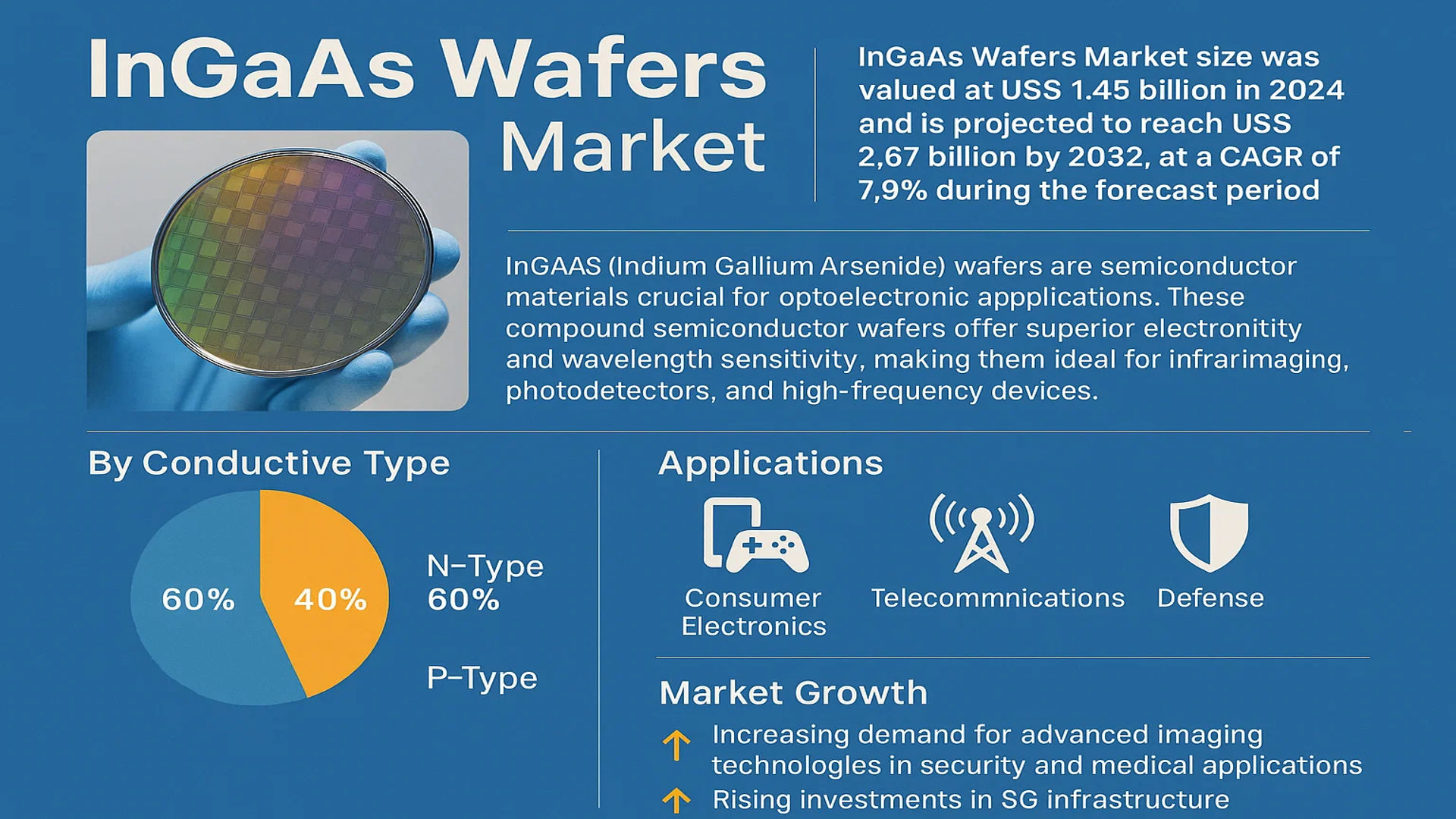
The global InGaAs Wafers Market size was valued at US$ 1.45 billion in 2024 and is projected to reach US$ 2.67 billion by 2032, at a CAGR of 7.9% during the forecast period 2025-2032.
InGaAs (Indium Gallium Arsenide) wafers are semiconductor materials crucial for optoelectronic applications. These compound semiconductor wafers offer superior electron mobility and wavelength sensitivity, making them ideal for infrared imaging, photodetectors, and high-frequency devices. The market is segmented by conductive type into N-type and P-type wafers, with varying applications across consumer electronics, telecommunications, and defense sectors.
The market growth is driven by increasing demand for advanced imaging technologies in security and medical applications, coupled with rising investments in 5G infrastructure. While the semiconductor industry faced a slowdown in 2022 with global growth at 4.4%, the optoelectronics segment maintained strong performance. Key players like Coherent Corp and VIGO Photonics are expanding production capacities to meet growing demand for infrared sensors and communication devices, particularly in North America and Asia-Pacific markets.
MARKET DYNAMICS
MARKET DRIVERS
Expansion of Infrared Imaging Applications Fuels InGaAs Wafer Demand
The global InGaAs wafer market is experiencing robust growth primarily driven by increasing adoption in infrared imaging applications. With superior sensitivity to wavelengths between 900-1700 nm, InGaAs wafers have become critical components in night vision systems, surveillance equipment, and industrial inspection tools. The defense sector alone accounted for over 35% of infrared detector applications in 2023, with expanding budgets for modernized military technologies accelerating market demand. Furthermore, the semiconductor industry’s shift toward compound semiconductor materials continues opening new opportunities, as InGaAs offers higher electron mobility compared to traditional silicon.
Telecommunications Infrastructure Upgrades Create Sustained Market Growth
The transition to 5G networks and fiber optic communication systems is significantly boosting the InGaAs wafer market. These wafers serve as essential substrates for photodetectors in optical communication networks, which require high-speed, low-noise performance. Network operators worldwide invested over $200 billion in fiber deployment in 2023, with projections indicating continued infrastructure expansion throughout this decade. As data transmission speeds exceed 100 Gbps in next-gen networks, the superior performance characteristics of InGaAs-based components become increasingly critical, driving sustained market expansion.
Scientific Research and Space Applications Create Niche Growth Opportunities
Increasing government and private investment in space exploration and scientific instrumentation provides additional momentum for InGaAs wafer adoption. Advanced spectroscopy systems, astronomical sensors, and Earth observation satellites increasingly utilize InGaAs detectors for their superior near-infrared response. The global space economy, valued at over $450 billion in 2023, continues expanding with nearly 2000 active satellites now requiring sophisticated sensing capabilities. These high-value applications create premium market segments where superior performance justifies higher production costs, pushing manufacturers to develop more advanced wafer solutions.
MARKET RESTRAINTS
High Production Costs and Limited Yield Rates Constrain Market Penetration
Despite strong demand, the InGaAs wafer market faces significant constraints from complex manufacturing processes that result in relatively low yield rates. The epitaxial growth techniques required for high-quality InGaAs layers remain technically challenging, with defect densities significantly higher than conventional silicon wafers. Production costs can be up to 20 times that of equivalent silicon solutions, making adoption difficult in price-sensitive applications. This cost barrier limits market expansion into consumer electronics and other high-volume sectors, confining wafers primarily to specialized applications where their performance advantages can justify premium pricing.
Other Restraints
Supply Chain Vulnerabilities
Reliance on rare earth materials and geopolitical factors affecting indium supply create periodic market instability. With over 70% of indium production concentrated in specific geographic regions, trade restrictions or production disruptions can severely impact wafer manufacturing capacity and pricing stability.
Alternative Technology Competition
Emerging silicon-based technologies offering improved infrared sensitivity challenge InGaAs dominance in certain applications. As silicon photonics and quantum dot technologies mature, they threaten to capture mid-range performance segments where cost considerations outweigh the slight performance advantages of III-V materials.
MARKET CHALLENGES
Technical Complexity in Large Diameter Wafer Development
The industry faces significant technical hurdles in scaling InGaAs wafer production to larger diameters critical for manufacturing efficiency. While silicon wafers have transitioned to 300mm standards, most InGaAs production remains limited to 100-150mm sizes due to fundamental material properties. This size limitation prevents full integration with mainstream semiconductor fabrication lines, requiring specialized handling and processing that increases overall system costs. Thermal expansion mismatch and defect propagation during crystal growth remain primary obstacles, with industry yield rates for larger wafers still below commercial viability thresholds in most cases.
Other Challenges
Standardization Gaps
The lack of industry-wide standards for InGaAs wafer specifications creates uncertainties for both suppliers and end-users. Variation in crystal orientation, doping profiles, and surface preparation methods between manufacturers complicates the design-in process for component producers, slowing adoption cycles and increasing qualification costs.
Workforce Specialization Requirements
The specialized knowledge required for III-V semiconductor processing creates workforce bottlenecks. With fewer than 10 major academic programs worldwide focusing on compound semiconductor manufacturing, the industry faces severe talent shortages that constrain production scaling efforts.
MARKET OPPORTUNITIES
Emerging Quantum Technology Applications Open New Frontiers
The rapidly developing quantum technology sector presents transformative opportunities for InGaAs wafer suppliers. Quantum communication systems, quantum computing photonic interconnects, and single-photon detectors all require the unique properties offered by InGaAs materials. Government investments in quantum research exceeded $3 billion globally in 2023, with projections indicating compound annual growth rates above 30% through 2030. This creates a premium application space where wafer suppliers can command higher margins while driving fundamental material innovations that may eventually benefit broader commercial markets.
Automotive LiDAR Expansion Creates High-Growth Potential
The autonomous vehicle revolution is driving substantial demand for advanced sensing solutions where InGaAs detectors offer strategic advantages. LiDAR systems for automotive applications increasingly adopt InGaAs-based receivers for their superior performance in eye-safe 1550nm wavelengths. With over 30 automotive OEMs now developing autonomous platforms and sensor suites, this application space could account for nearly 15% of InGaAs wafer demand by 2027. The industry’s stringent reliability requirements and willingness to adopt advanced materials create favorable conditions for wafer suppliers to establish long-term partnerships with automotive electronics providers.
Medical Imaging Innovations Drive New Application Development
The healthcare sector’s increasing adoption of advanced imaging modalities creates additional avenues for InGaAs wafer deployment. Optical coherence tomography systems, minimally invasive surgical tools, and next-generation diagnostic imaging platforms all benefit from InGaAs-based detectors. With global medical imaging equipment markets projected to exceed $50 billion by 2026, these applications offer wafer suppliers stable, long-term growth potential. The stringent regulatory environment in medical device manufacturing also creates competitive moats for established suppliers with proven quality systems and regulatory compliance expertise.
InGaAs WAFERS MARKET TRENDS
Rising Demand for High-Performance Photodetectors Drives Market Growth
The InGaAs (Indium Gallium Arsenide) wafers market is witnessing significant growth due to the increasing demand for advanced photodetectors in telecommunications, spectroscopy, and imaging applications. The global market was valued at approximately $143 million in 2024 and is expected to grow at a CAGR of 7.5% through 2032. This growth is attributed to the exceptional optoelectronic properties of InGaAs, which enables superior performance in near-infrared (NIR) and short-wave infrared (SWIR) sensing. Additionally, industries requiring high-speed data transmission, such as fiber-optic communications, are intensifying the adoption of InGaAs-based components, significantly influencing market expansion.
Other Trends
Expansion in Semiconductor Laser Applications
The surge in demand for semiconductor lasers in medical, defense, and industrial applications is fueling the uptake of InGaAs wafers. These wafers provide high electron mobility and an ideal bandgap for efficient laser diode performance. With the global semiconductor laser market projected to surpass $16 billion by 2027, the adoption of InGaAs wafers is accelerating, particularly in laser-based sensing and optical communication systems. Furthermore, advancements in laser diode efficiency and miniaturization are opening new opportunities in portable and IoT-enabled devices, reinforcing market demand.
Growing Adoption in Solar Energy and Optical Sensing
InGaAs wafers are increasingly being utilized in solar energy applications due to their ability to enhance photovoltaic efficiency in multi-junction solar cells. The push toward renewable energy solutions has elevated R&D efforts, with governments and private entities investing in next-generation solar technologies. Meanwhile, in optical sensing, InGaAs-based detectors are gaining traction in autonomous vehicles, industrial automation, and medical diagnostics, owing to their superior sensitivity in SWIR imaging. As industries continue to prioritize precision and energy efficiency, the market is poised to experience sustained growth driven by these high-value applications.
COMPETITIVE LANDSCAPE
Key Industry Players
Innovation and Expansion Drive Competition in the InGaAs Wafer Market
The global InGaAs wafers market features a dynamic competitive landscape with both established semiconductor players and specialized manufacturers vying for market share. Coherent Corp has emerged as a dominant force, leveraging its expertise in photonics and materials science to capture significant market share. The company’s acquisition of II-VI Incorporated in 2022 strengthened its position in compound semiconductor technologies including InGaAs production.
VIGO Photonics SA and Sensors Unlimited (now part of Collins Aerospace) have maintained strong positions in the market through their focus on high-performance infrared detection applications. These companies have benefited from increasing defense and aerospace applications where InGaAs detectors offer superior sensitivity in the short-wave infrared spectrum.
Market competition is intensifying as companies expand their production capabilities and develop advanced wafer technologies. Several players are investing in larger diameter wafer production (up to 6-inch) to meet the growing demand from consumer electronics and telecommunications sectors. While established players dominate in traditional sectors like defense, emerging applications in LiDAR and optical communications are creating opportunities for specialized suppliers.
Meanwhile, regional competition is shaping the market dynamics significantly. Asian manufacturers like XIAMEN POWERWAY are gaining traction through cost-competitive offerings, challenging North American and European suppliers on price in certain market segments.
List of Key InGaAs Wafer Companies Profiled
- UniversityWafer, Inc. (U.S.)
- VIGO Photonics SA (Poland)
- Sensors Unlimited (United Technologies) (U.S.)
- Coherent Corp (U.S.)
- Codex International (U.K.)
- Princeton Infrared Technologies (U.S.)
- Anritsu Company Inc. (Japan)
- XIAMEN POWERWAY (China)
Recent market developments show a trend toward vertical integration, with several companies expanding capabilities across the entire value chain from wafer production to detector fabrication. This strategic positioning helps manufacturers maintain quality control while optimizing costs – a critical factor as prices face downward pressure in commercial applications.
Segment Analysis:
By Type
Conductive Type N Wafers Hold Majority Share Owing to Superior Optoelectronic Properties
The market is segmented based on type into:
- Conductive Type N
- Subtypes: Standard and customized doping levels
- Conductive Type P
- Subtypes: Standard and customized doping levels
By Application
Photodetector Segment Accounts for Largest Application Due to Increasing Demand in Industrial and Defense Applications
The market is segmented based on application into:
- Consumer Electronics Products
- Photodetector
- Sub-segments: Short-wave infrared (SWIR) imaging, fiber optic communications
- Semiconductor Laser
- Solar Battery
- Others
By End User
Semiconductor Industry Represents Leading End-User Segment Fueled by Miniaturization Trends
The market is segmented based on end user into:
- Semiconductor Industry
- Telecommunication Sector
- Renewable Energy Providers
- Research Laboratories
- Others
Regional Analysis: InGaAs Wafers Market
Asia-Pacific
The Asia-Pacific region dominates the global InGaAs wafers market due to strong semiconductor manufacturing ecosystems in China, Japan, and South Korea. China’s drive toward technological self-sufficiency and Japan’s leadership in precision semiconductor materials contribute significantly to regional demand. The photodetector application segment is particularly strong due to growing adoption in telecommunications and industrial sensing. While Japan maintains technological supremacy in wafer production, China’s aggressive investments in domestic fabrication facilities (expected to reach $150 billion by 2025) are reshaping supply chains. South Korea’s display and memory chip manufacturers are increasingly adopting InGaAs wafers for next-generation optoelectronic applications.
North America
North America demonstrates robust demand for high-performance InGaAs wafers, particularly in defense and aerospace applications. The U.S. accounts for over 60% of regional consumption, driven by advanced R&D in quantum computing and infrared imaging technologies. Major defense contractors and national laboratories maintain steady demand for specialized wafer formulations. Canada’s emerging photonics clusters in Ontario and Quebec are creating new growth opportunities, while Mexico serves primarily as a manufacturing partner for U.S. firms. The region benefits from strong intellectual property protections and collaborative research initiatives between industry and academia.
Europe
Europe’s market shows balanced growth across industrial and scientific applications, with Germany and France leading adoption. The region’s strength lies in high-value niche applications, including medical imaging and environmental monitoring systems. EU-funded projects like the Photonics21 initiative foster innovation in wafer-based technologies. Strict material purity standards and emphasis on sustainable semiconductor manufacturing processes differentiate European applications. While production volumes trail Asia, European firms command premium pricing for specialty wafers used in scientific instrumentation and precision measurement devices.
South America
The region remains a developing market for InGaAs wafers, with Brazil accounting for most industrial demand in oil/gas sensing and agricultural monitoring applications. Limited local manufacturing capacity creates reliance on imports, primarily from U.S. and Asian suppliers. Recent economic stabilization in key markets is facilitating gradual adoption in academic research institutions. Argentina shows particular promise in optical communication applications, though currency volatility and infrastructure limitations constrain faster market expansion.
Middle East & Africa
Market growth centers on Israel’s advanced tech sector and Gulf nations’ smart city initiatives. Israel’s strong defense electronics industry drives specialized wafer demand, while UAE investments in semiconductor testing facilities create new application opportunities. South Africa’s mining sector utilizes InGaAs-based sensors for mineral exploration. The region shows increasing engagement with global supply chains, though limited local expertise and high import costs remain barriers to widespread adoption outside niche applications.
Report Scope
This market research report provides a comprehensive analysis of the Global and regional InGaAs Wafers market, covering the forecast period 2025–2032. It offers detailed insights into market dynamics, technological advancements, competitive landscape, and key trends shaping the industry.
Key focus areas of the report include:
- Market Size & Forecast: Historical data and future projections for revenue, unit shipments, and market value across major regions and segments. The Global InGaAs Wafers market was valued at US$ 1.45 billion in 2024 and is projected to reach US$ 2.67 billion by 2032.
- Segmentation Analysis: Detailed breakdown by product type (Conductive Type N, Conductive Type P), application (Consumer Electronics, Photodetectors, Semiconductor Lasers, Solar Batteries), and end-user industries.
- Regional Outlook: Insights into market performance across North America, Europe, Asia-Pacific, Latin America, and the Middle East & Africa, with Asia-Pacific currently holding the largest market share.
- Competitive Landscape: Profiles of leading market participants including UniversityWafer, Inc., VIGO Photonics SA, Sensors Unlimited, and Coherent Corp, covering their product offerings and strategic developments.
- Technology Trends & Innovation: Assessment of emerging semiconductor fabrication techniques and material science advancements in InGaAs wafer production.
- Market Drivers & Restraints: Evaluation of factors such as growing demand for infrared sensors and photodetectors versus challenges in raw material availability and high production costs.
- Stakeholder Analysis: Strategic insights for semiconductor manufacturers, OEMs, and investors regarding the evolving InGaAs wafer ecosystem.
The research employs both primary and secondary methodologies, including interviews with industry experts and analysis of verified market data, to ensure accurate and reliable insights.
FREQUENTLY ASKED QUESTIONS:
What is the current market size of Global InGaAs Wafers Market?
-> InGaAs Wafers Market size was valued at US$ 1.45 billion in 2024 and is projected to reach US$ 2.67 billion by 2032, at a CAGR of 7.9% during the forecast period 2025-2032.
Which key companies operate in Global InGaAs Wafers Market?
-> Key players include UniversityWafer, Inc., VIGO Photonics SA, Sensors Unlimited, Coherent Corp, and Princeton Infrared Technologies, among others.
What are the key growth drivers?
-> Key growth drivers include increasing demand for infrared imaging, expansion of fiber optic communication networks, and adoption in defense and aerospace applications.
Which region dominates the market?
-> Asia-Pacific currently holds the largest market share, driven by semiconductor manufacturing growth in China, Japan, and South Korea.
What are the emerging trends?
-> Emerging trends include advancements in wafer fabrication techniques, development of larger diameter wafers, and integration with III-V compound semiconductors.

Get Sample Report PDF for Exclusive Insights
Report Sample Includes
- Table of Contents
- List of Tables & Figures
- Charts, Research Methodology, and more...
 Download Sample Report PDF