Key Statistics
Key Takeaways
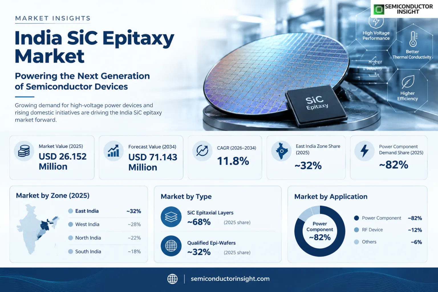
- Market value: The Indian epitaxial silicon carbide value chain represents USD 26.152 million in 2025, with a projected USD 71.143 million by 2034 at 11.8% annual growth. The commercial product is a grown crystalline semiconductor layer or epi-wafer supplied for Indian device activity, not the value of an uncoated substrate or a completed transistor.
- Epitaxial thickness mix: Films classified as below 12 µm represent a modeled ~68% of the 2025 market, while the above-30 µm category accounts for ~32%. High-voltage structures can require more demanding thick-layer processes, but those specialist requirements must not be mistaken for evidence that all Indian wafer customers already purchase commercial thick epitaxy.
- Application demand: Power-component processing leads with an estimated ~82% share in 2025, compared with ~12% for RF devices and ~6% for other research-oriented applications. Wafer acceptance depends on thickness control, doping uniformity, defect density and device-specific electrical performance; generic crystal procurement figures are not a substitute for epitaxial revenue.
- Indian geography: East India contributes a modeled ~32% of market value because Odisha has an unusually visible epitaxy investment pipeline. West India holds ~24%, South India ~22%, North India ~15%, and Central and Northeast India ~7%; these shares reflect demand and project exposure rather than a census of operating commercial reactors.
- Industrial qualification: Coherent documents commercial SiC epitaxial material and AIXTRON supplies deposition equipment; the latter is an equipment vendor, not a merchant epi-wafer producer. RIR Power Electronics installed epitaxy reactors in Odisha in September 2026, but regulatory steps still separated the installation milestone from commercial output at the announcement date.
India SiC Epitaxy Market Overview
India SiC epitaxy market was valued at USD 26.152 million in 2025 and is projected to reach USD 71.143 million by 2034, expanding at a 11.8% CAGR. The East India zone represents an estimated ~32% of 2025 Indian value, with power-component uses comprising ~82% of demand. The addressable product includes SiC epitaxial layers and qualified epi-wafers for Indian customers, with both imported material and legitimate domestic development activity within scope.
Silicon carbide epitaxy deposits a precisely controlled semiconductor crystal layer on a compatible wafer, giving device engineers control over electrical properties that a polished bare crystal cannot provide alone. Power MOSFETs and diodes rely on epitaxial thickness, background defects and intentional doping to meet blocking-voltage and reliability targets. The Indian market therefore involves deposition services and epi-wafer material supply for semiconductor development, including early qualification lots. It does not automatically include the capital cost of reactors or the downstream sales value of packaged power modules.
The market boundary follows epitaxial growth and the delivered SiC epi-wafer where the Indian purchaser uses that product in a device or research programme. A bare SiC substrate without deposited layers belongs to a different upstream materials category, even though it becomes the foundation of epitaxial processing. Similarly, a fabricated transistor includes lithography, implantation, contacts and testing that are not epitaxial sales. Imported epi-wafers, engineering samples and Indian pilot-stage growth activity can contribute to the defined market, while unbuilt factory capacity does not count as delivered commercial production.
Indian policy is expanding the potential customer pipeline through SiC semiconductor projects in Odisha and broader power-device investment. The planned SiCSem fabrication facility creates a future requirement for epitaxial material, while RIR Power Electronics has disclosed a phased Bhubaneswar programme involving epitaxy equipment. Installation of a reactor is an important engineering milestone because utilities, process gases and cleanroom readiness must be established before qualification. Nevertheless, a machine standing in a facility cannot demonstrate a stable wafer output, device yield or a confirmed order book without further operating evidence.
International suppliers illustrate the technical direction without establishing Indian sales by themselves. Coherent announced 200 mm SiC epitaxial wafer availability in September 2024 and later disclosed thick-layer capability for high-voltage devices in April 2026. AIXTRON announced its hundredth G10-SiC reactor shipment in September 2025, supporting global growth in epitaxial manufacturing equipment. Those developments matter to India because local engineers can benchmark uniformity, throughput and wafer size, but they should not be converted directly into Indian production figures or domestic revenue.
The 2025 model allocates Indian value across five domestic zones and two publisher-defined thickness categories. The categories below 12 µm and above 30 µm are retained as published; the unclassified intermediate interval is not presented as a separately measured segment. Thin layers lead in the modeled current mix, while thick growth has stronger prospective momentum from multi-kilovolt power conversion. Supplier competitiveness rests on usable epi area, defect screening, doping repeatability, customer device qualification and the ability to scale beyond demonstration batches without compromising reliability.
Segment Analysis: By Type
Epitaxial thickness influences voltage design, deposition duration and yield exposure. The publisher identifies a below-12 µm category with ~68% modeled 2025 share and an above-30 µm category with ~32%; no additional intermediate class is separately quantified. The thinner class is associated with more established power-device processes, while thick epitaxy serves demanding high-voltage structures and specialised qualification, making the two product categories commercially distinct despite their common SiC chemistry.
| Epitaxial thickness | Technical and commercial demand | Modeled position |
|---|---|---|
| Thickness below 12 µm | This group covers thin SiC epitaxial layers used in qualifying relatively established switching devices and development wafers. Process engineers review layer thickness, doping concentration, surface morphology and defects introduced during growth. Uniformity over a 150 mm wafer may matter more to a buyer than a nominal thickness figure, because small local deviations can change electrical behaviour after subsequent processing. The market is linked to repeatable device manufacturing rather than simply the sale of an uncoated crystal wafer. | The below-12 µm category leads at ~68% of 2025 modeled revenue and expands at ~10.7% annually in the model. A larger installed base of conventional device structures supports the starting allocation, while reactor recipe development and competition from integrated wafer suppliers influence pricing. Customers require documented growth conditions, traceable lots and evidence that the same film properties can be reproduced over successive batches. |
| Thickness above 30 µm | Thicker epitaxial structures are relevant where power devices must sustain higher blocking voltages, often requiring extended growth cycles and particularly careful defect control. The supplier has to manage doping profiles, surface roughness, crystal quality and cost over more deposited material. Coherent disclosed thick SiC epitaxy platforms for device architectures up to 10 kV in April 2026, an international capability benchmark rather than proof of Indian commercial volumes. Qualification is application-specific and can involve several device-design iterations. | The above-30 µm category carries an estimated ~32% starting share and a faster modeled ~13.8% annual expansion through 2034. Its growth case depends on high-voltage industrial systems, grid infrastructure and specialty research. A high potential growth rate does not remove the risk that a thick epi-wafer may be rejected after expensive processing if defect density or electrical uniformity misses the customer specification. |
Thin epitaxy and established device programmes
Below 12 µm layers can be suitable for certain power-semiconductor designs in which customers prioritise reproducible electrical parameters over extreme voltage capability. A wafer purchaser may first qualify a small run, inspect the surface for triangular defects or step bunching, and then fabricate electrical test structures. Acceptance typically depends on the combined behaviour of substrate and grown layer rather than on the deposition recipe alone. Indian engineering teams benefit when material suppliers provide measurement reports that can be compared between pilot batches and eventual production lots.
Commercial adoption of thin epitaxy depends on matching a wafer format to the available process line. A reactor qualified for 150 mm substrates may not produce the same radial uniformity on 200 mm material without a new recipe and hardware evaluation. The Indian category is therefore assessed through delivered epi-wafer value and development services rather than inferred from overseas equipment shipment counts. Local service providers can compete by shortening turnaround for measurement, sample analysis and customer-specific growth adjustments.
Thick epitaxy and high-voltage qualification
Growth above 30 µm can increase deposition time and expose the process to more opportunities for defect propagation, which makes reliable throughput an important commercial variable. High-voltage MOSFETs and diodes may need tightly controlled doping across a thick drift region to achieve their electrical targets. Coherent’s April 2026 announcement highlights the direction of international thick-epitaxy engineering, but Indian market uptake still depends on customer prototypes, fabrication partnerships and repeat orders. A technology demonstration is not automatically equivalent to qualified high-volume production.
For Indian buyers, the most attractive supplier is not necessarily the one advertising the thickest deposited film. Uniformity, wafer bow after growth, electrical breakdown distribution and failure-analysis support determine whether the epi-wafer can proceed to later process steps. The modeled faster expansion of thick layers reflects increasing interest in rail, industrial and power-distribution applications. Projected demand remains conditional on semiconductor device programmes advancing from laboratory evaluation to repeatable manufacturing.
Segment Analysis: By Application
Power-component applications represent ~82% of 2025 Indian epitaxial demand in the model because wide-bandgap devices are primarily evaluated for efficient high-voltage switching. RF devices represent ~12%, and other uses ~6%. The application split concerns epitaxial wafer and deposition value, not the revenue of a charging station, radio system or inverter containing the finished semiconductor. Customers specify the layer characteristics required by the device architecture and its reliability target.
| Application | Demand characteristics |
|---|---|
| Power Component | At ~82% modeled share, power-device applications dominate demand for SiC epi-wafers used in MOSFETs, Schottky diodes and related high-efficiency switching structures. Industrial drives, renewable conversion, EV charging and power distribution motivate the downstream engineering. Material orders arise earlier in the chain, when fabs specify thickness, doping and allowable defects for device production. The modeled ~12.2% application growth is conditional on project commissioning, qualification yields and customers accepting repeatable batches rather than simply approving capital expenditure. |
| RF Device | RF applications account for ~12% of modeled 2025 value and have a projected ~10.4% growth profile. High-frequency device designs can use different epitaxial stacks, material resistivity and electrical testing from vertical power switches. Domestic RF procurement may involve telecom, research and defence engineering partners with low-volume specialist needs. These customers may prioritise signal integrity and thermal performance over wafer throughput, and their requirements should not be inferred from the total national mobile infrastructure budget. |
| Others | Other applications represent ~6% of the base-year model and include experimental structures, material-characterisation runs and unusual semiconductor research requirements. Such purchases may involve a limited number of epi-wafers with unusually strict specifications, creating revenue disproportionate to wafer count. This segment is sensitive to university grants, industrial pilot projects and specialist supplier availability. The category is not a residual for unrelated GaN or silicon deposition, which are excluded from the defined SiC market. |
A power-device customer can require a low-defect drift layer, while an RF customer may demand a distinct combination of material properties and device geometry. The same epitaxy reactor platform does not guarantee that both customers will accept the same process recipe. Indian suppliers and international partners must therefore organise qualifications by device class, voltage or frequency requirement, wafer diameter and downstream fabrication process. The power-led mix favours firms capable of tracing epitaxial measurements to device performance rather than merely advertising deposition throughput.
Early orders can be irregular because a failed electrical test may send a development team back to the epitaxial specification. A single engineering customer may request 2 or 3 thickness variants before settling on a preferred process window. That iterative activity belongs to the market when a qualifying epi-wafer or deposition service is delivered, but it cannot be extrapolated into the volume of a proposed future fab. This distinction protects the commercial interpretation of Indian investment announcements.
Regional Analysis
Five domestic zones capture the location of Indian customer activity, engineering influence and planned epitaxial processing rather than five independent merchant-wafer factories. East India leads at ~32% of modeled 2025 value because Odisha has identifiable reactor and device-fab initiatives. West India follows at ~24%, South India at ~22%, North India at ~15%, and Central and Northeast India at ~7%; growth differs with customer qualification and project commissioning.
How is Indian SiC epitaxy demand distributed across domestic zones?
The five-zone allocation separates existing technical customers from announced capacity that still requires process and commercial qualification. Odisha’s reactor installation provides a more specific epitaxy signal than a generic electronics investment, while western and southern zones have broader industrial and design demand. North India contributes downstream semiconductor links and laboratories; central and northeastern locations represent smaller research and supply-chain opportunities. Regional revenue follows the Indian customer’s material or service purchase, not the registered office of a global supplier.
Projected growth rates differ because zones begin from different combinations of research, procurement and plant-development activity. East India has the strongest modeled trajectory at ~13.5% annually, compared with ~10.8% for West India and ~11.7% for South India. The shares and growth rates are modeled allocations of one national market, not official state revenue releases. A change in the timing of Odisha qualification could shift the realised pattern without changing the technical necessity of SiC epitaxial layers.
| Region | Position | Growth outlook | Demand profile | What decides supplier selection |
|---|---|---|---|---|
| East India | ~32% modeled 2025 share | ~13.5% CAGR to 2034 | USD 8.369m base value and USD 26.159m modeled endpoint | Odisha reactor readiness and customer device qualification |
| West India | ~24% modeled 2025 share | ~10.8% CAGR to 2034 | USD 6.276m base value and USD 15.797m modeled endpoint | Industrial design procurement and imported epi-wafer availability |
| South India | ~22% modeled 2025 share | ~11.7% CAGR to 2034 | USD 5.753m base value and USD 15.574m modeled endpoint | Design-led specification and automotive reliability qualification |
| North India | ~15% modeled 2025 share | ~10.1% CAGR to 2034 | USD 3.923m base value and USD 9.326m modeled endpoint | Device test ecosystems and downstream semiconductor partners |
| Central & Northeast India | ~7% modeled 2025 share | ~9.9% CAGR to 2034 | USD 1.831m base value and USD 4.287m modeled endpoint | Specialist distribution and institutional development budgets |
Competitive Landscape and Commercial Epitaxy Capabilities
India’s SiC epitaxy competitive field combines international epi-wafer suppliers, domestic project developers and process-equipment companies with different commercial roles. Coherent markets SiC epitaxial materials directly; AIXTRON manufactures the growth reactors that customers use. RIR is advancing Indian epitaxy capability but its September 2026 installation announcement did not yet confirm commercial production. These distinctions prevent equipment shipments, proposed device-fab capacity and bare-substrate sales from being counted as merchant epitaxial wafer revenue.
Epi-wafer suppliers compete through uniformity, controllable doping, thickness options, surface morphology and predictable defect density. Coherent offers a documented materials portfolio spanning SiC substrates and epitaxy, with announcements concerning 200 mm material and thick-layer high-voltage capability. Such product depth can help Indian device teams specify wafers for laboratory work and eventual manufacturing. A vendor’s global technical portfolio is relevant to qualification, but its corporate revenue cannot be directly treated as Indian SiC epitaxy market sales.
Deposition equipment manufacturers influence the market through throughput, wafer-size compatibility and recipe support, yet their reactor invoices belong to capital equipment rather than epitaxial wafer supply. AIXTRON’s G10-SiC platform is designed for multiwafer deposition, and the company reported a hundredth system shipment in September 2025. Indian operators considering equipment investments need to evaluate gas handling, utility requirements, process transfer and customer acceptance. Installing the equipment does not automatically establish a qualified product line or recurring wafer sales.
RIR Power Electronics represents an important domestic development case because its Bhubaneswar plan explicitly includes SiC epitaxial wafer manufacturing. September 2026 reporting described completed reactor installation and infrastructure readiness, with remaining statutory requirements before commercial operation. That distinction is material to supplier classification: RIR is a potential domestic producer under qualification, not a proven volume epi-wafer vendor on the basis of installation alone. Its progress could change local sourcing patterns once customers validate output.
Other Indian semiconductor initiatives are best classified by their specific activities. The SiCSem project concerns compound-semiconductor fabrication, and CDIL’s Mohali milestone relates to downstream power-device manufacturing and packaging. Both can generate demand for qualified epitaxial layers but do not independently establish merchant epi-wafer capacity. Competitive positioning will depend on transparent role definitions, reliable wafer traceability and service support across the full device qualification cycle.
Tier structure
| Tier | Companies | Basis of competition |
|---|---|---|
| Direct epitaxial material suppliers | Coherent and qualified international SiC epi-wafer producers | Direct competition centres on delivered crystalline layer specifications, defect inspection, wafer diameter, lot-to-lot consistency and customer acceptance. A global capability statement establishes product availability but not the amount shipped to India. Supplier rankings should therefore distinguish documented technical portfolios from unverified Indian revenue claims. |
| Domestic development participants | RIR Power Electronics and emerging India SiC project teams | India’s development tier includes reactor installation, process commissioning, wafer evaluation and potential future local supply. RIR’s September 2026 milestone is meaningful because equipment was installed, while statutory clearance and commercial production were still separate. Announced plans are not equivalent to completed customer deliveries or verified operating capacity. |
| Equipment and downstream ecosystem | AIXTRON; SiCSem; CDIL; Infineon Technologies | AIXTRON supplies epitaxial deposition systems; SiCSem has a planned device-fabrication role; CDIL packages power semiconductors; Infineon develops power devices. These organisations shape the market’s technical and demand environment without all being merchant SiC epi-wafer vendors. Their activity must be described by function rather than combined into an unsupported supplier-share ranking. |
Key companies profiled
- Coherent Corp.
- AIXTRON SE
- RIR Power Electronics Limited
- Infineon Technologies AG
- Wolfspeed, Inc.
- SiCSem Private Limited
- Continental Device India Limited (CDIL)
Production Process, Qualification and India Capacity Pipeline
SiC epitaxy transforms a polished compatible crystal wafer into a device-ready semiconductor layer through carefully controlled deposition. Reactor loading, gas flows, temperature, dopant incorporation and surface preparation determine whether the resulting film satisfies a customer’s specification. India’s pipeline includes imported epi-wafer products and planned local process capability, but the installed reactor count and announced fabrication targets cannot substitute for measured, saleable epi-wafer output.
A typical production sequence begins with substrate cleaning and inspection, proceeds through high-temperature epitaxial growth, and ends with thickness mapping, doping assessment and defect screening. Wafer diameter and target layer thickness influence deposition time and the number of wafers processed per batch. Device customers often require trial wafers before releasing a production specification, so a supplier may generate development revenue while full-volume commercial qualification is still underway. The quality of the grown layer is judged through subsequent electrical test structures as well as surface metrology.
The distinction between bare material and epitaxial value is central to India’s supply chain. A bare 4H-SiC wafer can be imported, coated with an epitaxial layer in India, and later sent to a device fab for implantation and metallisation. Only the relevant epitaxial product or processing value belongs in this market. Reactor capital expenditure, packaging and finished transistor sales remain separate. This approach avoids adding the full value of the same physical wafer at every successive production stage.
International manufacturing is advancing toward larger wafer formats, including Coherent’s 200 mm epi-wafer capability and AIXTRON’s equipment designed for 150 mm and 200 mm production. India’s current demand may still include smaller engineering lots and imported qualified materials. Domestic reactor installation is therefore an opportunity to build process expertise rather than a guarantee of immediate competitiveness at global high-volume yield levels. Customers will assess repeatability, downtime, lot certification and supplier responsiveness before changing established material sources.
Market Dynamics: Drivers, Restraints and Growth Opportunities
India’s SiC epitaxy market moves from USD 26.152 million in 2025 toward USD 71.143 million by 2034 at a 11.8% CAGR. Domestic power-device programmes, high-voltage layer requirements and supplier process learning create the principal growth forces. Commissioning risk, technical defects and specialised equipment costs counterbalance these opportunities. The impact framework assigns distinct contributions to factors affecting the epitaxial layer and epi-wafer market, rather than transferring downstream inverter or semiconductor equipment revenue into the material forecast.
MARKET DRIVERS
Drivers Impact Analysis*
| Market Drivers | Impact Rank | CAGR Contribution (%) | 2026–2028 | 2029–2031 | 2032–2034 |
|---|---|---|---|---|---|
| Indian SiC device fabrication and qualification | High | +5.80% | High | High | Medium |
| High-voltage industrial power semiconductor demand | High | +4.20% | Medium | High | High |
| Epitaxy process localisation and supply resilience | Medium-High | +3.20% | Medium | High | High |
| Thick-layer SiC material engineering | Medium | +2.40% | Medium | Medium | High |
| Others (research demand and RF qualification) | Low | +1.10% | Medium | Low | Low |
Device projects create recurring layer specifications
Approved and developing Indian compound-semiconductor facilities can become long-term customers for qualified SiC epitaxial material. The commercial sequence is gradual: sample growth, electrical characterisation, customer device trials, process adjustments and then repeat orders. Odisha’s identified project pipeline provides a geographic focal point, but approvals alone do not establish sales. Suppliers able to document consistent film properties and support device engineers across multiple trial cycles are better positioned to convert project activity into sustained material revenue.
Higher-voltage systems require tailored drift layers
Industrial power distribution, rail systems, renewable conversion and datacentre infrastructure can require devices designed for challenging electrical environments. A thick, well-controlled SiC epitaxial layer can support high blocking voltages, provided doping and defect specifications are met. Coherent’s April 2026 thick-epitaxy disclosure provides an international technical reference. Indian adoption will depend on device programmes reaching qualification milestones and on material suppliers proving repeatability rather than relying on theoretical voltage capability alone.
Domestic processing may shorten qualification loops
Locally accessible epitaxy engineering can reduce the time between a failed device test and a revised deposition recipe. RIR’s reactor installation creates a potential foundation for such process work once remaining approvals and technical validation are completed. The value proposition includes metrology, technical communication and small-batch flexibility, not only wafer throughput. Indian customers may still import substrates and specialised epi-wafers where established overseas processes offer better quality or delivery assurance.
Thick epitaxy adds differentiated service value
The modeled above-30 µm category grows more rapidly than thin layers because high-voltage structures can require more material, longer growth cycles and tighter process control. These demands raise the value of engineering support and reproducible deposition. The opportunity is constrained by the risk of defects over extended growth, making qualification economics central. Suppliers with credible process data can compete on technical reliability rather than treating all epi-wafers as interchangeable commodity sheets.
MARKET RESTRAINTS
Restraints Impact Analysis*
| Market Restraints | Impact Rank | CAGR Contribution (%) | 2026–2028 | 2029–2031 | 2032–2034 |
|---|---|---|---|---|---|
| Defect sensitivity and customer qualification delays | High | -1.80% | High | High | Medium |
| Capital and operating costs for epitaxial reactors | Medium-High | -1.30% | High | Medium | Medium |
| Imported materials and process dependence | Medium | -0.90% | High | Medium | Low |
| Others (regulatory and commissioning timing) | Low | -0.90% | High | Medium | Low |
Crystal and growth defects reduce usable output
Dislocations, surface pits, step bunching and doping nonuniformity can make an epi-wafer unsuitable for its intended device even when the deposition process appears complete. The loss is commercially significant because later semiconductor steps add cost before a failure is discovered. Customers therefore require inspection maps, test structures and traceable batch data. New Indian processes may need several qualification rounds before a reliable yield profile is established.
Reactor economics require stable utilisation
Epitaxial deposition uses specialised high-temperature reactors, process gases, monitoring systems and trained operators. A new facility may be technically capable of growing a layer yet struggle to recover costs if orders remain small or irregular. AIXTRON’s global equipment shipment milestone demonstrates the existence of mature industrial platforms, not the profitability of every local installation. Indian operators must match capacity to customer schedules and avoid treating announced investment as immediate wafer sales.
Imported supply and process transfer remain relevant
Domestic programmes may depend on foreign substrates, proven epi-wafer suppliers and international process expertise while local manufacturing matures. Switching material source can trigger renewed device reliability tests, making customers cautious about rapid procurement changes. The result is a transition period in which imported and Indian development material coexist. Market growth can proceed without complete domestic self-sufficiency, but supply continuity and traceability remain essential commercial constraints.
MARKET OPPORTUNITIES
Qualification services near emerging SiC projects
An Indian specialist can create value through epitaxial layer inspection, recipe optimisation, wafer mapping and failure analysis even before operating a high-volume growth facility. Device teams often need repeated experiments to identify acceptable doping and defect windows. Offering rapid engineering feedback and documented results can shorten procurement decisions and build long-term relationships. The opportunity is especially relevant to Odisha project development and southern semiconductor design networks.
High-voltage layer customisation for industrial customers
Power systems designed for elevated voltage can require epitaxial thickness and doping combinations outside standard catalogue grades. Suppliers that can tailor growth conditions and demonstrate electrical repeatability may secure higher-value niche orders. The thick-layer market is not automatically large in unit volume, but each accepted wafer can carry substantial technical content. Partnerships between materials specialists and Indian device developers can accelerate the conversion of laboratory specifications into production-ready products.
Coordinated substrate-to-epi sourcing arrangements
Customers can simplify technical responsibility by coordinating bare-wafer selection, epitaxial growth and downstream device testing across qualified partners. Such arrangements require clarity about which party supplies the substrate and who is responsible for growth defects or process changes. They can reduce rejected lots and improve schedule predictability for Indian semiconductor programmes. The market opportunity lies in delivering a qualified epitaxial product, without counting the same bare substrate or finished device as additional epi revenue.
Value Chain and Routes to Indian Customers
The epitaxy supply chain links SiC crystal suppliers, wafer finishing, epitaxial deposition, electrical metrology, device fabrication and power-electronics system integration. A commercial epi-wafer order can be supplied from overseas or processed in India when capability and qualification permit. Buyers must agree on wafer diameter, layer thickness, doping profile, defect limits, packaging and traceability before the material can be accepted for semiconductor production.
Substrate selection and surface preparation. The initial crystal wafer affects the quality ceiling of the grown layer. Dislocations and surface damage can propagate during deposition, while wafer bow may complicate uniform thermal processing. Buyers must specify crystal orientation, surface preparation and defect limits before evaluating epitaxial performance. An integrated supplier can coordinate these steps, but the market value of a bare wafer and a deposited layer should remain commercially distinguishable where they are separately supplied.
Process control and acceptance. Epitaxy providers manage temperature profiles, precursor chemistry, gas flow and growth duration to meet customer layer requirements. Acceptance testing may include thickness maps, doping uniformity, surface defects and electrical measurements from processed test structures. A single successful wafer is insufficient to demonstrate a stable manufacturing line; repeat batches and statistically meaningful yield information matter. Indian project teams should therefore establish process control plans before committing to long-term material procurement.
Domestic engineering and imported material. India can participate in SiC epitaxy through design specifications, metrology, process trials and eventual local growth while continuing to import proven epi-wafers. RIR’s Odisha reactor installation provides a specific pathway for domestic processing, subject to remaining approvals and qualification. Coherent’s international products provide a separate route for customers seeking established material capability. These approaches can coexist, and the national market should reflect delivered epitaxial value rather than a binary import-versus-domestic classification.
Customer contracts and technical support. A successful supply agreement needs more than a price per wafer. Customers may require agreed thickness tolerance, doping range, defect map format, replacement procedures and notice of recipe changes. For research customers, responsive engineering support can be particularly valuable because device specifications evolve during development. For industrial customers, consistency across lots and documented failure analysis can determine whether a supplier progresses from samples to repeat production deliveries.
Recent Developments in SiC Epitaxy and India Semiconductor Capacity
- 16 September 2026 India reactor installation
RIR Power Electronics reported installation of silicon carbide epitaxial wafer manufacturing reactors and supporting utilities at its Bhubaneswar facility. The installation advances domestic technical readiness, but the company indicated that remaining statutory and regulatory requirements preceded commercial production. This event is evidence of a developing Indian processing capability, not an announcement of completed merchant epi-wafer shipments or a measured national output figure. Source - 9 April 2026 Direct global thick epitaxy
Coherent announced advances in thick silicon carbide epitaxy supporting power-device designs up to 10 kV, using 150 mm and 200 mm platforms. The capability illustrates how advanced layer control can serve high-voltage industrial and datacentre applications. Its global technical significance is relevant to Indian product development, but the announcement does not identify a quantity of Indian epi-wafer shipments or verify domestic thick-layer production. Source - 22 September 2025 Global equipment milestone
AIXTRON announced shipment of its hundredth G10-SiC epitaxy system, with the milestone unit destined for a European power-device manufacturer. The platform supports industrial multiwafer SiC layer growth and demonstrates the scale of global deposition-equipment adoption. Equipment shipment is distinct from sale of an epitaxial wafer, so this milestone informs manufacturing capability and technology direction rather than being booked as Indian material revenue. Source - 15 August 2025 Adjacent India fab approval
Indian government documentation described the SiCSem compound-semiconductor project in Odisha and its planned wafer fabrication and packaging activities. A fabrication investment can support future demand for SiC epitaxial layers, but approved production targets do not establish operating epi-wafer growth or confirmed merchant material sales. The relevant market implication is a developing customer and qualification pipeline whose conversion depends on commissioning and repeatable semiconductor processing. Source - 7 August 2025 Domestic project support
RIR Power Electronics disclosed Odisha fiscal support for its Bhubaneswar silicon carbide semiconductor programme. The funding milestone supported a phased manufacturing initiative that included plans for epitaxy and high-power devices. Project support can improve the outlook for local material qualification, yet the announcement should not be treated as evidence that a commercial epitaxial wafer line had already completed commissioning or generated ongoing customer shipments. Source - 26 September 2024 Direct global epi-wafer supply
Coherent announced expansion of silicon carbide epitaxial wafer production, including 200 mm material capability and commercial shipments. The disclosure documents a direct supplier’s progress toward larger-diameter epitaxy and improved materials availability for semiconductor manufacturers. For India, it serves as evidence of accessible international technology and supply options, not a declaration of Indian domestic 200 mm wafer growth or a standalone national market-size anchor. Source - 23 April 2024 Adjacent process equipment
AIXTRON disclosed that Vishay selected its SiC multiwafer batch deposition technology for a European semiconductor facility. The event shows continued investment in epitaxy process equipment and reinforces the importance of uniform growth for power-device manufacturing. It is an equipment procurement milestone outside India, so the relevant lesson concerns reactor qualification and global capacity trends rather than direct Indian epitaxial material sales. Source
REPORT SCOPE & SEGMENTATION
| Attribute | Details |
|---|---|
| Market | India SiC Epitaxy |
| Base year | 2025 |
| Estimate year | 2026 |
| Forecast year | 2034 |
| Currency | USD million |
| Revenue boundary | Silicon carbide epitaxial layers, epi-wafers and qualifying deposition services supplied to India, including legitimate development-stage activity; excludes uncoated bare substrates, finished devices, reactor sales and unrelated GaN or silicon processes. |
| By Type | Thickness below 12 µm · Thickness above 30 µm |
| By Application | Power Component · RF Device · Others |
| By Region | Single-country market split into five domestic Indian zones; zone shares represent modeled demand and project exposure, not separate reported state revenue or five operating epitaxy facilities. East IndiaOdisha · West Bengal · emerging SiC epitaxy processing and eastern technical procurement West IndiaGujarat · Maharashtra · industrial power engineering and material sourcing South IndiaKarnataka · Tamil Nadu · semiconductor design and mobility electronics North IndiaPunjab · Uttar Pradesh · downstream power devices and research laboratories Central & Northeast IndiaMadhya Pradesh · Assam · institutional engineering and developing electronics |
| Key Companies Profiled | Coherent Corp.; AIXTRON SE; RIR Power Electronics; Infineon Technologies; Wolfspeed; SiCSem; Continental Device India |
| Customization Scope | Domestic-zone demand, thin and thick SiC epitaxial structures, wafer-diameter compatibility, growth uniformity, dopant control, defect mapping, reactor commissioning milestones, and customer qualification pathways. |
Frequently Asked Questions
How large is the India SiC epitaxy market?
The market is valued at USD 26.152 million in 2025 and projected to reach USD 71.143 million in 2034, implying 11.8% compound annual growth. This series concerns epitaxial semiconductor layers, epi-wafer material and related growth value supplied to Indian customers. It excludes the value of uncoated SiC crystal substrates when sold separately, as well as complete transistors, power modules and equipment capital expenditure.
Which Indian zone has the largest modeled share?
East India leads with ~32% of 2025 modeled value because Odisha has identifiable SiC epitaxy reactor installations and a broader semiconductor project pipeline. West India follows at ~24%, South India at ~22%, North India at ~15%, and Central and Northeast India at ~7%. The allocation describes Indian demand and development exposure; it does not assert that commercial epitaxial wafer output has begun in every zone.
What thickness category leads Indian SiC epitaxy demand?
Layers below 12 µm represent an estimated ~68% of 2025 value, compared with ~32% for layers above 30 µm. The two categories reproduce the publisher-defined type segmentation; no independent intermediate class is claimed. Thicker growth can serve higher-voltage designs but often needs longer deposition cycles and tighter defect management, which helps explain its modeled faster expansion through 2034.
Which application accounts for the most demand?
Power components dominate at an estimated ~82% of 2025 value, with RF devices at ~12% and other uses at ~6%. Power-device customers evaluate epitaxial layers for MOSFETs, diodes and related switching structures. The market counts qualified layer or epi-wafer transactions rather than revenue from complete electric vehicles, industrial drives, renewable installations or communication infrastructure that may eventually use those devices.
Has RIR started commercial SiC epitaxy production in Odisha?
RIR disclosed reactor installation and infrastructure readiness at Bhubaneswar in September 2026, but the announcement also stated that commercial production remained dependent on outstanding statutory and regulatory formalities. The milestone therefore establishes equipment progress, not confirmed merchant wafer sales. Commercial status should be reassessed using later operating disclosures, qualified wafer shipments and customer acceptance rather than assuming installation equals production.
How is SiC epitaxy different from a bare substrate?
A bare silicon carbide wafer supplies the crystalline foundation, whereas epitaxy adds a controlled semiconductor layer with specified thickness and electrical properties. A device manufacturer may buy a bare wafer, procure deposition as a service, or purchase an integrated epi-wafer. This market follows the epitaxial component of that value chain and excludes unrelated wafer finishing, semiconductor packaging and the full selling price of finished power devices.
Why do high-voltage devices need thick epitaxy?
Blocking voltage requirements can influence the thickness and doping of the SiC drift layer, making thicker epitaxial structures relevant to demanding industrial power systems. Coherent disclosed 150 mm and 200 mm thick-layer capability for device designs up to 10 kV in April 2026. Such global technical progress provides a reference point, but Indian sales depend on actual device programmes, material qualification and repeatable wafer yield.
What determines the price and acceptance of an epi-wafer?
Customers consider substrate quality, deposition thickness, doping uniformity, surface defects, wafer diameter and the amount of usable device area. Longer growth times and demanding electrical specifications can raise costs, while poor yield can eliminate any advantage from a lower quoted wafer price. Supplier qualification usually involves sample batches, metrology reports and device-level tests before a production order is accepted.
Are AIXTRON reactor shipments counted as SiC epitaxy revenue?
No. AIXTRON sells epitaxial deposition equipment, which enables customers to manufacture semiconductor layers but is a different commercial product from a delivered SiC epi-wafer. Its September 2025 hundredth G10-SiC shipment is useful evidence of global process-equipment adoption. The Indian epitaxy materials market counts the relevant grown-layer product or service, not the entire reactor purchase price.
How do imports and domestic development coexist?
Indian semiconductor projects can import established SiC epi-wafers while domestic organisations develop growth processes, testing capabilities and eventual production capacity. Imported material may remain necessary for demanding applications even after local pilot activity begins. The market includes legitimate Indian purchases and qualifying development transactions without requiring complete national self-sufficiency, while excluding planned factory capacity that has not yet resulted in a delivered product or service.
Research Sources & Evidence Base
Get Sample Report PDF for Exclusive Insights
Report Sample Includes
- Table of Contents
- List of Tables & Figures
- Charts, Research Methodology, and more...
 Download Sample Report PDF