
India AI Semiconductor Fabless Design Market Insights
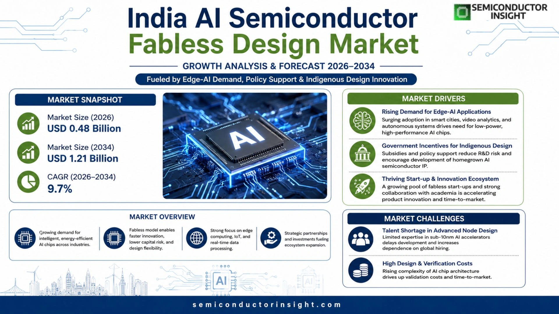
Global India AI semiconductor fabless design market size was valued at USD 0.42 billion in 2025. The market is projected to grow from USD 0.48 billion in 2026 to USD 1.21 billion by 2034, exhibiting a CAGR of 9.7% during the forecast period.
AI semiconductor fabless design refers to the practice of creating advanced artificial‑intelligence‑optimized integrated circuits without owning manufacturing facilities; designers focus on architecture, verification, and IP development while partnering with foundries for production.
Key activities include developing neural‑network accelerators, low‑power inference engines, and custom ASICs tailored for edge‑AI workloads.
The sector’s momentum stems from heightened government support under India’s National Strategy on Artificial Intelligence, escalating venture capital inflows into home‑grown chip startups, and rising demand for localized AI solutions across automotive, healthcare, and IoT domains.
Collaborations between Indian design firms such as Saankhya Labs and Ineda Systems with global foundries accelerate time‑to‑market. Furthermore, strategic initiatives by multinational players establishing R&D hubs in Bengaluru reinforce ecosystem depth and signal sustained investment opportunities.
MARKET DRIVERS
Rising Demand for Edge‑AI Applications
The proliferation of video analytics, smart‑city sensors, and autonomous‑vehicle prototypes in Indian metros is compelling system integrators to source low‑power, high‑performance AI chips. Because fabless firms can iterate designs faster than traditional foundries, they are increasingly preferred for time‑critical deployments.
Government Incentives for Indigenous Design
Recent policy announcements earmark subsidies for design houses that localize AI semiconductor IP. This financial cushion reduces R&D risk and encourages start‑ups to pursue bespoke architectures rather than import legacy solutions.
➤ Design agility combined with policy support creates a feedback loop that accelerates the entry of niche AI chips into the Indian ecosystem.
Overall, the convergence of application‑driven demand and targeted fiscal measures is reshaping the competitive landscape of India AI Semiconductor Fabless Design Market, prompting both domestic players and foreign investors to reassess their go‑to‑market strategies.
MARKET CHALLENGES
Talent Shortage in Advanced Node Design
While India produces a large pool of engineering graduates, the proportion equipped with expertise in sub‑10 nm AI accelerators remains limited. Companies often resort to overseas hiring or costly up‑skilling programs, which inflate project timelines.
Other Challenges
Capital Intensity of AI Chip Development
Design cycles for AI accelerators demand multi‑year funding commitments, and the lack of a mature venture ecosystem for hardware‑only startups hampers sustained investment.
MARKET RESTRAINTS
Limited Domestic Foundry Capacity
Despite progress in establishing advanced manufacturing nodes, the current fab landscape cannot absorb the full volume of designs emerging from Indian fabless firms. This bottleneck forces designers to rely on overseas foundries, adding logistical complexity and cost.
Intellectual‑Property Enforcement Concerns
Enforcing IP rights for proprietary AI architectures remains a gray area, deterring some innovators from fully disclosing their design specifications. The perception of weak enforcement can slow the pace of collaborative ecosystem development.
MARKET OPPORTUNITIES
Strategic Partnerships with Global Foundries
Forming joint‑venture agreements with established overseas fabs enables Indian designers to access cutting‑edge process technologies while retaining design ownership. Such collaborations can bridge the capacity gap and accelerate time‑to‑market for emerging AI workloads.
Growth of AI‑Centric Startup Ecosystem
Incubators focused on semiconductor‑AI convergence are attracting seed capital and mentorship. As these startups mature, they are likely to contribute niche IP blocks that can be integrated into larger fabless portfolios, enriching the overall value proposition of India AI Semiconductor Fabless Design Market.
India AI Semiconductor Fabless Design Market Trends
Government Policy Fuels Design Activity
The rollout of India’s National Strategy on Artificial Intelligence has translated into a cascade of fiscal incentives, tax concessions, and preferential procurement for domestically designed AI chips. Designers are now able to allocate a larger share of project budgets to R&D rather than compliance overhead, which shortens the architecture‑validation cycle. By anchoring policy support to measurable outcomes—such as the number of qualified design engineers hired—the government creates a predictable environment that encourages both incumbents and newcomers to deepen their design portfolios.
Other Trends
Venture Capital Momentum
Since 2022, venture capital flows into Indian fabless start‑ups have risen sharply, driven by investors’ perception that the country’s talent pool can deliver low‑power inference engines at a scale comparable to established hubs in the United States and Taiwan. The capital influx has enabled several firms to launch second‑generation neural‑network accelerators aimed at edge‑AI workloads in automotive and health‑tech. As funding rounds close faster, design teams can commit to longer development timelines without the pressure of immediate revenue, which in turn improves architectural robustness and IP quality.
Strategic Partnerships Accelerate Market Entry
Collaboration between Indian design houses such as Saankhya Labs and Ineda Systems and global foundries has become a defining characteristic of the ecosystem. These alliances allow designers to leverage advanced process nodes while retaining full control over IP, effectively compressing the time‑to‑market for custom ASICs targeting edge devices. Multinational corporations have also opened R&D outposts in Bengaluru, creating a talent exchange that raises local design standards and introduces best‑practice methodologies. The net effect is a more resilient supply chain that can respond swiftly to sector‑specific demand spikes, particularly in autonomous vehicle perception modules and portable diagnostic equipment.
COMPETITIVE LANDSCAPE
Key Industry Players
India’s AI semiconductor fabless design arena – a nuanced view of market concentration and emerging opportunities
Saankhya Labs commands a visible share of the domestic AI‑chip design space. Its focus on high‑performance neural‑network accelerators for edge compute has attracted several rounds of venture funding and a pipeline of contracts with Tier‑1 Indian automotive OEMs. By leveraging collaborative relationships with foundries such as TSMC and GlobalFoundries, Saankhya has managed to compress product‑to‑silicon timelines, a capability that increasingly differentiates it from smaller startups. Government incentives under the National Strategy on Artificial Intelligence have reinforced this position, enabling Saankhya to scale its design team while maintaining a lean, asset‑light model. The firm’s ability to couple low‑power inference engines with system‑level integration gives it a competitive edge that resonates with customers seeking localized AI solutions without exposure to overseas supply‑chain volatility.
Beyond the market leader, a cluster of niche players is shaping the ecosystem. Ineda Systems delivers ultra‑low‑power SoCs aimed at wearables and IoT, positioning itself as a go‑to partner for startups targeting battery‑sensitive AI workloads. Signalchip and Vayavya Labs specialize in custom ASICs for medical imaging and autonomous vehicles, respectively, each carving out domain‑specific niches through deep IP libraries. Established services firms such as Tata Elxsi, HCL Technologies and Wipro have expanded design‑center footprints, offering end‑to‑end verification and IP integration to multinational clients. Meanwhile, R&D hubs of Intel, Qualcomm, Nvidia and Broadcom situated in Bengaluru and Hyderabad reinforce the talent pool, while also providing Indian startups with access to advanced silicon‑process expertise. This mix of home‑grown innovators and global R&D powerhouses creates a layered competitive environment where collaboration often outweighs direct rivalry.
List of Key AI Semiconductor Fabless Design Companies Profiled
- Saankhya Labs
- Ineda Systems
- Signalchip
- Vayavya Labs
- Tata Elxsi
- HCL Technologies
- Wipro
- Intel India
- Qualcomm India
- Nvidia Bengaluru
- Broadcom India
- AMD India
- HARMAN International (India)
- Samsung Semiconductor India
- ARM India
Segment Analysis:
| Segment Category | Sub-Segments | Key Insights |
| By Type |
|
Edge‑AI Fabless Firms drive market momentum through agility and ecosystem partnership.
|
| By Application |
|
Automotive ADAS emerges as the leading application segment, spurring intense design focus.
|
| By End User |
|
OEMs and Tier‑1 Suppliers command the dominant end‑user focus, shaping design priorities.
|
| By Technology Stack |
|
Neural‑Network Accelerators lead the technology‑stack narrative, influencing design direction.
|
| By Business Vertical |
|
Automotive remains the preeminent vertical, guiding strategic emphasis.
|
Regional Analysis: India AI Semiconductor Fabless Design Market
A noticeable influx of AI hardware architects from Europe and the United States into Indian design houses is reshaping the skill landscape. Companies are leveraging this talent to embed sophisticated neural‑network accelerators into standard‑cell libraries, which shortens development cycles and enhances product differentiation.
Joint ventures between Indian fabless firms and Taiwanese foundries are focusing on co‑development of AI‑optimized process corners. These alliances lower entry barriers for emerging designers and create a feedback loop that refines both design and manufacturing practices.
Recent regulatory incentives, such as tax exemptions for AI‑focused chip design projects, are prompting venture capitalists to allocate larger portions of their funds to early‑stage fabless startups, thereby expanding the pipeline of innovative solutions.
The region’s emphasis on design diversification reduces dependence on a single foundry tier, fostering a more resilient ecosystem that can adapt swiftly to global capacity fluctuations.
North America
North America continues to house the majority of AI chip IP developers, yet its relevance to India AI Semiconductor Fabless Design Market is increasingly collaborative. U.S. firms are outsourcing block‑level design to Indian studios to benefit from cost efficiencies while retaining system‑level oversight. This model enables faster iterations on AI inference engines, granting North American OEMs access to cutting‑edge silicon without expanding their internal design headcount.
Europe
European semiconductor groups are channeling R&D investments toward AI‑centric architectural approaches, and they view Indian design talent as a strategic extension of their innovation pipelines. Cross‑continental consortia are co‑authoring standards for AI acceleration, a move that could harmonize design conventions and simplify integration for multinational customers across the globe.
South America
In South America, modest yet growing interest in AI‑enabled edge devices is prompting regional integrators to explore partnerships with Indian fabless designers. By outsourcing complex AI core development, local manufacturers can shorten product launch timelines and compete more effectively against Asian and North American rivals.
Middle East & Africa
The Middle East and Africa are witnessing nascent demand for AI‑powered infrastructure, particularly in smart‑city initiatives. Indian fabless firms are offering turnkey design services that bundle AI inference blocks with localized power‑efficiency optimizations, making them attractive partners for governments seeking rapid deployment of next‑generation connectivity solutions.
Report Scope
This market research report provides a comprehensive analysis of the India AI Semiconductor Fabless Design Market , covering the forecast period 2026–2034. It offers detailed insights into market dynamics, technological advancements, competitive landscape, and key trends shaping the industry.
Key focus areas of the report include:
- Market Overview: The report begins with an overview outlining its current market scenario, key growth indicators, and industry transformation drivers. It discusses macroeconomic factors, demand–supply balance, regulatory landscape, and the strategic role of semiconductors in powering advancements across industries such as automotive, telecommunications, consumer electronics, and industrial automation.
- Market Size & Forecast: Historical data and future projections for revenue, unit shipments, and market value across major regions and segments.
- Segmentation Analysis: Detailed breakdown by product type, technology, application, and end-user industry to identify high-growth segments and investment opportunities.
- Regional Insights: Insights into market performance across North America, Europe, Asia-Pacific, Latin America, and the Middle East & Africa, including country-level analysis where relevant.
- Competitive Landscape: Profiles of leading market participants, including their product offerings, R&D focus, manufacturing capacity, pricing strategies, and recent developments such as mergers, acquisitions, and partnerships.
- Technology Trends & Innovation: Assessment of emerging technologies, integration of AI/IoT, semiconductor design trends, fabrication techniques, and evolving industry standards.
- Market Drivers & Restraints: Evaluation of factors driving market growth along with challenges, supply chain constraints, regulatory issues, and market-entry barriers.
- Stakeholder Insights: Insights for component suppliers, OEMs, system integrators, investors, and policymakers regarding the evolving ecosystem and strategic opportunities.
Primary and secondary research methods are employed, including interviews with industry experts, data from verified sources, and real-time market intelligence to ensure the accuracy and reliability of the insights presented.
FREQUENTLY ASKED QUESTIONS:
What is the current market size of India AI Semiconductor Fabless Design Market?
-> India AI Semiconductor Fabless Design Market was valued at USD 0.42 billion in 2025 and is expected to reach USD 1.21 billion by 2034, exhibiting a CAGR of 9.7% during the forecast period.
Which key companies operate in India AI Semiconductor Fabless Design Market?
-> Key players include Saankhya Labs, Ineda Systems, Qualcomm, NVIDIA, and Intel, among others collaborating with Indian design firms and global foundries.
What are the key growth drivers?
-> Key growth drivers include government support under India’s National Strategy on AI, increasing venture capital funding for chip startups, and rising demand for AI‑enabled solutions in automotive, healthcare, and IoT sectors.
Which region dominates the market?
-> Asia-Pacific is the fastest‑growing region, with India leading regional adoption, while Europe remains a significant market for advanced AI semiconductor designs.
What are the emerging trends?
-> Emerging trends include development of neural‑network accelerators, low‑power inference engines, and custom ASICs tailored for edge‑AI workloads.

Get Sample Report PDF for Exclusive Insights
Report Sample Includes
- Table of Contents
- List of Tables & Figures
- Charts, Research Methodology, and more...
 Download Sample Report PDF



