In Situ Wafer Temperature Measurement Systems Market Insights
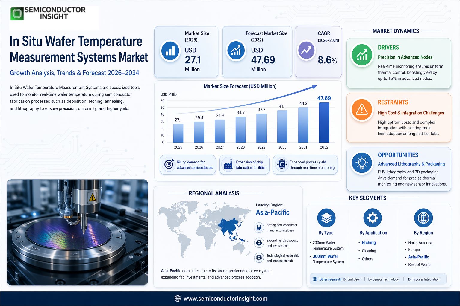
Global In Situ Wafer Temperature Measurement Systems market size was valued at USD 27.1 million in 2025. The market is projected to reach USD 47.69 million by 2032, exhibiting a CAGR of 8.6% during the forecast period.
In Situ Wafer Temperature Measurement Systems are specialized tools used in semiconductor manufacturing to monitor the real-time temperature of wafers during various fabrication processes. These systems are designed to ensure precise control of temperature, which is critical for achieving uniformity and consistency in processes like deposition, etching, annealing, and lithography.
The market is experiencing rapid growth due to several factors, including surging demand for advanced semiconductors, expansion in chip fabrication facilities, and the need for enhanced process yields. Furthermore, technological advancements in in-situ monitoring are driving adoption across etching, cleaning, and other applications. Key players such as KLA Corporation, CI Semi, k-Space Associates, Rsuwei, Guangdong Ruile Semiconductor Technology, and Shanghai Jheat Technology dominate the landscape with innovative portfolios and significant revenue shares.
MARKET DRIVERS
Precision Demands in Advanced Semiconductor Nodes
In Situ Wafer Temperature Measurement Systems Market is propelled by the semiconductor industry’s shift toward sub-5nm nodes, where temperature fluctuations of even 1°C can cause defects in deposition and etching processes. Real-time monitoring ensures uniform thermal profiles across wafers, boosting yield rates by up to 15% in high-volume manufacturing.
Expansion in AI and 5G Applications
Growth in AI accelerators and 5G infrastructure demands complex chip architectures, driving adoption of in situ systems for process control during plasma-enhanced chemical vapor deposition (PECVD). These tools enable fabs to achieve 98% process repeatability, supporting the projected 12% CAGR in semiconductor equipment through 2028.
➤ Increasing wafer sizes to 300mm and beyond necessitate advanced thermal metrology, with over 70% of leading-edge fabs integrating in situ temperature sensors.
Additionally, the surge in electric vehicle power semiconductors amplifies the need for reliable temperature data, fostering innovations in non-contact pyrometry and interferometry techniques within the market.
MARKET CHALLENGES
Technical Integration Complexities
Integrating in situ wafer temperature measurement into existing toolsets poses significant hurdles, as sensor calibration must withstand harsh plasma environments, leading to signal drift issues in 20-30% of installations. Compatibility with diverse process chambers further complicates deployment in multi-vendor fabs.
Other Challenges
High Development Costs
R&D expenses for robust, high-temperature sensors exceed $50 million per platform, straining smaller suppliers and slowing market penetration amid rising raw material costs for specialized optics and coatings.Supply chain disruptions for precision components, such as sapphire windows, exacerbate delays, with lead times stretching to 6-9 months and impacting 15% of new fab equipment orders globally.Moreover, achieving sub-micron spatial resolution remains elusive for low-k dielectric processes, where emissivity variations confound accuracy to within ±2°C.
MARKET RESTRAINTS
Cost Barriers and Economic Pressures
Elevated upfront costs, averaging $200,000-$500,000 per unit, restrain adoption among mid-tier foundries, particularly as capex budgets tighten amid global economic slowdowns projected to curb semiconductor investments by 5-7% in 2024.Dependency on legacy metrology infrastructure limits retrofitting, with 40% of older fabs relying on ex situ methods despite known yield losses, perpetuating a fragmented In Situ Wafer Temperature Measurement Systems Market.Intense competition from alternative proxy measurements, like plasma impedance monitoring, offers cheaper substitutes, capturing 25% of process control applications and capping growth in mature markets.Regulatory compliance for cleanroom emissions and material safety adds layers of validation, extending time-to-market by 12-18 months for new systems.
MARKET OPPORTUNITIES
Emerging Lithography and Packaging Trends
The transition to extreme ultraviolet (EUV) lithography creates demand for in situ systems capable of monitoring thermal gradients in high-NA scanners, poised to drive a 10% market uplift as EUV adoption reaches 50% of leading fabs by 2027.Advanced packaging techniques like chiplets and 3D stacking require precise interlayer temperature control, opening avenues for hybrid fiber-optic and wireless sensor integrations in heterogeneous manufacturing.Expansion in Asia-Pacific, with new gigafabs in India and Vietnam, presents untapped potential, targeting a regional market share increase from 35% to 45% through localized production of cost-effective pyrometers.AI-driven predictive analytics paired with in situ data analytics tools promise yield optimizations exceeding 20%, attracting investments from foundry leaders in next-gen process control.
In Situ Wafer Temperature Measurement Systems Market Trends
Enhanced Precision in Advanced Semiconductor Processes
In In Situ Wafer Temperature Measurement Systems Market, a dominant trend revolves around the demand for enhanced precision in advanced semiconductor manufacturing processes. These specialized systems provide real-time temperature monitoring of wafers during critical operations such as deposition, etching, annealing, and lithography. Precise temperature control is essential to achieve uniformity and consistency, directly impacting yield rates and device performance. As fabrication technologies evolve toward smaller nodes and complex structures, semiconductor manufacturers increasingly rely on these tools to mitigate thermal variations that could compromise process outcomes. Industry surveys highlight this shift, with experts noting stronger integration in high-volume production environments to support next-generation chip development.
Other Trends
Application Diversification Across Key Processes
Etching and cleaning applications dominate within In Situ Wafer Temperature Measurement Systems Market, reflecting their pivotal role in wafer fabrication workflows. Etching processes, in particular, benefit from in situ monitoring to maintain optimal plasma conditions and prevent defects, while cleaning steps ensure contaminant-free surfaces critical for subsequent layers. Other applications, including deposition variants, are gaining traction as manufacturers optimize multi-step sequences. This diversification underscores a broader trend toward process integration, where temperature measurement systems enable tighter control loops, reducing variability and enhancing overall fab efficiency.
Regional Expansion and Competitive Dynamics
Geographic expansion, especially in Asia with key hubs in China, Japan, and South Korea, characterizes In Situ Wafer Temperature Measurement Systems Market landscape. These regions host surging semiconductor capacities, driving demand for advanced metrology solutions amid global supply chain shifts. North America maintains a strong foothold through innovation-led adoption, complemented by Europe’s focus on specialized R&D. Competitively, players like KLA Corporation, CI Semi, k-Space Associates, Rsuwei, Guangdong Ruile Semiconductor Technology, and Shanghai Jheat Technology are advancing product lines tailored to 200mm and 300mm wafers. Their efforts address industry challenges such as process scalability and real-time analytics, fostering collaborative developments and market maturity while navigating supply constraints and technological hurdles.
COMPETITIVE LANDSCAPE
Key Industry Players
Leading Manufacturers in In Situ Wafer Temperature Measurement Systems Market
In Situ Wafer Temperature Measurement Systems Market is dominated by a few established players, with KLA Corporation holding a significant position due to its comprehensive portfolio in semiconductor metrology and process control solutions. The market structure is moderately concentrated, where the global top five players accounted for a substantial revenue share in 2025, reflecting their technological leadership in real-time temperature monitoring critical for semiconductor fabrication processes like etching, deposition, and annealing. KLA’s advanced systems ensure precise wafer temperature uniformity, supporting high-volume manufacturing for 200mm and 300mm wafers, amid a market projected to grow from US$27.1 million in 2025 to US$47.69 million by 2032 at a CAGR of 8.6%.
Beyond the leaders, several niche players contribute to innovation and regional competition, particularly in Asia-Pacific. Companies like CI Semi and k-Space Associates specialize in non-contact pyrometry and spectroscopic solutions tailored for in-situ applications, addressing demands in cleaning and other processes. Emerging Chinese firms such as Rsuwei, Guangdong Ruile Semiconductor Technology, and Shanghai Jheat Technology are gaining traction with cost-effective systems, expanding market accessibility. This dynamic fosters competition through R&D in optical and wireless measurement technologies, challenging incumbents while driving overall market advancements.
List of Key In Situ Wafer Temperature Measurement Systems Companies Profiled
- KLA Corporation
- CI Semi
- k-Space Associates
- Rsuwei
- Guangdong Ruile Semiconductor Technology
- Shanghai Jheat Technology
- layTec AG
- Accurion
- Film Sense
- Sentech Instruments
- EV Group (EVG)
- Nano-Master
- MKS Instruments
- PIKE Technologies
- Veeco Instruments
Segment Analysis:
| Segment Category | Sub-Segments | Key Insights |
| By Type |
|
Leading Segment: 300mm Wafer Temperature Measurement System
|
| By Application |
|
Leading Segment: Etching
|
| By End User |
|
Leading Segment: Semiconductor Foundries
|
| By Sensor Technology |
|
Leading Segment: Infrared Pyrometry
|
| By Process Integration |
|
Leading Segment: In-process Monitoring
|
Regional Analysis: In Situ Wafer Temperature Measurement Systems Market
Asia-Pacific
In Asia-Pacific, in situ wafer temperature measurement systems thrive through pioneering sensor fusion and AI-driven analytics. Leading fabs deploy infrared pyrometers and fiber-optic probes for millisecond response times, enabling proactive process adjustments. Collaborative innovation hubs in Singapore and Japan accelerate hybrid measurement platforms, integrating emissivity corrections for diverse wafer materials.
The region’s dense cluster of gigafabs drives ecosystem synergies, with suppliers co-locating to shorten lead times for in situ systems. Taiwan and South Korea’s vertical integration ensures seamless upgrades, while China’s scale-up creates cost-competitive calibration services, fortifying supply resilience in In Situ Wafer Temperature Measurement Systems Market.
Venture capital and state-backed funds pour into thermal metrology startups, spurring proprietary algorithms for multi-zone monitoring. Cross-border partnerships enhance interoperability, positioning Asia-Pacific as a launchpad for global standards in wafer temperature precision critical for logic and memory scaling.
Intense competition and talent shortages challenge sustained growth, yet initiatives like skill academies and IP protection frameworks mitigate risks. Evolving cleanroom protocols demand adaptive in situ solutions, reinforcing the region’s adaptive prowess in In Situ Wafer Temperature Measurement Systems Market.
North America
North America sustains a strong foothold in In Situ Wafer Temperature Measurement Systems Market, anchored by pioneering research institutions and equipment innovators in California and Oregon. Tech hubs prioritize R&D for quantum dot and photonics applications, where ultra-precise in situ monitoring addresses thermal instability in novel materials. Leading firms collaborate with defense contractors, customizing systems for high-reliability environments. Policy support for reshoring fabs stimulates demand, while academic-industry consortia advance predictive modeling. Nonetheless, higher costs temper volume adoption compared to Asia-Pacific peers.
Europe
Europe’s In Situ Wafer Temperature Measurement Systems Market reflects a blend of precision engineering heritage and sustainability imperatives. Germany and the Netherlands host advanced nodes focused on automotive and power electronics, leveraging in situ tech for uniform heating in SiC wafer processing. EU-funded projects emphasize eco-friendly sensors, reducing energy footprints. Fragmented supply chains pose hurdles, but strategic mergers enhance competitiveness, positioning Europe as a quality leader amid green manufacturing transitions.
South America
South America trails in In Situ Wafer Temperature Measurement Systems Market, with nascent semiconductor efforts centered in Brazil. Emerging assembly-test facilities explore in situ adoption for legacy nodes serving consumer electronics. Infrastructure limitations hinder progress, yet regional partnerships with Asian suppliers introduce affordable solutions. Growing EV ambitions could catalyze uptake, fostering skill development and local customization to bridge the technology gap.
Middle East & Africa
The Middle East & Africa region shows tentative strides in In Situ Wafer Temperature Measurement Systems Market, buoyed by UAE and Israel’s innovation corridors. Specialized fabs target sensors and discretes, integrating in situ tools for harsh-environment resilience. Oil-funded diversification spurs investments, while African tech parks eye assembly roles. Geopolitical stability and talent pipelines will dictate acceleration in this evolving landscape.
Report Scope
This market research report provides a comprehensive analysis of the In Situ Wafer Temperature Measurement Systems Market , covering the forecast period 2026–2034. It offers detailed insights into market dynamics, technological advancements, competitive landscape, and key trends shaping the industry.
Key focus areas of the report include:
- Market Overview: The report begins with an overview outlining its current market scenario, key growth indicators, and industry transformation drivers. It discusses macroeconomic factors, demand–supply balance, regulatory landscape, and the strategic role of semiconductors in powering advancements across industries such as automotive, telecommunications, consumer electronics, and industrial automation.
- Market Size & Forecast: Historical data and future projections for revenue, unit shipments, and market value across major regions and segments.
- Segmentation Analysis: Detailed breakdown by product type, technology, application, and end-user industry to identify high-growth segments and investment opportunities.
- Regional Insights: Insights into market performance across North America, Europe, Asia-Pacific, Latin America, and the Middle East & Africa, including country-level analysis where relevant.
- Competitive Landscape: Profiles of leading market participants, including their product offerings, R&D focus, manufacturing capacity, pricing strategies, and recent developments such as mergers, acquisitions, and partnerships.
- Technology Trends & Innovation: Assessment of emerging technologies, integration of AI/IoT, semiconductor design trends, fabrication techniques, and evolving industry standards.
- Market Drivers & Restraints: Evaluation of factors driving market growth along with challenges, supply chain constraints, regulatory issues, and market-entry barriers.
- Stakeholder Insights: Insights for component suppliers, OEMs, system integrators, investors, and policymakers regarding the evolving ecosystem and strategic opportunities.
Primary and secondary research methods are employed, including interviews with industry experts, data from verified sources, and real-time market intelligence to ensure the accuracy and reliability of the insights presented.
FREQUENTLY ASKED QUESTIONS:
What is the current market size of In Situ Wafer Temperature Measurement Systems Market?
-> In Situ Wafer Temperature Measurement Systems Market was valued at USD 27.1 million in 2025 and is expected to reach USD 47.69 million by 2032, at a CAGR of 8.6% during the forecast period.
Which key companies operate in In Situ Wafer Temperature Measurement Systems Market?
-> Key players include KLA Corporation, CI Semi, k-Space Associates, Rsuwei, Guangdong Ruile Semiconductor Technology, Shanghai Jheat Technology, among others.
What are the key growth drivers?
-> Key growth drivers include demand for precise real-time temperature monitoring in semiconductor fabrication processes like deposition, etching, annealing, and lithography, and advancements in semiconductor manufacturing technologies.
Which region dominates the market?
-> Asia is the fastest-growing region, particularly China, Japan, and South Korea, while North America holds significant market share.
What are the emerging trends?
-> Emerging trends include shift to 300mm wafer temperature measurement systems, integration in etching and cleaning applications, and enhanced non-contact measurement technologies.

Get Sample Report PDF for Exclusive Insights
Report Sample Includes
- Table of Contents
- List of Tables & Figures
- Charts, Research Methodology, and more...


