
MARKET INSIGHTS
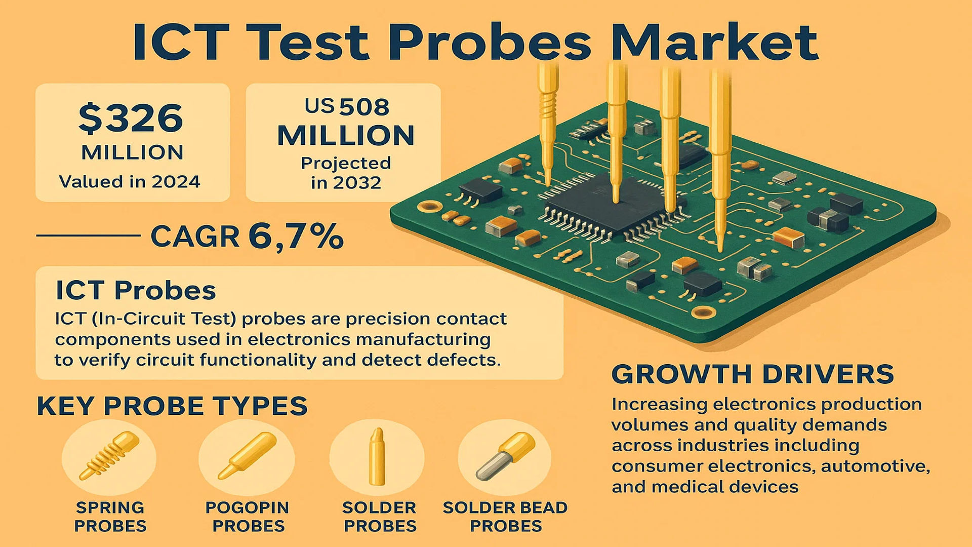
The global ICT Test Probes Market was valued at 326 million in 2024 and is projected to reach US$ 508 million by 2032, at a CAGR of 6.7% during the forecast period.
ICT (In-Circuit Test) probes are precision contact components used in electronics manufacturing to verify circuit functionality and detect defects such as open circuits, short circuits, and faulty components. These probes enable rapid electrical testing of printed circuit board assemblies (PCBAs) by making temporary electrical connections to test points, measuring parameters like resistance, voltage, and current. Key probe types include spring probes, pogopin probes, and solder bead probes, each offering different durability and conductivity characteristics.
Market growth is driven by increasing electronics production volumes and quality demands across industries including consumer electronics, automotive, and medical devices. The expansion of semiconductor wafer testing and advanced packaging technologies like 2.5D/3D ICs is creating new application areas. However, rising complexity of PCBA designs and miniaturization trends require continuous probe technology improvements, particularly in high-frequency testing applications. Leading manufacturers are addressing these challenges through advanced materials like beryllium copper alloys and specialized platings to enhance durability and signal integrity.
MARKET DYNAMICS
MARKET DRIVERS
Accelerated Growth in Semiconductor and Electronics Manufacturing to Drive Market Expansion
The global ICT test probes market is experiencing robust growth driven by the rapid expansion of semiconductor and electronics manufacturing. With the electronics industry projected to grow exponentially due to increasing demand for smart devices, IoT solutions, and advanced consumer electronics, the need for precise testing solutions has intensified. Modern IC designs with finer geometries and higher pin densities require more sophisticated probing solutions, pushing manufacturers to innovate and produce probes capable of handling densities up to 25,000 probes per square centimeter. The continuous miniaturization of electronic components, coupled with the integration of AI and 5G technologies, has significantly raised testing complexity, thereby driving demand for advanced ICT probes.
Automotive Electronics Revolution Creating New Demand for High-Temperature Probes
The automotive sector’s transition toward electrification and autonomous driving systems has created substantial demand for specialized ICT test probes capable of withstanding extreme conditions. Modern vehicles incorporate over 3,000 semiconductor chips on average, each requiring thorough testing. The growing complexity of automotive electronics, including ADAS systems and EV battery management, necessitates probes that can operate reliably in temperature ranges from -40°C to 150°C. This sector’s stringent quality requirements and the automotive industry’s 0 ppm defect tolerance policies have accelerated adoption of premium testing solutions featuring gold-plated or tungsten carbide tips for enhanced durability.
Advancements in Probe Technology Enhancing Testing Efficiency
Technological innovations in probe design and materials are significantly contributing to market growth. Recent developments include micro-machined spring probes with lifespans exceeding 500,000 contact cycles and hybrid probe designs combining multiple testing technologies. The introduction of MEMS-based probes has enabled testing at frequencies above 10 GHz, critical for 5G and millimeter-wave applications. Furthermore, smart probes with built-in sensors can now provide real-time performance data, reducing test time by up to 30% compared to conventional solutions. These technological improvements are driving replacement cycles and encouraging manufacturers to upgrade their testing infrastructure.
MARKET RESTRAINTS
High Initial Investment and Cost Sensitivity in Price-Competitive Markets
While the ICT test probes market shows strong growth potential, high equipment costs present a significant barrier to adoption. Premium test probes with advanced materials and coatings can cost 3-5 times more than standard solutions, making them prohibitive for small and medium-sized manufacturers. The total cost of ownership for advanced probing systems, including maintenance and replacement parts, often exceeds $250,000 annually for high-volume production facilities. This financial barrier is particularly challenging in price-sensitive markets where manufacturers prioritize short-term cost savings over long-term quality assurance investments.
Technical Challenges in Miniaturization Testing
The industry faces mounting technical challenges as component sizes continue to shrink. Testing advanced packaging technologies like 3D ICs and wafer-level chip scale packages requires probes with tip diameters below 20 microns while maintaining electrical performance. Current limitations in micro-machining technology make production of such probes both technically challenging and economically inefficient. Additionally, the increasing use of low-K dielectric materials in semiconductor fabrication creates probing difficulties due to their mechanical fragility, often resulting in yield losses during testing.
Supply Chain Complexities Impacting Lead Times
Global supply chain disruptions have significantly impacted the availability of rare metals and specialized materials used in high-performance test probes. Tungsten and beryllium copper, essential for probe manufacturing, face periodic shortages that can extend lead times to 6-8 months for certain probe types. The concentration of specialty material suppliers in limited geographic regions creates vulnerabilities in the supply chain, forcing probe manufacturers to maintain large inventories that tie up working capital.
MARKET CHALLENGES
Skilled Labor Shortage in Precision Manufacturing
The industry faces a critical shortage of skilled technicians capable of operating and maintaining advanced probing systems. Precision probe manufacturing requires specialized knowledge in materials science, micro-mechanics, and electrical engineering. The current workforce gap is estimated to exceed 25% of total demand in developed markets. This skills shortage is compounded by lengthy training periods (6-12 months) required to achieve proficiency in probe assembly and maintenance operations, creating bottlenecks in production and service delivery.
Compatibility Issues in Heterogeneous Integration Testing
The rise of heterogeneous integration in semiconductor packaging presents new testing challenges. Combining disparate technologies like logic, memory, and sensors in single packages requires probes capable of handling different voltage levels and signal types simultaneously. Current probe card designs often struggle with cross-talk and signal integrity issues in these complex testing environments. The lack of standardized testing protocols for advanced packaging further complicates probe design optimization, leading to extended development cycles and increased R&D expenditures.
Environmental Regulations Impacting Material Selection
Stringent environmental regulations, particularly REACH and RoHS compliance in major markets, are restricting the use of certain materials traditionally employed in probe manufacturing. The phasing out of lead-based alloys and certain nickel compounds has forced manufacturers to develop alternative plating solutions that often compromise performance characteristics. Compliance with evolving regulations adds 15-20% to material development costs and requires continuous reformulation of probe components to meet changing environmental standards across different regions.
MARKET OPPORTUNITIES
Emerging Advanced Packaging Technologies Creating New Testing Requirements
The rapid development of advanced packaging technologies such as chiplets and 3D system-in-package designs is creating substantial opportunities for probe manufacturers. These packaging approaches require novel testing methodologies, driving demand for specialized probe cards capable of simultaneous multi-die testing. The advanced packaging market’s projected growth creates significant potential for probes featuring micro-spring arrays and MEMS-based contact solutions. Manufacturers developing proprietary solutions for these emerging applications can capture premium pricing and establish long-term technology partnerships with leading semiconductor companies.
Expansion of 5G Infrastructure Driving High-Frequency Probe Demand
Global 5G network deployments are generating strong demand for high-frequency test probes capable of handling millimeter-wave signals. The need for testing RF front-end modules operating above 28 GHz is creating a specialized market segment for probes with advanced signal integrity characteristics. This represents a high-margin opportunity as RF probes typically command 30-50% price premiums over standard solutions. The ongoing rollout of 5G infrastructure and subsequent generations of wireless technology ensures sustained demand for these specialized testing solutions throughout the forecast period.
Smart Manufacturing Trends Enabling Predictive Maintenance Solutions
The integration of Industry 4.0 technologies in test environments presents opportunities for smart probe solutions with embedded sensors and connectivity. Probes capable of real-time wear monitoring and predictive maintenance can reduce unplanned downtime by up to 40% in high-volume manufacturing facilities. The development of cloud-connected probe management systems allows for centralized performance monitoring across global production networks. This digital transformation trend enables probe manufacturers to transition from product suppliers to service providers offering comprehensive testing solutions with performance guarantees and data analytics capabilities.
ICT TEST PROBES MARKET TRENDS
Miniaturization of Electronic Components Driving Demand for High-Precision Probes
The rapid miniaturization of electronic components has significantly influenced the ICT test probes market, as manufacturers require probes capable of testing increasingly compact and densely packed printed circuit boards (PCBs). With innovations such as BGA (Ball Grid Array) and CSP (Chip Scale Package) gaining traction, the demand for finer-pitch probes with diameters below 0.2mm has surged. Probes with superior electrical performance and mechanical durability are now essential to ensure reliable testing in high-frequency applications, including 5G devices and automotive electronics. Furthermore, the emergence of flexible electronics and foldable displays has prompted the development of specialized probes for non-rigid substrates.
Other Trends
Automation in Semiconductor Testing
The shift toward automation in semiconductor testing facilities has fueled the adoption of advanced probe cards and automated test equipment (ATE) solutions. Probes with self-cleaning capabilities and longer lifespans are becoming indispensable for high-volume manufacturing environments. The growing complexity of IC designs, particularly in AI and IoT chips, necessitates multi-DUT (Device Under Test) testing configurations, thereby accelerating the deployment of modular probe solutions.
Sustainability and Material Innovation Reshaping Probe Manufacturing
Environmental regulations and corporate sustainability goals are pushing manufacturers to explore eco-friendly materials such as lead-free alloys and recyclable tungsten-carbide composites. Simultaneously, gold-plated probes remain dominant for high-reliability applications despite cost pressures, while alternatives like palladium-nickel coatings gain traction in cost-sensitive segments. The market is witnessing increased R&D investments in wear-resistant coatings that extend probe lifespan by up to 30%, directly reducing electronic waste from frequent replacements. These material advancements coincide with stricter industry standards for probe conductivity and contact resistance in mission-critical applications like medical device testing.
COMPETITIVE LANDSCAPE
Key Industry Players
Innovation and Precision Drive Market Leadership in ICT Test Probes
The global ICT test probes market features a dynamic competitive environment with a mix of established multinational corporations and specialized manufacturers. INGUN Prüfmittelbau GmbH and Feinmetall GmbH are dominant forces in the industry, leveraging their German engineering expertise to deliver high-performance probes with exceptional durability. These companies collectively account for over 30% of the global market share, owing to their ability to serve demanding applications in automotive and semiconductor testing.
LEENO Industrial Inc has emerged as a key Asian contender, capturing significant market traction through cost-effective manufacturing and rapid product customization capabilities. Their strong presence in South Korea’s thriving electronics sector has enabled consistent revenue growth. Meanwhile, Smiths Interconnect maintains competitive advantage through strategic acquisitions and proprietary contact technologies that enhance signal integrity in high-frequency applications.
The market sees increasing competition from emerging players like Chip Shine Technology and TESPRO Co.,Ltd, who are gaining recognition for innovative probe designs compatible with advanced packaging technologies. These challengers are particularly successful in addressing the evolving needs of wafer-level testing, where precise probe card solutions are critical.
Major corporations are actively expanding their portfolios through both organic R&D and strategic partnerships. Everett Charles Technologies recently launched a new series of high-current probes, while PTR HARTMANN GmbH introduced patented self-cleaning probe tips that significantly extend operational lifespan in harsh testing environments.
List of Key ICT Test Probe Manufacturers
- INGUN Prüfmittelbau GmbH (Germany)
- Feinmetall GmbH (Germany)
- LEENO Industrial Inc (South Korea)
- Smiths Interconnect (U.K.)
- Everett Charles Technologies Inc (U.S.)
- PTR HARTMANN GmbH (Germany)
- C.C.P Contact Probes (Japan)
- KITA Manufacturing Co.,Ltd. (Japan)
- Chip Shine Technology (Taiwan)
- ATX Hardware GmbH West (Germany)
- Columbia Elektronik AB (Sweden)
- TESPRO Co.,Ltd (China)
Segment Analysis:
By Type
Spring Probe Segment Dominates Due to High Durability and Precision in PCB Testing
The market is segmented based on type into:
- Spring Probe
- Subtypes: Standard, High-Current, and others
- Pogopin Probe
- Solder Bead Probe
By Application
Semiconductor Testing Segment Leads Owning to Rising Demand for Advanced Chip Packaging Technologies
The market is segmented based on application into:
- Semiconductor Testing
- Subtypes: Wafer-level testing, Package testing
- Automotive Testing
- PCB Testing
- Others
By End-User
Electronics Manufacturing Sector Accounts for Largest Share Due to High Volume PCB Production
The market is segmented based on end-user into:
- Consumer Electronics Manufacturers
- Automotive Electronics Suppliers
- Medical Device Companies
- Telecom Equipment Providers
Regional Analysis: ICT Test Probes Market
Asia-Pacific
Asia-Pacific dominates the global ICT test probes market, driven by robust electronics manufacturing hubs in China, Japan, South Korea, and Taiwan. The region accounts for over 45% of global demand due to extensive semiconductor fabrication and PCB production facilities. China’s semiconductor self-sufficiency push, including its $150 billion investment plan, accelerates probe adoption for chip testing applications. While Japan leads in high-precision probe manufacturing, Southeast Asian nations are emerging as cost-effective production bases. Key challenges include component miniaturization pressures and the need for probe durability enhancements to meet automotive-grade testing standards.
North America
North America’s ICT test probe market thrives on advanced semiconductor testing requirements and stringent quality standards in aerospace/defense applications. The U.S. holds 78% regional market share, with major probe manufacturers like Everett Charles Technologies serving automotive EV testing needs. The CHIPS Act’s $52 billion funding bolsters domestic semiconductor production, subsequently driving probe demand for wafer-level testing. Canadian markets show growing adoption in medical device manufacturing, where high-reliability probe requirements are critical. The region prioritizes customized probe solutions for 5G infrastructure and AI hardware testing applications.
Europe
Europe maintains a technology-driven ICT test probe market, led by Germany’s automotive electronics sector and the Netherlands’ semiconductor equipment industry. EU initiatives like the Chips Act stimulate probe demand for advanced packaging testing, particularly for IoT and industrial automation components. INGUN and Feinmetall lead in developing compliant solutions for RoHS and REACH standards. While Western Europe focuses on high-margin precision probes, Eastern European nations are emerging as probe assembly hubs. The market faces margin pressures from Asian competitors but maintains advantages in specialized applications like MEMS testing.
South America
South America’s ICT test probe market shows moderate growth, concentrated in Brazil’s automotive electronics and Argentina’s appliance manufacturing sectors. Local production remains limited, with over 65% of probes imported from Asia. The lack of advanced semiconductor facilities restricts high-end probe applications, though PCB testing demand grows steadily. Economic volatility affects capital expenditures on testing equipment, but increasing smartphone adoption drives basic probe requirements. Opportunities exist in servicing Brazil’s revived semiconductor packaging initiatives and Chile’s renewable energy electronics sector.
Middle East & Africa
The MEA region represents an emerging ICT test probe market, with growth pockets in Israel’s semiconductor design ecosystem and UAE’s electronics assembly plants. Israel’s test probe demand stems from military/aerospace applications, while South Africa serves as a gateway for automotive probe imports. Limited local manufacturing capability creates dependency on European and Asian suppliers. Market expansion faces hurdles from low electronics production volumes, though increasing investments in telecom infrastructure and smart city projects present long-term opportunities for basic PCB testing solutions.
Report Scope
This market research report provides a comprehensive analysis of the global ICT Test Probes market, covering the forecast period 2025–2032. It offers detailed insights into market dynamics, technological advancements, competitive landscape, and key trends shaping the industry.
Key focus areas of the report include:
- Market Size & Forecast: Historical data and future projections for revenue, unit shipments, and market value across major regions and segments. The global ICT Test Probes market was valued at USD 326 million in 2024 and is projected to reach USD 508 million by 2032, growing at a CAGR of 6.7%.
- Segmentation Analysis: Detailed breakdown by product type (Spring Probe, Pogopin Probe, Solder Bead Probe), application (Semiconductor Testing, Automotive Testing, PCB Testing), and end-user industry to identify high-growth segments.
- Regional Outlook: Insights into market performance across North America, Europe, Asia-Pacific, Latin America, and the Middle East & Africa, with Asia-Pacific dominating due to strong electronics manufacturing growth.
- Competitive Landscape: Profiles of 12 leading market participants including LEENO Industrial Inc, INGUN Prüfmittelbau GmbH, Smiths Interconnect, and Feinmetall GmbH, covering their market share, product portfolios, and strategic initiatives.
- Technology Trends & Innovation: Assessment of advanced probe designs, specialized coatings for enhanced durability, and integration with automated test systems.
- Market Drivers & Restraints: Evaluation of factors including growth in electronics manufacturing, wafer production expansion, alongside challenges like material cost volatility.
- Stakeholder Analysis: Strategic insights for semiconductor manufacturers, test equipment providers, and investors regarding the evolving testing ecosystem.
The analysis employs both primary research (industry expert interviews) and secondary research (verified market data) to ensure accuracy and reliability.
FREQUENTLY ASKED QUESTIONS:
What is the current market size of Global ICT Test Probes Market?
-> ICT Test Probes Market was valued at 326 million in 2024 and is projected to reach US$ 508 million by 2032, at a CAGR of 6.7% during the forecast period.
Which key companies operate in Global ICT Test Probes Market?
-> Key players include LEENO Industrial Inc, INGUN Prüfmittelbau GmbH, Smiths Interconnect, Feinmetall GmbH, PTR HARTMANN GmbH, and Everett Charles Technologies, among others.
What are the key growth drivers?
-> Primary drivers include expansion of semiconductor manufacturing, increasing PCB complexity, and growing demand for high-precision testing solutions in automotive and consumer electronics.
Which region dominates the market?
-> Asia-Pacific holds the largest market share (over 45% in 2024), driven by electronics manufacturing hubs in China, Japan, and South Korea.
What are the emerging trends?
-> Emerging trends include miniaturized probe designs, advanced material coatings for extended lifespan, and integration with Industry 4.0 test systems.

Get Sample Report PDF for Exclusive Insights
Report Sample Includes
- Table of Contents
- List of Tables & Figures
- Charts, Research Methodology, and more...
 Download Sample Report PDF






