Market Insights
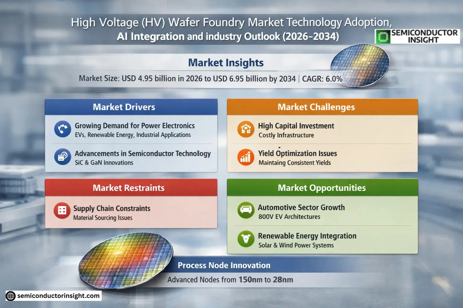
Global High Voltage (HV) Wafer Foundry Market size was valued at USD 4.66 billion in 2025. The market is projected to grow from USD 4.95 billion in 2026 to USD 6.95 billion by 2034, exhibiting a CAGR of 6.0% during the forecast period.
High Voltage (HV) wafer foundries specialize in manufacturing semiconductor wafers capable of handling elevated voltage levels, typically above 20V, for applications such as power management ICs, display drivers, and automotive electronics. These foundries utilize specialized process nodes ranging from legacy 150nm technologies to advanced 28nm nodes, enabling optimized performance for high-voltage applications while balancing power efficiency and cost.
The market growth is driven by increasing demand for energy-efficient power management solutions across consumer electronics and electric vehicles, coupled with advancements in display technologies requiring precise high-voltage driver ICs. Leading foundries like TSMC and Samsung are expanding their HV technology portfolios through node shrinks and material innovations to address growing requirements from automotive and industrial sectors where reliability under high-voltage conditions is critical.
MARKET DRIVERS
Growing Demand for Power Electronics
High Voltage (HV) Wafer Foundry Market is experiencing significant growth due to increasing demand for power electronics in electric vehicles, renewable energy systems, and industrial applications. The transition to energy-efficient technologies has accelerated adoption of HV wafer solutions.
Advancements in Semiconductor Technology
Breakthroughs in silicon carbide (SiC) and gallium nitride (GaN) wafer fabrication have enabled higher voltage tolerance and improved thermal performance, driving market expansion. Foundries are investing heavily in specialized HV process nodes to meet growing demand.
Government initiatives for energy infrastructure modernization are creating additional demand for HV wafer solutions in smart grid applications and power transmission systems.
MARKET CHALLENGES
High Capital Investment Requirements
Establishing HV wafer foundries requires substantial investments in specialized equipment and cleanroom facilities. The barrier to entry remains high, with only established players able to maintain the necessary infrastructure.
Other Challenges
Yield Optimization
Maintaining consistent yields for HV wafers presents technical challenges due to the precision required in doping and etching processes at higher voltage thresholds.
MARKET RESTRAINTS
Supply Chain Constraints
High Voltage (HV) Wafer Foundry Market faces material sourcing challenges, particularly for silicon carbide substrates. Geopolitical factors and limited substrate suppliers create bottlenecks in production capacity expansion.
MARKET OPPORTUNITIES
Expansion in Automotive Sector
The automotive industry’s shift toward 800V architectures for electric vehicles presents significant growth potential for HV wafer foundries. This transition requires specialized wafer solutions capable of handling higher voltage requirements.
Renewable Energy Integration
Growing investments in solar and wind energy systems are driving demand for HV power conversion solutions, creating new opportunities for foundries specializing in high-voltage wafer processing.
High Voltage (HV) Wafer Foundry Market Trends
Process Node Innovation Driving Market Growth
High Voltage (HV) Wafer Foundry Market is witnessing significant advancements in process node technology. Leading foundries like TSMC and Samsung are offering HV processes ranging from 0.5µm to 28nm, enabling higher quality imaging for display drivers. These smaller nodes provide improved power efficiency for applications across TVs, smartphones, tablets, and wearables.
Other Trends
Expansion of OLED and LCD Display Applications
HV wafer foundries are experiencing growing demand due to the rising adoption of OLED and LCD display technologies. Samsung Foundry’s HV processes (130nm to 28nm) are particularly suited for creating advanced display drivers that enhance visual quality in consumer electronics.
Geographic Market Shifts
The Asia-Pacific region continues to dominate High Voltage (HV) Wafer Foundry Market, with China emerging as a key growth area. This geographic concentration aligns with the region’s strong semiconductor manufacturing ecosystem and increasing demand for display technologies in consumer electronics production.
Wafer Size Transition in Production
There’s a noticeable shift toward larger wafer sizes in HV foundry operations, with 12-inch wafers gaining market share over 8-inch alternatives. This transition is driven by the need for greater production efficiency and cost reduction in high-volume manufacturing.
Competitive Landscape Evolution
The market remains concentrated among major players including TSMC, Samsung Foundry, and UMC, which collectively hold significant revenue share. These companies are investing in process refinement and capacity expansion to maintain their market positions in the High Voltage Wafer Foundry segment.
COMPETITIVE LANDSCAPE
Key Industry Players
TSMC and Samsung Dominate High Voltage Wafer Foundry Market with Advanced Process Nodes
Taiwan Semiconductor Manufacturing Company (TSMC) leads Global High Voltage (HV) Wafer Foundry Market with its advanced 28nm HV processes, commanding significant market share through superior power efficiency solutions for display drivers. Samsung Foundry follows closely with its competitive 28nm-130nm HV process portfolio, particularly strong in OLED display driver applications. The market exhibits an oligopolistic structure where the top five players collectively control over 70% revenue share, with UMC and VIS emerging as strong regional contenders in specialized process nodes.
Niche players like HLMC and Nexchip are gaining traction in the Chinese market through government-backed semiconductor initiatives, focusing on cost-effective 90nm-150nm HV solutions. Emerging foundries such as GlobalFoundries and SMIC are strategically expanding their HV capabilities to capture growing demand for automotive and industrial applications, though currently trailing behind market leaders in process sophistication and production scale.
List of Key High Voltage (HV) Wafer Foundry Companies Profiled
- Taiwan Semiconductor Manufacturing Company (TSMC)
- Samsung Foundry
- United Microelectronics Corporation (UMC)
- Vanguard International Semiconductor (VIS)
- HLMC (Huahong Grace Semiconductor)
- Nexchip Semiconductor
- GlobalFoundries
- Semiconductor Manufacturing International Corporation (SMIC)
- Tower Semiconductor
- DB HiTek
- Powerchip Semiconductor Manufacturing Corporation
- X-FAB Silicon Foundries
- MagnaChip Semiconductor
- Shanghai Huali Microelectronics Corporation
- SilTerra Malaysia
Segment Analysis:
| Segment Category | Sub-Segments | Key Insights |
| By Type |
|
45nm and Below represents the most advanced process node with superior image quality and power efficiency:
|
| By Application |
|
TVs dominate HV wafer foundry demand due to:
|
| By End User |
|
Display Panel Makers account for the largest share:
|
| By Process Node |
|
Advanced Nodes show strongest growth potential:
|
| By Wafer Size |
|
12-inch Wafer production dominates the market:
|
Regional Analysis: High Voltage (HV) Wafer Foundry Market
Taiwan controls over 60% of global HV wafer foundry capacity through TSMC and specialized players like Vanguard. The island’s ecosystem excels in high-voltage BCD (Bipolar-CMOS-DMOS) processes critical for power management ICs. Continuous node migration to 40nm HV platforms supports denser integration.
Chinese foundries like SMIC and Hua Hong Semiconductor are rapidly building HV wafer capacity with government backing. Focus areas include 200mm wafer production for automotive chips and infrastructure projects. Localization policies drive adoption of domestic HV solutions in smart grid applications.
South Korean players leverage advanced packaging and wide-bandgap material expertise. Samsung Foundry’s 28nm HV RF platform targets 5G infrastructure, while DB HiTek specializes in high-voltage display driver ICs. Government-private partnerships accelerate GaN-on-Si wafer development.
Japan maintains leadership in high-reliability HV wafers for industrial and automotive applications. Foundries like Tower Semiconductor leverage legacy power device knowledge. Collaboration between equipment makers and material suppliers strengthens process innovation in high-voltage SOI technologies.
North America
The North American HV wafer foundry market benefits from strong R&D ecosystems and defense/aerospace demand. GlobalFoundries’ Burlington fab specializes in high-voltage SOI processes, while Texas Instruments maintains internal HV capacity. The region sees growing demand for HV wafers in renewable energy inverters and EV charging infrastructure. U.S. CHIPS Act funding is accelerating domestic HV foundry investments, particularly in wide-bandgap semiconductor production. Collaborative R&D between national labs and foundries focuses on next-generation HV materials.
Europe
Europe’s HV wafer foundry sector concentrates on automotive and industrial applications. STMicroelectronics’ BCD processes lead in smart power applications, while X-FAB provides specialized HV CMOS solutions. The region benefits from strong automotive OEM-supplier networks demanding high-reliability power devices. EU semiconductor initiatives prioritize HV technologies for energy-efficient systems. Research collaborations focus on integrating HV wafer processes with MEMS sensors for Industry 4.0 applications.
Middle East & Africa
MEA shows emerging potential in HV wafer foundry services through strategic investments. Saudi Arabia’s Vision 2030 includes semiconductor manufacturing plans with potential HV wafer specialization. The region’s focus on renewable energy projects drives demand for power management ICs. Limited domestic foundry presence necessitates reliance on imports, though technology transfer agreements with Asian foundries are increasing.
South America
South America’s HV wafer needs are primarily served through imports, with growing local assembly of power electronics. Brazil shows potential for HV wafer backend services, leveraging automotive manufacturing bases. Regional challenges include limited semiconductor infrastructure, though governments are exploring partnerships to develop basic foundry capabilities tailored for power device packaging and testing.
Report Scope
This market research report provides a comprehensive analysis of the High Voltage (HV) Wafer Foundry Market, covering the forecast period 2025–2034. It offers detailed insights into market dynamics, technological advancements, competitive landscape, and key trends shaping the industry.
Key focus areas of the report include:
- Market Overview: The report begins with an overview outlining its current market scenario, key growth indicators, and industry transformation drivers. It discusses macroeconomic factors, demand–supply balance, regulatory landscape, and the strategic role of semiconductors in powering advancements across industries such as automotive, telecommunications, consumer electronics, and industrial automation.
- Market Size & Forecast: Historical data and future projections for revenue, unit shipments, and market value across major regions and segments.
- Segmentation Analysis: Detailed breakdown by product type, technology, application, and end-user industry to identify high-growth segments and investment opportunities.
- Regional Insights: Insights into market performance across North America, Europe, Asia-Pacific, Latin America, and the Middle East & Africa, including country-level analysis where relevant.
- Competitive Landscape: Profiles of leading market participants, including their product offerings, R&D focus, manufacturing capacity, pricing strategies, and recent developments such as mergers, acquisitions, and partnerships.
- Technology Trends & Innovation: Assessment of emerging technologies, integration of AI/IoT, semiconductor design trends, fabrication techniques, and evolving industry standards.
- Market Drivers & Restraints: Evaluation of factors driving market growth along with challenges, supply chain constraints, regulatory issues, and market-entry barriers.
- Stakeholder Insights: Insights for component suppliers, OEMs, system integrators, investors, and policymakers regarding the evolving ecosystem and strategic opportunities.
Primary and secondary research methods are employed, including interviews with industry experts, data from verified sources, and real-time market intelligence to ensure the accuracy and reliability of the insights presented.
FREQUENTLY ASKED QUESTIONS:
What is the current market size of High Voltage (HV) Wafer Foundry Market?
-> High Voltage (HV) Wafer Foundry Market size was valued at USD 4.66 billion in 2025. The market is projected to grow from USD 4.95 billion in 2026 to USD 6.95 billion by 2034, exhibiting a CAGR of 6.0% during the forecast period.
Which key companies operate in High Voltage (HV) Wafer Foundry Market?
-> Key players include TSMC, Samsung Foundry, United Microelectronics Corporation (UMC), VIS (Vanguard International Semiconductor), HLMC, and Nexchip, among others.
What are the key growth drivers?
-> Key growth drivers include increasing demand for high-quality display drivers in consumer electronics, adoption of advanced semiconductor fabrication technologies, and rising investments in automotive and industrial automation sectors.
Which region dominates the market?
-> Asia-Pacific is the dominant market, driven by high semiconductor manufacturing activities in China, Japan, and South Korea.
What are the emerging trends?
-> Emerging trends include adoption of smaller process nodes (45nm and below), development of energy-efficient wafer solutions, and expansion of 12-inch wafer foundry capacity.
Get Sample Report PDF for Exclusive Insights
Report Sample Includes
- Table of Contents
- List of Tables & Figures
- Charts, Research Methodology, and more...
 Download Sample Report PDF