SEMICONDUCTOR INSIGHT
MARKET RESEARCH REPORT

High-end IC Substrate Market

2026 to 2034
MARKET INTELLIGENCE
ACROSS KEY REGIONS
2026 EDITION
INTEGRATED CIRCUITS Semiconductor Market Research

High-end IC Substrate Market

Trends, Business Strategies 2026-2034

◷
UPDATED 18 September 2026
▤
REPORT LENGTH Detailed Report
▣
REPORT CODE fbdfb5e329c4
▯
FORMATS PDF

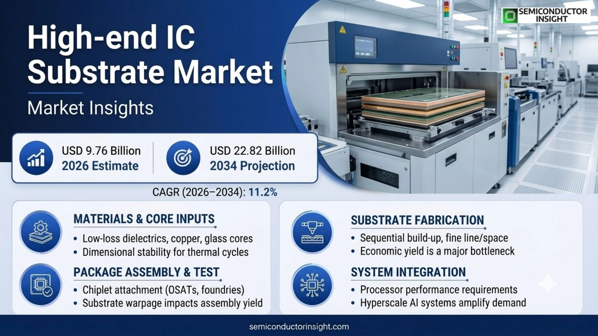
High-end IC Substrate Market was reaches USD 22.82 billion by 2034, equal to a 11.2% CAGR during 2026–2034. The 2026 estimated value is USD 9.76 billion. Asia Pacific is the largest market and manufacturing center because Taiwan, Japan, South Korea, China and Malaysia contain the deepest IC-substrate capacity, advanced packaging ecosystems and customer qualification networks.

Get the sample PDF with study scope, segmentation and methodology details.

Key Statistics

2025 Market Size
USD 8.77 billion
2034 Projected Size
USD 22.82 billion
CAGR (2026–2034)
11.2%
Largest Market in 2025
Asia Pacific

Key Takeaways

  • Complex FC BGA substrates are the largest type, supported by CPUs, GPUs, AI accelerators and high-performance computing packages that require large body sizes and dense routing.
  • 3C electronics remains the largest application in the source segmentation, while AI servers and telecom infrastructure are shifting incremental investment toward larger, higher-layer-count FC BGA formats.
  • Organic substrates hold the majority material position because they combine manufacturability, routing density and cost at the scale required by advanced package assembly.
  • Asia Pacific is the largest regional market and production center, with the supply base concentrated across Taiwan, Japan, South Korea, China and increasingly Malaysia.
  • AI infrastructure is the strongest structural driver: substrate makers are adding capacity for larger form factors, finer features and more build-up layers tied to high-performance server demand.
  • Geographic concentration is the central strategic risk: U.S. advanced-packaging programs and new glass-substrate investment seek to broaden a supply chain that remains heavily centered in Asia.

High-end IC Substrate Market Overview

High-end IC Substrate Market was valued at USD 8.77 billion in 2025. Rebased from the report page’s published size anchors, the standardized series reaches USD 22.82 billion by 2034, equal to a 11.2% CAGR during 2026–2034. The 2026 estimated value is USD 9.76 billion. Asia Pacific is the largest market and manufacturing center because Taiwan, Japan, South Korea, China and Malaysia contain the deepest IC-substrate capacity, advanced packaging ecosystems and customer qualification networks.

Base year: 2025 · Estimated year: 2026 · Forecast period: 2026–2034 · Values in USD

High-end IC substrates are multilayer interconnect platforms positioned between a semiconductor package and the system printed circuit board. They fan out extremely fine die-level connections into larger board-level interfaces while distributing power, controlling impedance, managing warpage and supporting thermal paths. The report focuses on complex FC CSP and FC BGA products used in advanced computing, mobile electronics, telecom and automotive systems rather than standard low-density package substrates.

The commercial difficulty lies in combining fine line/space patterning, low defectivity, controlled dielectric behavior and tight dimensional stability across a comparatively large substrate. AI processors intensify all of these constraints because package body size grows as compute dies, HBM stacks and chiplets are integrated together. A larger substrate must still hold registration and warpage inside narrow assembly limits while carrying more layers and power connections.

Capacity therefore cannot be added like conventional PCB capacity. New lines require build-up lamination, laser drilling, fine-pattern imaging, plating, inspection and process-control systems that must be qualified with specific customers and package architectures. The supplier’s competitive position depends on both manufacturing yield and the ability to co-develop substrates early enough in a processor roadmap to become part of the package of record.

Segment Analysis: By Type

By type, the source page segments the market into Complex FC CSP (EAD/PLP) and Complex FC BGA (CPU). Complex FC BGA holds the leading position because large processors and accelerators need more I/O, power delivery and routing layers, while FC CSP serves compact high-density devices where footprint and package thickness remain critical.

Type Technical / purchasing role Market position
Complex FC BGA (CPU) Large-area flip-chip ball-grid-array substrates route high pin counts between CPUs, GPUs, AI accelerators and the motherboard. The source identifies Flip Chip, Wire Bond and other configurations within this family. Largest type. AI servers and high-performance computing are pushing body size, build-up layer count, line density and power-delivery requirements upward. That expands both substrate area and processing value per package, making FC BGA the market’s most capacity-intensive segment.
Complex FC CSP (EAD/PLP) Compact flip-chip chip-scale substrates support dense packages used in mobile, consumer and selected embedded applications. The source defines Multi-layer, Stacked and other subtypes. A high-volume segment where miniaturization, package thickness and routing density matter. Growth remains linked to smartphones and connected devices, while advanced stacked architectures and premium application processors increase the value of finer-feature products.

Material and end-user structure

The report defines additional segmentation by material and end user. Organic substrates carry the majority position because they provide the manufacturing scale and electrical performance needed across mainstream FC BGA and FC CSP. Ceramic and silicon options serve more specialized thermal, dimensional or integration requirements. Foundries and IDMs influence demand through their packaging roadmaps, even when assembly and substrate manufacturing occur through partner ecosystems.

Axis Source-defined segments Commercial implication
Material Organic Substrates; Ceramic Substrates; Silicon Substrates Organic materials dominate mainstream volume because build-up processing, cost and supply chains are mature. Ceramic substrates offer thermal and dimensional advantages in selected high-reliability applications, while silicon-based approaches become relevant where interconnect density and heterogeneous integration move closer to wafer-level structures.
End User Foundries; IDMs (Integrated Device Manufacturers); Others Foundries and IDMs define package architectures, electrical targets and qualification expectations that flow back into substrate specifications. OSATs, module makers and system companies influence volume commitments, but the substrate supplier typically wins business by being qualified early in a semiconductor customer’s package and process roadmap.

Segment Analysis: By Application

By application, the source segments the market into 3C Electronics, Automotive and Transportation, IT and Telecom, and Others. 3C Electronics holds the leading share in the source scope, while IT and telecom is becoming strategically important as AI servers, cloud infrastructure and high-speed networking require larger and more complex package substrates.

Application Demand characteristics
3C Electronics The largest application in the source segmentation, covering computing, communication and consumer devices such as smartphones, PCs and wearables. High unit volume supports FC CSP and selected FC BGA demand, while premium processors raise layer count and routing density. Suppliers compete on yield, thin form factor and ability to scale new designs rapidly.
IT and Telecom AI servers, data-center CPUs, GPUs, accelerators, switches and high-end communications equipment are the strongest capacity driver for large FC BGA substrates. Performance-per-watt targets require wide memory interfaces, high-current power delivery and larger heterogeneous packages, which increases substrate area, build-up complexity and value per package.
Automotive and Transportation ADAS processors, domain controllers, infotainment, connectivity and electrified-powertrain electronics increase semiconductor complexity in vehicles. Automotive substrates must combine advanced routing with temperature, vibration and long lifecycle requirements, creating a qualification barrier that favors suppliers with proven quality systems and sustained capacity support.
Others Industrial, medical, aerospace and specialized computing applications use smaller volumes but can require unusually high reliability, thermal performance or package longevity. The segment provides attractive niches for ceramic, high-layer-count or custom organic substrates where qualification and technical support matter more than pure volume economics.

High-end IC Substrate Market Size & Forecast

Regional Analysis

Asia Pacific is the dominant high-end IC substrate region because advanced substrate manufacturing, semiconductor packaging and customer qualification are deeply concentrated in Taiwan, Japan, South Korea, China and Malaysia. North America is the most important diversification market, supported by CHIPS-funded advanced-packaging and glass-substrate programs.

How does regional demand and production differ across the high-end IC substrate market?

The market is unusually concentrated because high-end substrate production requires expensive process equipment, long yield-learning curves and close engineering links with processor and packaging customers. Asia Pacific has the deepest production base. North America is investing to rebuild selected substrate capabilities, Europe contributes advanced materials and AT&S technology, while South America and Middle East & Africa remain primarily downstream demand markets served by imports.

Region Position Growth outlook Demand profile What decides supplier selection
Asia Pacific Largest Highest capacity growth Integrated production + packaging Yield, customer qualification, fine routing, scale and delivery
North America Strategic diversification High investment AI demand + emerging domestic substrates Advanced packaging capability, security of supply and customer co-development
Europe Technology niche Moderate Automotive, industrial and R&D led Reliability, specialty materials, environmental compliance and engineering depth
South America Small Selective Imported device and electronics demand Cost, distributor availability and access to Asian supply
Middle East & Africa Early-stage Project driven Data center, telecom and specialized electronics Import logistics, technical support and reliable supply
Asia Pacific LARGEST PRODUCTION CENTER

Why does Asia Pacific dominate high-end IC substrates?

Asia Pacific combines the entire advanced-packaging stack: substrate materials, fine-line fabrication, semiconductor foundries, OSATs and the largest electronics manufacturing base. Taiwan, Japan and South Korea supply mature high-end substrate technology, China continues to upgrade domestic capability, and Malaysia is becoming more important as suppliers add capacity tied directly to AI customers.

Market positionLargest region
Growth outlookHighest capacity growth
Demand profileIntegrated manufacturing
Market access gateCustomer qualification
Country / cluster Position in region What drives demand
Taiwan Core substrate + foundry hub Unimicron, Kinsus and the broader foundry/OSAT ecosystem create tightly coupled demand for advanced FC BGA and FC CSP. Substrate roadmaps are closely linked to processor packaging and heterogeneous integration, reducing the distance between design, qualification and volume ramp.
Japan Technology leader Ibiden and Shinko Electric Industries provide advanced IC-package substrate capability supported by deep materials and process-engineering supply chains. Expansion is increasingly directed at AI and high-performance server substrates rather than commodity package products.
South Korea Memory + electronics hub Simmtech and Daeduck operate alongside major memory and electronics companies. High-bandwidth memory, mobile processors and server demand strengthen the need for dense package interconnects and consistent large-scale manufacturing.
Malaysia Fast expansion hub AT&S is expanding Kulim around long-term customer commitments for AI substrate cores and advanced PCBs, showing how Southeast Asia is moving from assembly-focused activity into higher-value substrate production.

Market instances

  • AT&S announced a EUR 1.5–2.0 billion expansion at Kulim in June 2026. The project covers the fit-out of a second plant structure and a new manufacturing site for IC-substrate cores and advanced PCBs, with customer agreements tied to AMD and another technology company. This directly links Southeast Asian capacity growth to AI infrastructure demand.
  • IBIDEN approved a JPY 500 billion three-year electronics investment plan in February 2026. The program targets high-performance IC package substrates for AI and other high-performance servers, with additional Gama Plant investment and planned sequential operation from fiscal 2027. The scale demonstrates how server packages are absorbing the industry’s largest new substrate commitments.
  • Asia’s advantage is not just factory count. Foundries, OSATs, substrate makers, materials vendors and equipment support are clustered within established qualification networks. That shortens engineering feedback cycles and makes it difficult for a new geography to reproduce the same yield learning quickly, even with substantial capital funding.
In the full report: country-level market size, shipment volume, pricing and CAGR across the 2025–2034 standardized series.

Key Statistics

2025 Market Size
USD 8.77 billion
2034 Projected Size
USD 22.82 billion
CAGR (2026–2034)
11.2%
Largest Market in 2025
Asia Pacific

Key Takeaways

  • Complex FC BGA substrates are the largest type, supported by CPUs, GPUs, AI accelerators and high-performance computing packages that require large body sizes and dense routing.
  • 3C electronics remains the largest application in the source segmentation, while AI servers and telecom infrastructure are shifting incremental investment toward larger, higher-layer-count FC BGA formats.
  • Organic substrates hold the majority material position because they combine manufacturability, routing density and cost at the scale required by advanced package assembly.
  • Asia Pacific is the largest regional market and production center, with the supply base concentrated across Taiwan, Japan, South Korea, China and increasingly Malaysia.
  • AI infrastructure is the strongest structural driver: substrate makers are adding capacity for larger form factors, finer features and more build-up layers tied to high-performance server demand.
  • Geographic concentration is the central strategic risk: U.S. advanced-packaging programs and new glass-substrate investment seek to broaden a supply chain that remains heavily centered in Asia.

High-end IC Substrate Market Overview

The global high-end IC substrate market was valued at USD 8.77 billion in 2025. Rebased from the report page’s published size anchors, the standardized series reaches USD 22.82 billion by 2034, equal to a 11.2% CAGR during 2026–2034. The 2026 estimated value is USD 9.76 billion. Asia Pacific is the largest market and manufacturing center because Taiwan, Japan, South Korea, China and Malaysia contain the deepest IC-substrate capacity, advanced packaging ecosystems and customer qualification networks.

Base year: 2025 · Estimated year: 2026 · Forecast period: 2026–2034 · Values in USD

High-end IC substrates are multilayer interconnect platforms positioned between a semiconductor package and the system printed circuit board. They fan out extremely fine die-level connections into larger board-level interfaces while distributing power, controlling impedance, managing warpage and supporting thermal paths. The report focuses on complex FC CSP and FC BGA products used in advanced computing, mobile electronics, telecom and automotive systems rather than standard low-density package substrates.

The commercial difficulty lies in combining fine line/space patterning, low defectivity, controlled dielectric behavior and tight dimensional stability across a comparatively large substrate. AI processors intensify all of these constraints because package body size grows as compute dies, HBM stacks and chiplets are integrated together. A larger substrate must still hold registration and warpage inside narrow assembly limits while carrying more layers and power connections.

Capacity therefore cannot be added like conventional PCB capacity. New lines require build-up lamination, laser drilling, fine-pattern imaging, plating, inspection and process-control systems that must be qualified with specific customers and package architectures. The supplier’s competitive position depends on both manufacturing yield and the ability to co-develop substrates early enough in a processor roadmap to become part of the package of record.

Segment Analysis: By Type

By type, the source page segments the market into Complex FC CSP (EAD/PLP) and Complex FC BGA (CPU). Complex FC BGA holds the leading position because large processors and accelerators need more I/O, power delivery and routing layers, while FC CSP serves compact high-density devices where footprint and package thickness remain critical.

Type Technical / purchasing role Market position
Complex FC BGA (CPU) Large-area flip-chip ball-grid-array substrates route high pin counts between CPUs, GPUs, AI accelerators and the motherboard. The source identifies Flip Chip, Wire Bond and other configurations within this family. Largest type. AI servers and high-performance computing are pushing body size, build-up layer count, line density and power-delivery requirements upward. That expands both substrate area and processing value per package, making FC BGA the market’s most capacity-intensive segment.
Complex FC CSP (EAD/PLP) Compact flip-chip chip-scale substrates support dense packages used in mobile, consumer and selected embedded applications. The source defines Multi-layer, Stacked and other subtypes. A high-volume segment where miniaturization, package thickness and routing density matter. Growth remains linked to smartphones and connected devices, while advanced stacked architectures and premium application processors increase the value of finer-feature products.

Material and end-user structure

The report defines additional segmentation by material and end user. Organic substrates carry the majority position because they provide the manufacturing scale and electrical performance needed across mainstream FC BGA and FC CSP. Ceramic and silicon options serve more specialized thermal, dimensional or integration requirements. Foundries and IDMs influence demand through their packaging roadmaps, even when assembly and substrate manufacturing occur through partner ecosystems.

Axis Source-defined segments Commercial implication
Material Organic Substrates; Ceramic Substrates; Silicon Substrates Organic materials dominate mainstream volume because build-up processing, cost and supply chains are mature. Ceramic substrates offer thermal and dimensional advantages in selected high-reliability applications, while silicon-based approaches become relevant where interconnect density and heterogeneous integration move closer to wafer-level structures.
End User Foundries; IDMs (Integrated Device Manufacturers); Others Foundries and IDMs define package architectures, electrical targets and qualification expectations that flow back into substrate specifications. OSATs, module makers and system companies influence volume commitments, but the substrate supplier typically wins business by being qualified early in a semiconductor customer’s package and process roadmap.

Segment Analysis: By Application

By application, the source segments the market into 3C Electronics, Automotive and Transportation, IT and Telecom, and Others. 3C Electronics holds the leading share in the source scope, while IT and telecom is becoming strategically important as AI servers, cloud infrastructure and high-speed networking require larger and more complex package substrates.

Application Demand characteristics
3C Electronics The largest application in the source segmentation, covering computing, communication and consumer devices such as smartphones, PCs and wearables. High unit volume supports FC CSP and selected FC BGA demand, while premium processors raise layer count and routing density. Suppliers compete on yield, thin form factor and ability to scale new designs rapidly.
IT and Telecom AI servers, data-center CPUs, GPUs, accelerators, switches and high-end communications equipment are the strongest capacity driver for large FC BGA substrates. Performance-per-watt targets require wide memory interfaces, high-current power delivery and larger heterogeneous packages, which increases substrate area, build-up complexity and value per package.
Automotive and Transportation ADAS processors, domain controllers, infotainment, connectivity and electrified-powertrain electronics increase semiconductor complexity in vehicles. Automotive substrates must combine advanced routing with temperature, vibration and long lifecycle requirements, creating a qualification barrier that favors suppliers with proven quality systems and sustained capacity support.
Others Industrial, medical, aerospace and specialized computing applications use smaller volumes but can require unusually high reliability, thermal performance or package longevity. The segment provides attractive niches for ceramic, high-layer-count or custom organic substrates where qualification and technical support matter more than pure volume economics.

Regional Analysis

Asia Pacific is the dominant high-end IC substrate region because advanced substrate manufacturing, semiconductor packaging and customer qualification are deeply concentrated in Taiwan, Japan, South Korea, China and Malaysia. North America is the most important diversification market, supported by CHIPS-funded advanced-packaging and glass-substrate programs.

How does regional demand and production differ across the high-end IC substrate market?

The market is unusually concentrated because high-end substrate production requires expensive process equipment, long yield-learning curves and close engineering links with processor and packaging customers. Asia Pacific has the deepest production base. North America is investing to rebuild selected substrate capabilities, Europe contributes advanced materials and AT&S technology, while South America and Middle East & Africa remain primarily downstream demand markets served by imports.

Region Position Growth outlook Demand profile What decides supplier selection
Asia Pacific Largest Highest capacity growth Integrated production + packaging Yield, customer qualification, fine routing, scale and delivery
North America Strategic diversification High investment AI demand + emerging domestic substrates Advanced packaging capability, security of supply and customer co-development
Europe Technology niche Moderate Automotive, industrial and R&D led Reliability, specialty materials, environmental compliance and engineering depth
South America Small Selective Imported device and electronics demand Cost, distributor availability and access to Asian supply
Middle East & Africa Early-stage Project driven Data center, telecom and specialized electronics Import logistics, technical support and reliable supply
Asia Pacific LARGEST PRODUCTION CENTER

Why does Asia Pacific dominate high-end IC substrates?

Asia Pacific combines the entire advanced-packaging stack: substrate materials, fine-line fabrication, semiconductor foundries, OSATs and the largest electronics manufacturing base. Taiwan, Japan and South Korea supply mature high-end substrate technology, China continues to upgrade domestic capability, and Malaysia is becoming more important as suppliers add capacity tied directly to AI customers.

Market positionLargest region
Growth outlookHighest capacity growth
Demand profileIntegrated manufacturing
Market access gateCustomer qualification
Country / cluster Position in region What drives demand
Taiwan Core substrate + foundry hub Unimicron, Kinsus and the broader foundry/OSAT ecosystem create tightly coupled demand for advanced FC BGA and FC CSP. Substrate roadmaps are closely linked to processor packaging and heterogeneous integration, reducing the distance between design, qualification and volume ramp.
Japan Technology leader Ibiden and Shinko Electric Industries provide advanced IC-package substrate capability supported by deep materials and process-engineering supply chains. Expansion is increasingly directed at AI and high-performance server substrates rather than commodity package products.
South Korea Memory + electronics hub Simmtech and Daeduck operate alongside major memory and electronics companies. High-bandwidth memory, mobile processors and server demand strengthen the need for dense package interconnects and consistent large-scale manufacturing.
Malaysia Fast expansion hub AT&S is expanding Kulim around long-term customer commitments for AI substrate cores and advanced PCBs, showing how Southeast Asia is moving from assembly-focused activity into higher-value substrate production.

Market instances

  • AT&S announced a EUR 1.5–2.0 billion expansion at Kulim in June 2026. The project covers the fit-out of a second plant structure and a new manufacturing site for IC-substrate cores and advanced PCBs, with customer agreements tied to AMD and another technology company. This directly links Southeast Asian capacity growth to AI infrastructure demand.
  • IBIDEN approved a JPY 500 billion three-year electronics investment plan in February 2026. The program targets high-performance IC package substrates for AI and other high-performance servers, with additional Gama Plant investment and planned sequential operation from fiscal 2027. The scale demonstrates how server packages are absorbing the industry’s largest new substrate commitments.
  • Asia’s advantage is not just factory count. Foundries, OSATs, substrate makers, materials vendors and equipment support are clustered within established qualification networks. That shortens engineering feedback cycles and makes it difficult for a new geography to reproduce the same yield learning quickly, even with substantial capital funding.
In the full report: country-level market size, shipment volume, pricing and CAGR across the 2025–2034 standardized series.
North America STRATEGIC DIVERSIFICATION

Why is North America strategically important to IC-substrate supply?

North America combines world-leading demand for AI processors and cloud infrastructure with a comparatively limited domestic advanced-substrate base. That imbalance is driving public and private investment in advanced packaging, glass substrates and R&D. The commercial opportunity is strongest where new local capacity can reduce supply concentration without sacrificing the performance needed by leading-edge processors.

Market positionStrategic demand center
Growth outlookHigh investment
Demand profileAI + R&D led
Market access gateLeading-edge qualification
Country / cluster Position in region What drives demand
United States Regional leader AI accelerators, CPUs, cloud data centers and advanced packaging R&D create high-value substrate demand. CHIPS for America funding is explicitly targeting advanced substrates as a supply-chain capability that remains concentrated in Asia.
Canada Design and research niche Semiconductor design, AI research and telecom activity contribute demand through North American supply chains, while physical substrate manufacturing remains limited. Access depends on relationships with U.S. and Asian packaging partners.
Mexico Downstream electronics base Electronics and automotive assembly support demand for packaged semiconductors and modules, but high-end substrate fabrication is not yet a major local industry. The opportunity is downstream integration and supply-chain localization rather than immediate leading-edge substrate production.

Market instances

  • The U.S. Department of Commerce finalized up to USD 75 million for Absolics in December 2024. The award supports a 120,000-square-foot Georgia facility for glass substrates used in semiconductor advanced packaging, with the stated goal of increasing U.S. supply for AI and high-performance-compute applications.
  • CHIPS for America announced up to USD 300 million for advanced-packaging substrate R&D in November 2024. Projects in Georgia, California and Arizona focus on advanced substrates that connect multiple chips, deliver power and remove heat. The program treats substrates as a strategic technology layer, not a conventional PCB commodity.
  • North American demand is disproportionately influenced by AI-system design. Processor companies and hyperscale customers specify larger packages, more memory bandwidth and tighter power requirements. Even when substrate production occurs in Asia, architectural decisions made in the region determine the next generation of substrate body sizes and routing complexity.
In the full report: country-level market size, shipment volume, pricing and CAGR across the 2025–2034 standardized series.
Europe SPECIALTY & AUTOMOTIVE

What gives Europe a distinct role in high-end IC substrates?

Europe is smaller in mass production but important in specialty substrates, automotive electronics, industrial semiconductors and advanced manufacturing know-how. AT&S provides a major European technology anchor, while regional chipmakers and automotive OEMs create demand for reliability and long product lifecycles. European strategy emphasizes technology sovereignty and specialized capability rather than replicating Asia’s full volume ecosystem.

Market positionTechnology niche
Growth outlookModerate
Demand profileAutomotive + industrial
Market access gateReliability + compliance
Country / cluster Position in region What drives demand
Austria Technology anchor AT&S combines European engineering and R&D with global production expansion. The company’s advanced substrate capability links European technology development to high-volume manufacturing in Asia.
Germany Automotive demand center Premium automotive, industrial automation and power semiconductor ecosystems create demand for high-reliability packaged devices. Long qualification cycles and temperature requirements favor established substrate and packaging partners.
France & Benelux R&D and semiconductor ecosystem Research institutes, semiconductor manufacturers and industrial-electronics companies contribute to heterogeneous-integration development and specialized package demand rather than large standalone substrate-fabrication volume.

Market instances

  • AT&S’s 2026 expansion is financed around long-term customer commitments. Although the added manufacturing is in Malaysia, the company’s European engineering base and global customer relationships show how Europe participates in high-end substrate technology without relying on domestic volume production alone.
  • European automotive electronics create a differentiated qualification market. ADAS, centralized compute and electric-powertrain systems require packages that combine high I/O with long lifecycle and environmental reliability. Substrate suppliers that can meet those requirements can defend higher-value positions even at lower regional unit volumes.
  • Regional sovereignty programs increase interest in advanced packaging. Europe’s semiconductor policy focus expands R&D, pilot-line and packaging collaboration, creating opportunities for substrate materials, process equipment and design expertise even where high-volume fabrication continues to be sourced from Asia.
In the full report: country-level market size, shipment volume, pricing and CAGR across the 2025–2034 standardized series.
South America DOWNSTREAM DEMAND

Where does high-end substrate demand arise in South America?

South America is primarily a downstream market for packaged semiconductors rather than a major high-end substrate production center. Brazil’s automotive and electronics industries create the largest regional demand, while most complex substrates enter embedded inside imported chips and modules. Commercial access therefore depends more on semiconductor and module supply chains than on direct substrate sales to local fabricators.

Market positionSmall
Growth outlookSelective
Demand profileImported packaged chips
Market access gateChannel + system demand
Country / cluster Position in region What drives demand
Brazil Largest regional demand Automotive electronics, industrial controls, telecom infrastructure and consumer-device assembly create demand for advanced packaged processors. The substrate value is largely captured upstream in Asian and North American package supply chains.
Argentina Smaller demand base Telecom, industrial and electronics activity produces selective demand for high-performance packaged devices, but local advanced-packaging infrastructure remains limited.
Andean markets Project driven Data-center, telecom and industrial investments create demand for server and network hardware that contains high-end IC substrates, with purchasing occurring through global system suppliers.

Market instances

  • Regional growth is transmitted through packaged semiconductor imports. As vehicles, servers and communication systems become more compute intensive, local buyers consume more high-end substrates indirectly inside CPUs, network processors and automotive controllers even without a domestic substrate fabrication base.
  • Brazilian automotive electronics provide the clearest recurring demand mechanism. More ADAS, infotainment and electrified-powertrain content increases the value of packaged semiconductors per vehicle. Substrate suppliers benefit through global chip customers rather than through direct sales to local board assemblers.
  • Limited local capacity keeps logistics and currency exposure important. System makers depend on imported packaged devices, so supply disruptions in Asian substrate manufacturing can reach the region as longer semiconductor lead times rather than as an observable shortage of bare substrates.
In the full report: country-level market size, shipment volume, pricing and CAGR across the 2025–2034 standardized series.
Middle East & Africa EARLY-STAGE

Which Middle East and Africa markets matter most for high-end substrates?

Middle East & Africa is an early-stage substrate market where demand comes from data centers, telecom infrastructure, defense electronics and premium industrial systems rather than local mass fabrication. Gulf investment in AI infrastructure creates an indirect demand pull for advanced packages, while Israel contributes semiconductor design and specialized electronics expertise. Most substrate value continues to enter through imported processors and modules.

Market positionEarly-stage
Growth outlookProject driven
Demand profileAI + telecom systems
Market access gateGlobal supply access
Country / cluster Position in region What drives demand
Gulf states AI infrastructure growth Large cloud, AI and data-center investments increase demand for servers containing high-end FC BGA substrates. Purchasing flows through global OEM and accelerator supply chains rather than local substrate fabs.
Israel Design-intensive niche Semiconductor design, networking, defense and high-performance computing create technically sophisticated demand. The region influences package requirements through chip design even though substrate manufacturing is sourced internationally.
South Africa & North Africa Downstream systems Telecom, industrial and data-center deployments consume advanced packaged devices, but local high-end substrate production remains limited.

Market instances

  • AI data-center buildouts create substrate demand without local fabrication. Every accelerator and server CPU imported into Gulf computing projects contains high-density package substrates, so regional infrastructure spending can materially increase end demand while manufacturing value remains captured in Asian substrate and packaging ecosystems.
  • Design activity can matter more than factory location. Israel’s semiconductor and networking engineering base influences package I/O, power and thermal requirements for chips manufactured elsewhere. That creates technical pull for advanced substrates even when the physical product never enters a local substrate factory.
  • The market remains supply-chain dependent. Customers buy completed servers, network systems and semiconductor modules through global vendors, making regional availability sensitive to advanced-package bottlenecks in Asia and North America rather than to local bare-substrate inventory.

In the full report:

North America STRATEGIC DIVERSIFICATION

Why is North America strategically important to IC-substrate supply?

North America combines world-leading demand for AI processors and cloud infrastructure with a comparatively limited domestic advanced-substrate base. That imbalance is driving public and private investment in advanced packaging, glass substrates and R&D. The commercial opportunity is strongest where new local capacity can reduce supply concentration without sacrificing the performance needed by leading-edge processors.

Market positionStrategic demand center
Growth outlookHigh investment
Demand profileAI + R&D led
Market access gateLeading-edge qualification
Country / cluster Position in region What drives demand
United States Regional leader AI accelerators, CPUs, cloud data centers and advanced packaging R&D create high-value substrate demand. CHIPS for America funding is explicitly targeting advanced substrates as a supply-chain capability that remains concentrated in Asia.
Canada Design and research niche Semiconductor design, AI research and telecom activity contribute demand through North American supply chains, while physical substrate manufacturing remains limited. Access depends on relationships with U.S. and Asian packaging partners.
Mexico Downstream electronics base Electronics and automotive assembly support demand for packaged semiconductors and modules, but high-end substrate fabrication is not yet a major local industry. The opportunity is downstream integration and supply-chain localization rather than immediate leading-edge substrate production.

Market instances

  • The U.S. Department of Commerce finalized up to USD 75 million for Absolics in December 2024. The award supports a 120,000-square-foot Georgia facility for glass substrates used in semiconductor advanced packaging, with the stated goal of increasing U.S. supply for AI and high-performance-compute applications.
  • CHIPS for America announced up to USD 300 million for advanced-packaging substrate R&D in November 2024. Projects in Georgia, California and Arizona focus on advanced substrates that connect multiple chips, deliver power and remove heat. The program treats substrates as a strategic technology layer, not a conventional PCB commodity.
  • North American demand is disproportionately influenced by AI-system design. Processor companies and hyperscale customers specify larger packages, more memory bandwidth and tighter power requirements. Even when substrate production occurs in Asia, architectural decisions made in the region determine the next generation of substrate body sizes and routing complexity.
In the full report: country-level market size, shipment volume, pricing and CAGR across the 2025–2034 standardized series.
Europe SPECIALTY & AUTOMOTIVE

What gives Europe a distinct role in high-end IC substrates?

Europe is smaller in mass production but important in specialty substrates, automotive electronics, industrial semiconductors and advanced manufacturing know-how. AT&S provides a major European technology anchor, while regional chipmakers and automotive OEMs create demand for reliability and long product lifecycles. European strategy emphasizes technology sovereignty and specialized capability rather than replicating Asia’s full volume ecosystem.

Market positionTechnology niche
Growth outlookModerate
Demand profileAutomotive + industrial
Market access gateReliability + compliance
Country / cluster Position in region What drives demand
Austria Technology anchor AT&S combines European engineering and R&D with global production expansion. The company’s advanced substrate capability links European technology development to high-volume manufacturing in Asia.
Germany Automotive demand center Premium automotive, industrial automation and power semiconductor ecosystems create demand for high-reliability packaged devices. Long qualification cycles and temperature requirements favor established substrate and packaging partners.
France & Benelux R&D and semiconductor ecosystem Research institutes, semiconductor manufacturers and industrial-electronics companies contribute to heterogeneous-integration development and specialized package demand rather than large standalone substrate-fabrication volume.

Market instances

  • AT&S’s 2026 expansion is financed around long-term customer commitments. Although the added manufacturing is in Malaysia, the company’s European engineering base and global customer relationships show how Europe participates in high-end substrate technology without relying on domestic volume production alone.
  • European automotive electronics create a differentiated qualification market. ADAS, centralized compute and electric-powertrain systems require packages that combine high I/O with long lifecycle and environmental reliability. Substrate suppliers that can meet those requirements can defend higher-value positions even at lower regional unit volumes.
  • Regional sovereignty programs increase interest in advanced packaging. Europe’s semiconductor policy focus expands R&D, pilot-line and packaging collaboration, creating opportunities for substrate materials, process equipment and design expertise even where high-volume fabrication continues to be sourced from Asia.
In the full report: country-level market size, shipment volume, pricing and CAGR across the 2025–2034 standardized series.
South America DOWNSTREAM DEMAND

Where does high-end substrate demand arise in South America?

South America is primarily a downstream market for packaged semiconductors rather than a major high-end substrate production center. Brazil’s automotive and electronics industries create the largest regional demand, while most complex substrates enter embedded inside imported chips and modules. Commercial access therefore depends more on semiconductor and module supply chains than on direct substrate sales to local fabricators.

Market positionSmall
Growth outlookSelective
Demand profileImported packaged chips
Market access gateChannel + system demand
Country / cluster Position in region What drives demand
Brazil Largest regional demand Automotive electronics, industrial controls, telecom infrastructure and consumer-device assembly create demand for advanced packaged processors. The substrate value is largely captured upstream in Asian and North American package supply chains.
Argentina Smaller demand base Telecom, industrial and electronics activity produces selective demand for high-performance packaged devices, but local advanced-packaging infrastructure remains limited.
Andean markets Project driven Data-center, telecom and industrial investments create demand for server and network hardware that contains high-end IC substrates, with purchasing occurring through global system suppliers.

Market instances

  • Regional growth is transmitted through packaged semiconductor imports. As vehicles, servers and communication systems become more compute intensive, local buyers consume more high-end substrates indirectly inside CPUs, network processors and automotive controllers even without a domestic substrate fabrication base.
  • Brazilian automotive electronics provide the clearest recurring demand mechanism. More ADAS, infotainment and electrified-powertrain content increases the value of packaged semiconductors per vehicle. Substrate suppliers benefit through global chip customers rather than through direct sales to local board assemblers.
  • Limited local capacity keeps logistics and currency exposure important. System makers depend on imported packaged devices, so supply disruptions in Asian substrate manufacturing can reach the region as longer semiconductor lead times rather than as an observable shortage of bare substrates.
In the full report: country-level market size, shipment volume, pricing and CAGR across the 2025–2034 standardized series.
Middle East & Africa EARLY-STAGE

Which Middle East and Africa markets matter most for high-end substrates?

Middle East & Africa is an early-stage substrate market where demand comes from data centers, telecom infrastructure, defense electronics and premium industrial systems rather than local mass fabrication. Gulf investment in AI infrastructure creates an indirect demand pull for advanced packages, while Israel contributes semiconductor design and specialized electronics expertise. Most substrate value continues to enter through imported processors and modules.

Market positionEarly-stage
Growth outlookProject driven
Demand profileAI + telecom systems
Market access gateGlobal supply access
Country / cluster Position in region What drives demand
Gulf states AI infrastructure growth Large cloud, AI and data-center investments increase demand for servers containing high-end FC BGA substrates. Purchasing flows through global OEM and accelerator supply chains rather than local substrate fabs.
Israel Design-intensive niche Semiconductor design, networking, defense and high-performance computing create technically sophisticated demand. The region influences package requirements through chip design even though substrate manufacturing is sourced internationally.
South Africa & North Africa Downstream systems Telecom, industrial and data-center deployments consume advanced packaged devices, but local high-end substrate production remains limited.

Market instances

  • AI data-center buildouts create substrate demand without local fabrication. Every accelerator and server CPU imported into Gulf computing projects contains high-density package substrates, so regional infrastructure spending can materially increase end demand while manufacturing value remains captured in Asian substrate and packaging ecosystems.
  • Design activity can matter more than factory location. Israel’s semiconductor and networking engineering base influences package I/O, power and thermal requirements for chips manufactured elsewhere. That creates technical pull for advanced substrates even when the physical product never enters a local substrate factory.
  • The market remains supply-chain dependent. Customers buy completed servers, network systems and semiconductor modules through global vendors, making regional availability sensitive to advanced-package bottlenecks in Asia and North America rather than to local bare-substrate inventory.
In the full report:country-level market size, shipment volume, pricing and CAGR across the 2025–2034 standardized series.

Key High-end IC Substrate Manufacturers and Competitive Landscape

Competition is concentrated among suppliers that can sustain fine-feature yield, large-body dimensional control and long customer qualification. Ibiden, Unimicron, Shinko Electric Industries, Kinsus, AT&S, ASE Material and Simmtech form the core high-end group, while Chinese manufacturers are investing to move from mainstream substrates into more demanding advanced-packaging programs.

High-end IC substrates are a qualification business. A supplier must meet electrical design rules, warpage limits, reliability requirements and package-assembly yield targets at the same time. Once qualified for a CPU, GPU or accelerator package, the position can persist through a product generation because changing the substrate can require package redesign and new reliability testing.

Scale alone is not sufficient. Large FC BGA substrates for AI processors require dense build-up layers, fine lines, precise laser-via registration and tight thickness control across a large area. Yield learning therefore becomes a competitive asset. Suppliers with established high-volume experience can ramp a new package faster and absorb process excursions with less customer disruption.

Customer concentration also shapes competition. Substrate makers increasingly align capital spending with long-term commitments from processor and platform companies. AT&S’s 2026 Kulim program is an explicit example: the investment is supported by customer agreements rather than built speculatively. This reduces financial risk while making capacity relationships more strategic.

Chinese suppliers are improving process capability and benefiting from domestic semiconductor demand, but the highest-end qualification tiers remain difficult to enter quickly. The likely competitive path is progressive: win mature FC CSP and mainstream FC BGA designs, improve yield and materials control, then qualify into larger and more complex processor packages.

Tier structure

Competitive tier Representative companies Strategic position
Tier 1 – advanced global substrate leaders Ibiden, Unimicron, Shinko Electric Industries, AT&S, Kinsus Deep FC BGA/FC CSP process capability, large customer qualification bases and the ability to invest billions in dedicated capacity for AI, server and leading processor programs.
Tier 2 – established regional and application suppliers ASE Material, Simmtech, Daeduck Electronics, Kyocera, TOPPAN, TTM Technologies Strong positions in selected substrate technologies, packaging ecosystems or regional customer bases. Competitive advantage comes from specialization, integration with packaging services or reliability niches.
Tier 3 – expanding Chinese challengers Shennan Circuit, Shenzhen Fastprint Circuit Technology and other domestic suppliers Growing through China’s semiconductor and electronics demand, with investment focused on finer routing, higher layer counts and better process control. The main barrier is qualification into the most demanding global processor programs.

Key companies profiled

ASE Material; Ibiden; Unimicron; Shinko Electric Industries; Kinsus; AT&S; Shennan Circuit; Shenzhen Fastprint Circuit Technology; TTM Technologies; Kyocera; TOPPAN; Daeduck Electronics; and Simmtech.

High-end IC Substrate Production Capacity Analysis

High-end IC-substrate capacity is physically concentrated in Asia Pacific and economically concentrated in a smaller set of qualified plants. The constraint is not simply panel area. Fine-line yield, build-up lamination uniformity, laser-via registration, plating quality and warpage control determine usable output. Large AI-server substrates magnify every process deviation because more area and more layers must remain within tolerance simultaneously.

The current investment cycle is unusually large because AI packages are increasing substrate body size and complexity faster than ordinary unit growth would imply. AT&S plans EUR 1.5–2.0 billion of new Kulim investment tied to customer commitments, while IBIDEN approved a JPY 500 billion three-year electronics plan directed at high-performance IC package substrates. These programs indicate that value growth is being driven by process intensity as much as shipment count.

Geographic diversification will take time. The U.S. is funding glass-substrate and advanced-packaging R&D, including a 120,000-square-foot Absolics facility in Georgia, but building physical capacity is only the first step. Suppliers must still qualify materials, processes and package reliability with leading semiconductor customers. For this reason, Asia’s existing ecosystem is likely to remain central even as North American capacity becomes strategically more important.

High-end IC Substrate Market Dynamics: Drivers, Restraints and Opportunities

The market expands when package complexity rises faster than semiconductor unit volume. AI accelerators, chiplets, HBM and advanced networking increase substrate area, layer count and routing density per package. The commercial upside is substantial, but it is constrained by long qualification cycles, high capital intensity and a supply base that remains geographically concentrated.

MARKET DRIVERS

Drivers Impact Analysis*

Driver Relative impact* Primary horizon
AI servers and high-performance computing High 2026–2034
Heterogeneous integration and chiplets High 2026–2034
5G, networking and cloud infrastructure Medium 2026–2032
Automotive compute centralization Medium 2026–2034

AI servers and high-performance computing

AI accelerators combine large compute dies, HBM stacks and increasingly complex power delivery within advanced packages. That requires larger FC BGA substrates with more build-up layers, finer routing and tighter warpage control. Substrate value can therefore rise even when processor unit growth is moderate because each package consumes more area and more process steps.

Heterogeneous integration and chiplets

Chiplet architectures partition compute, I/O and memory functions across multiple dies, increasing the need for dense package interconnect and controlled impedance. The substrate becomes an active system-design constraint linking die-level interfaces to the board, creating opportunities for suppliers that can support large bodies, fine pitch and co-design with advanced packaging.

5G, networking and cloud infrastructure

High-speed switches, network processors and baseband systems require packages with large I/O counts and strong signal-integrity performance. As network bandwidth rises, substrate routing must carry faster interfaces without excessive loss or crosstalk. This supports complex FC BGA demand beyond AI accelerators and broadens the customer base for high-end suppliers.

Automotive compute centralization

Vehicle architectures are consolidating functions into higher-performance domain and central computers. These processors require more advanced packaging than distributed legacy ECUs while still meeting temperature, vibration and lifecycle requirements. The result is a smaller-volume but high-value opportunity for qualified substrates and materials engineered for automotive reliability.

MARKET RESTRAINTS

Restraints Impact Analysis*

Restraint Relative impact* Primary horizon
Capital intensity and long yield ramps High Ongoing
Geographic concentration High Ongoing
Substrate size and warpage limits Medium 2026–2034

Capital intensity and long yield ramps

State-of-the-art substrate lines require major investment in build-up, lithography, drilling, plating, inspection and metrology. New equipment does not translate immediately into qualified revenue because yield learning and customer qualification can take multiple product cycles. This slows supply response and raises the financial risk of building capacity ahead of committed demand.

Geographic concentration

The strongest manufacturing ecosystem remains concentrated in Northeast Asia and selected Southeast Asian sites. A disruption affecting materials, power, logistics or geopolitics can therefore influence many suppliers at the same time. Diversification programs reduce risk gradually, but replicating the full materials, equipment and engineering ecosystem requires years rather than a single factory project.

Substrate size and warpage limits

AI packages are becoming physically larger while adding more layers and higher power. Larger area makes dimensional stability and warpage harder to control through assembly and thermal cycling. Process windows narrow, reducing usable yield and making rapid scaling difficult until materials, stack-up and equipment recipes mature.

MARKET OPPORTUNITIES

AI-optimized large FC BGA substrates

The clearest opportunity is dedicated high-layer-count FC BGA capacity for AI accelerators and server CPUs. Suppliers that can sustain yield at larger panel and package dimensions can capture rising value per package, especially when capacity is secured under long-term commitments from major processor customers.

Glass and next-generation substrate materials

U.S. investment in glass-substrate technology reflects interest in lower warpage, dimensional stability and fine interconnect for advanced packages. Commercial adoption will depend on cost, reliability and ecosystem readiness, but successful platforms could create a new competitive layer outside traditional organic-substrate supply chains.

Regional diversification of advanced packaging

Governments and chipmakers want additional substrate and packaging capacity outside Northeast Asia. The opportunity spans fabrication, materials, equipment, inspection and R&D. New entrants do not need to duplicate the full market immediately; focused glass, core or pilot-line capability can create strategically valuable positions.

Automotive high-compute platforms

Central compute, ADAS and software-defined vehicles increase demand for processor packages that approach data-center complexity while requiring automotive reliability. Substrate suppliers that qualify advanced routing, thermal control and long-life materials for automotive programs can build durable positions with less unit volatility than consumer electronics.

High-end IC Substrate Supply Chain Analysis

The high-end IC-substrate chain links specialty resins, copper foils and glass reinforcement to core/build-up fabrication, package assembly and semiconductor customers. Bottlenecks arise where fine-line yield, material stability and customer qualification intersect. Because package architecture is co-developed across multiple companies, commercial value is captured by suppliers that enter the design flow early rather than by interchangeable spot-market capacity.

Stage 1
Materials & core inputs
Build-up films, copper, glass, resins and specialty cores
Stage 2
Substrate fabrication
Build-up lamination, laser vias, fine patterning and plating
Stage 3
Package assembly & test
Bumping, die attach, HBM integration and final package test
Stage 4
System integration
Servers, mobile devices, telecom and automotive platforms

Materials & core inputs

Substrate performance begins with low-loss dielectric materials, copper foils, glass reinforcement and core systems that maintain dimensional stability during repeated lamination and thermal cycles. AI and high-speed packages tighten requirements for dielectric behavior, roughness and warpage, making upstream material consistency a direct contributor to final package yield.

Substrate fabrication

Fabricators create multilayer routing structures through sequential build-up, drilling, imaging and metallization. The economic bottleneck is yield at fine line/space and large package size. A defect in a later build-up layer can scrap substantial accumulated process value, so inspection and process control become increasingly important as layer count rises.

Package assembly & test

OSATs, foundries and IDMs attach compute dies, memory and other chiplets to the substrate, then manage underfill, thermal interfaces and package test. Substrate warpage, surface quality and electrical continuity directly affect assembly yield, which is why packaging partners participate closely in supplier qualification.

System integration

Processor and system companies define performance, body size, I/O and power requirements that flow backward into the substrate. Hyperscale AI systems amplify this influence because one platform decision can create large dedicated capacity requirements. Long design cycles make early co-development more valuable than late-stage price competition.

Recent Developments in the High-end IC Substrate Market

15 June 2026
AT&S announced a major Kulim expansion for AI substrate demand

AT&S disclosed EUR 1.5–2.0 billion of planned investment supported by long-term customer commitments, including AMD and another technology customer. The program includes fitting out the second Kulim plant structure and constructing new IC-substrate-core and advanced-PCB manufacturing capacity, directly expanding supply for AI-driven system architectures. Source: AT&S.

3 February 2026
IBIDEN approved a three-year high-performance substrate investment plan

IBIDEN approved a JPY 500 billion electronics-business capital program for fiscal 2026–2028, with additional investment centered on high-performance IC package substrates for AI and other high-performance servers. The first phase includes JPY 220 billion planned for existing facilities, with sequential operation and mass production from fiscal 2027. Source: IBIDEN.

5 December 2024
U.S. Commerce finalized an advanced-substrate award for Absolics

The U.S. Department of Commerce finalized up to USD 75 million in direct funding for Absolics to support a 120,000-square-foot Georgia facility and glass-substrate technology for advanced packaging. The program is explicitly intended to expand domestic supply for AI and high-performance-compute packages while reducing dependence on Asian substrate capacity. Source: U.S. Department of Commerce.

21 November 2024
CHIPS for America announced up to USD 300 million for advanced substrate R&D

The Department of Commerce entered negotiations for projects in Georgia, California and Arizona focused on advanced substrates that connect multiple chips, support high-bandwidth communication, deliver power and dissipate heat. The funding highlights substrates as a strategic advanced-packaging layer rather than a conventional printed-circuit-board product. Source: U.S. Department of Commerce.

REPORT SCOPE & SEGMENTATION

The report scope follows the source page’s exact type, application, material and end-user segmentation while standardizing the headline series to 2025, 2026 and 2034. The market covers high-end IC package substrates for advanced semiconductor packaging rather than general printed circuit boards, interposers outside the substrate definition or completed semiconductor packages.

Report attribute Coverage
Report title High-end IC Substrate Market, Trends, Business Strategies 2026-2034
Published anchors USD 7.89 billion in 2024 and USD 18.45 billion in 2032
Base year 2025 – USD 8.77 billion
Estimated year 2026 – USD 9.76 billion
Forecast end 2034 – USD 22.82 billion
CAGR 11.2% for 2026–2034, derived from the published size anchors
By Type Complex FC CSP (EAD/PLP) – Multi-layer, Stacked, others; Complex FC BGA (CPU) – Flip Chip, Wire Bond, others
By Application 3C Electronics; Automotive and Transportation; IT and Telecom; Others
By Material Organic Substrates; Ceramic Substrates; Silicon Substrates
By End User Foundries; IDMs (Integrated Device Manufacturers); Others
Regions North America; Europe; Asia Pacific; South America; Middle East & Africa
Companies Profiled ASE Material; Ibiden; Unimicron; Shinko Electric Industries; Kinsus; AT&S; Shennan Circuit; Shenzhen Fastprint Circuit Technology; TTM Technologies; Kyocera; TOPPAN; Daeduck Electronics; Simmtech

Frequently Asked Questions

What is the standardized size of the high-end IC substrate market in 2025?

The standardized global high-end IC substrate market is USD 8.77 billion in 2025. This value is rebased from the report page’s published USD 7.89 billion 2024 size and USD 18.45 billion 2032 forecast anchor. The same annual growth factor produces a 2026 estimate of USD 9.76 billion and a 2034 forecast of USD 22.82 billion.

What CAGR is used for the 2026–2034 high-end IC substrate forecast?

The standardized forecast uses an 11.2% CAGR for 2026–2034. That rate is the annual compound growth factor implied by the two published size anchors, so the base year, estimated year and 2034 endpoint remain mathematically consistent throughout the article and tracking workbook.

Which high-end IC substrate type is the largest?

Complex FC BGA substrates are the largest type in the source segmentation. Large CPUs, GPUs and AI accelerators require high pin counts, dense build-up routing and strong power delivery across larger package bodies, making FC BGA both technically demanding and capacity intensive compared with smaller FC CSP formats.

Which application is the largest?

3C Electronics is the largest application in the source segmentation, covering computing, communications and consumer devices. However, IT and telecom is becoming increasingly important to new capacity investment because AI servers, network processors and cloud infrastructure require larger and more complex FC BGA substrates with greater layer counts and routing density.

Which region leads the high-end IC substrate market?

Asia Pacific is the largest regional market and manufacturing center. Taiwan, Japan, South Korea, China and Malaysia contain the deepest network of substrate fabricators, foundries, OSATs, materials suppliers and electronics manufacturers. This integrated ecosystem shortens qualification and yield-learning cycles compared with newer production regions.

Why is AI infrastructure such a strong market driver?

AI accelerators integrate large compute dies, HBM and additional chiplets within high-bandwidth packages. That raises substrate body size, layer count, power-delivery complexity and fine-routing requirements. As a result, the substrate value per processor package can grow faster than processor unit shipments, supporting large dedicated capacity investments.

What is the main supply-chain risk?

The main structural risk is geographic concentration. High-end substrate manufacturing and the supporting materials and packaging ecosystem remain heavily centered in Asia. New U.S. glass-substrate and advanced-packaging programs improve diversification, but new factories still require customer qualification and yield learning before they can substitute for established Asian capacity.

What materials are used in the market?

The source segments the market into Organic Substrates, Ceramic Substrates and Silicon Substrates. Organic substrates hold the majority position because they balance routing density, manufacturability and cost across mainstream FC BGA and FC CSP production, while ceramic and silicon solutions address more specialized thermal, dimensional or integration needs.

Where are the clearest market opportunities?

The strongest opportunities are large FC BGA substrates optimized for AI servers, glass and next-generation substrate materials, geographic diversification of advanced packaging, and automotive central-compute platforms. Each opportunity rewards process capability, qualification and co-design rather than simply adding standard board-manufacturing capacity.

Which companies are profiled in the high-end IC substrate market?

The profiled companies are ASE Material, Ibiden, Unimicron, Shinko Electric Industries, Kinsus, AT&S, Shennan Circuit, Shenzhen Fastprint Circuit Technology, TTM Technologies, Kyocera, TOPPAN, Daeduck Electronics and Simmtech. The group spans Japan, Taiwan, South Korea, China, the United States and Europe.

Research Sources & Evidence Base

View research sources used for this overview
  1. AT&S. AT&S expands Kulim site to support long-term customer demand, June 2026 investment, customer-commitment and AI-substrate capacity evidence.
  2. IBIDEN. Capital Investment Plan for High-Performance IC Package Substrates, February 2026 electronics-business capacity program for AI and high-performance server substrates.
  3. U.S. Department of Commerce. CHIPS incentives award with Absolics, December 2024 glass-substrate facility funding and U.S. supply-diversification evidence.
  4. U.S. Department of Commerce. CHIPS for America advanced packaging substrate R&D funding, November 2024 advanced-substrate research program across Georgia, California and Arizona.
High-end IC Substrate Market, Trends, Business Strategies 2026-2034

Get Sample Report PDF for Exclusive Insights

Report Sample Includes

  • Table of Contents
  • List of Tables & Figures
  • Charts, Research Methodology, and more...
PDF Icon Download Sample Report PDF

Download Sample Report

Table of Content

1 Introduction to Research & Analysis Reports
1.1 High-end IC Substrate Market Definition
1.2 Market Segments
1.2.1 Segment by Type
1.2.2 Segment by Application
1.3 Global High-end IC Substrate Market Overview
1.4 Features & Benefits of This Report
1.5 Methodology & Sources of Information
1.5.1 Research Methodology
1.5.2 Research Process
1.5.3 Base Year
1.5.4 Report Assumptions & Caveats
2 Global High-end IC Substrate Overall Market Size
2.1 Global High-end IC Substrate Market Size: 2024 VS 2032
2.2 Global High-end IC Substrate Market Size, Prospects & Forecasts: 2020-2032
2.3 Global High-end IC Substrate Sales: 2020-2032
3 Company Landscape
3.1 Top High-end IC Substrate Players in Global Market
3.2 Top Global High-end IC Substrate Companies Ranked by Revenue
3.3 Global High-end IC Substrate Revenue by Companies
3.4 Global High-end IC Substrate Sales by Companies
3.5 Global High-end IC Substrate Price by Manufacturer (2020-2025)
3.6 Top 3 and Top 5 High-end IC Substrate Companies in Global Market, by Revenue in 2024
3.7 Global Manufacturers High-end IC Substrate Product Type
3.8 Tier 1, Tier 2, and Tier 3 High-end IC Substrate Players in Global Market
3.8.1 List of Global Tier 1 High-end IC Substrate Companies
3.8.2 List of Global Tier 2 and Tier 3 High-end IC Substrate Companies
4 Sights by Product
4.1 Overview
4.1.1 Segment by Type – Global High-end IC Substrate Market Size Markets, 2024 & 2032
4.1.2 Complex FC CSP (EAD/PLP)
4.1.3 Complex FC BGA (CPU)
4.2 Segment by Type – Global High-end IC Substrate Revenue & Forecasts
4.2.1 Segment by Type – Global High-end IC Substrate Revenue, 2020-2025
4.2.2 Segment by Type – Global High-end IC Substrate Revenue, 2026-2032
4.2.3 Segment by Type – Global High-end IC Substrate Revenue Market Share, 2020-2032
4.3 Segment by Type – Global High-end IC Substrate Sales & Forecasts
4.3.1 Segment by Type – Global High-end IC Substrate Sales, 2020-2025
4.3.2 Segment by Type – Global High-end IC Substrate Sales, 2026-2032
4.3.3 Segment by Type – Global High-end IC Substrate Sales Market Share, 2020-2032
4.4 Segment by Type – Global High-end IC Substrate Price (Manufacturers Selling Prices), 2020-2032
5 Sights by Application
5.1 Overview
5.1.1 Segment by Application – Global High-end IC Substrate Market Size, 2024 & 2032
5.1.2 3C Electronics
5.1.3 Automotive and Transportation
5.1.4 IT and Telecom
5.1.5 Others
5.2 Segment by Application – Global High-end IC Substrate Revenue & Forecasts
5.2.1 Segment by Application – Global High-end IC Substrate Revenue, 2020-2025
5.2.2 Segment by Application – Global High-end IC Substrate Revenue, 2026-2032
5.2.3 Segment by Application – Global High-end IC Substrate Revenue Market Share, 2020-2032
5.3 Segment by Application – Global High-end IC Substrate Sales & Forecasts
5.3.1 Segment by Application – Global High-end IC Substrate Sales, 2020-2025
5.3.2 Segment by Application – Global High-end IC Substrate Sales, 2026-2032
5.3.3 Segment by Application – Global High-end IC Substrate Sales Market Share, 2020-2032
5.4 Segment by Application – Global High-end IC Substrate Price (Manufacturers Selling Prices), 2020-2032
6 Sights by Region
6.1 By Region – Global High-end IC Substrate Market Size, 2024 & 2032
6.2 By Region – Global High-end IC Substrate Revenue & Forecasts
6.2.1 By Region – Global High-end IC Substrate Revenue, 2020-2025
6.2.2 By Region – Global High-end IC Substrate Revenue, 2026-2032
6.2.3 By Region – Global High-end IC Substrate Revenue Market Share, 2020-2032
6.3 By Region – Global High-end IC Substrate Sales & Forecasts
6.3.1 By Region – Global High-end IC Substrate Sales, 2020-2025
6.3.2 By Region – Global High-end IC Substrate Sales, 2026-2032
6.3.3 By Region – Global High-end IC Substrate Sales Market Share, 2020-2032
6.4 North America
6.4.1 By Country – North America High-end IC Substrate Revenue, 2020-2032
6.4.2 By Country – North America High-end IC Substrate Sales, 2020-2032
6.4.3 United States High-end IC Substrate Market Size, 2020-2032
6.4.4 Canada High-end IC Substrate Market Size, 2020-2032
6.4.5 Mexico High-end IC Substrate Market Size, 2020-2032
6.5 Europe
6.5.1 By Country – Europe High-end IC Substrate Revenue, 2020-2032
6.5.2 By Country – Europe High-end IC Substrate Sales, 2020-2032
6.5.3 Germany High-end IC Substrate Market Size, 2020-2032
6.5.4 France High-end IC Substrate Market Size, 2020-2032
6.5.5 U.K. High-end IC Substrate Market Size, 2020-2032
6.5.6 Italy High-end IC Substrate Market Size, 2020-2032
6.5.7 Russia High-end IC Substrate Market Size, 2020-2032
6.5.8 Nordic Countries High-end IC Substrate Market Size, 2020-2032
6.5.9 Benelux High-end IC Substrate Market Size, 2020-2032
6.6 Asia
6.6.1 By Region – Asia High-end IC Substrate Revenue, 2020-2032
6.6.2 By Region – Asia High-end IC Substrate Sales, 2020-2032
6.6.3 China High-end IC Substrate Market Size, 2020-2032
6.6.4 Japan High-end IC Substrate Market Size, 2020-2032
6.6.5 South Korea High-end IC Substrate Market Size, 2020-2032
6.6.6 Southeast Asia High-end IC Substrate Market Size, 2020-2032
6.6.7 India High-end IC Substrate Market Size, 2020-2032
6.7 South America
6.7.1 By Country – South America High-end IC Substrate Revenue, 2020-2032
6.7.2 By Country – South America High-end IC Substrate Sales, 2020-2032
6.7.3 Brazil High-end IC Substrate Market Size, 2020-2032
6.7.4 Argentina High-end IC Substrate Market Size, 2020-2032
6.8 Middle East & Africa
6.8.1 By Country – Middle East & Africa High-end IC Substrate Revenue, 2020-2032
6.8.2 By Country – Middle East & Africa High-end IC Substrate Sales, 2020-2032
6.8.3 Turkey High-end IC Substrate Market Size, 2020-2032
6.8.4 Israel High-end IC Substrate Market Size, 2020-2032
6.8.5 Saudi Arabia High-end IC Substrate Market Size, 2020-2032
6.8.6 UAE High-end IC Substrate Market Size, 2020-2032
7 Manufacturers & Brands Profiles
7.1 ASE Metarial
7.1.1 ASE Metarial Company Summary
7.1.2 ASE Metarial Business Overview
7.1.3 ASE Metarial High-end IC Substrate Major Product Offerings
7.1.4 ASE Metarial High-end IC Substrate Sales and Revenue in Global (2020-2025)
7.1.5 ASE Metarial Key News & Latest Developments
7.2 SEM
7.2.1 SEM Company Summary
7.2.2 SEM Business Overview
7.2.3 SEM High-end IC Substrate Major Product Offerings
7.2.4 SEM High-end IC Substrate Sales and Revenue in Global (2020-2025)
7.2.5 SEM Key News & Latest Developments
7.3 Unimicron
7.3.1 Unimicron Company Summary
7.3.2 Unimicron Business Overview
7.3.3 Unimicron High-end IC Substrate Major Product Offerings
7.3.4 Unimicron High-end IC Substrate Sales and Revenue in Global (2020-2025)
7.3.5 Unimicron Key News & Latest Developments
7.4 Ibiden
7.4.1 Ibiden Company Summary
7.4.2 Ibiden Business Overview
7.4.3 Ibiden High-end IC Substrate Major Product Offerings
7.4.4 Ibiden High-end IC Substrate Sales and Revenue in Global (2020-2025)
7.4.5 Ibiden Key News & Latest Developments
7.5 Shinko Electric Industries
7.5.1 Shinko Electric Industries Company Summary
7.5.2 Shinko Electric Industries Business Overview
7.5.3 Shinko Electric Industries High-end IC Substrate Major Product Offerings
7.5.4 Shinko Electric Industries High-end IC Substrate Sales and Revenue in Global (2020-2025)
7.5.5 Shinko Electric Industries Key News & Latest Developments
7.6 Kinsus
7.6.1 Kinsus Company Summary
7.6.2 Kinsus Business Overview
7.6.3 Kinsus High-end IC Substrate Major Product Offerings
7.6.4 Kinsus High-end IC Substrate Sales and Revenue in Global (2020-2025)
7.6.5 Kinsus Key News & Latest Developments
7.7 Nanya
7.7.1 Nanya Company Summary
7.7.2 Nanya Business Overview
7.7.3 Nanya High-end IC Substrate Major Product Offerings
7.7.4 Nanya High-end IC Substrate Sales and Revenue in Global (2020-2025)
7.7.5 Nanya Key News & Latest Developments
7.8 AT&S
7.8.1 AT&S Company Summary
7.8.2 AT&S Business Overview
7.8.3 AT&S High-end IC Substrate Major Product Offerings
7.8.4 AT&S High-end IC Substrate Sales and Revenue in Global (2020-2025)
7.8.5 AT&S Key News & Latest Developments
7.9 Shennan Circuit
7.9.1 Shennan Circuit Company Summary
7.9.2 Shennan Circuit Business Overview
7.9.3 Shennan Circuit High-end IC Substrate Major Product Offerings
7.9.4 Shennan Circuit High-end IC Substrate Sales and Revenue in Global (2020-2025)
7.9.5 Shennan Circuit Key News & Latest Developments
7.10 Shenzhen Fastprint Circuit Technology
7.10.1 Shenzhen Fastprint Circuit Technology Company Summary
7.10.2 Shenzhen Fastprint Circuit Technology Business Overview
7.10.3 Shenzhen Fastprint Circuit Technology High-end IC Substrate Major Product Offerings
7.10.4 Shenzhen Fastprint Circuit Technology High-end IC Substrate Sales and Revenue in Global (2020-2025)
7.10.5 Shenzhen Fastprint Circuit Technology Key News & Latest Developments
7.11 TTM Technologies
7.11.1 TTM Technologies Company Summary
7.11.2 TTM Technologies Business Overview
7.11.3 TTM Technologies High-end IC Substrate Major Product Offerings
7.11.4 TTM Technologies High-end IC Substrate Sales and Revenue in Global (2020-2025)
7.11.5 TTM Technologies Key News & Latest Developments
7.12 Kyocera
7.12.1 Kyocera Company Summary
7.12.2 Kyocera Business Overview
7.12.3 Kyocera High-end IC Substrate Major Product Offerings
7.12.4 Kyocera High-end IC Substrate Sales and Revenue in Global (2020-2025)
7.12.5 Kyocera Key News & Latest Developments
7.13 TOPPAN
7.13.1 TOPPAN Company Summary
7.13.2 TOPPAN Business Overview
7.13.3 TOPPAN High-end IC Substrate Major Product Offerings
7.13.4 TOPPAN High-end IC Substrate Sales and Revenue in Global (2020-2025)
7.13.5 TOPPAN Key News & Latest Developments
7.14 Daeduck Electronics
7.14.1 Daeduck Electronics Company Summary
7.14.2 Daeduck Electronics Business Overview
7.14.3 Daeduck Electronics High-end IC Substrate Major Product Offerings
7.14.4 Daeduck Electronics High-end IC Substrate Sales and Revenue in Global (2020-2025)
7.14.5 Daeduck Electronics Key News & Latest Developments
7.15 ASE Material
7.15.1 ASE Material Company Summary
7.15.2 ASE Material Business Overview
7.15.3 ASE Material High-end IC Substrate Major Product Offerings
7.15.4 ASE Material High-end IC Substrate Sales and Revenue in Global (2020-2025)
7.15.5 ASE Material Key News & Latest Developments
7.16 Simmtech
7.16.1 Simmtech Company Summary
7.16.2 Simmtech Business Overview
7.16.3 Simmtech High-end IC Substrate Major Product Offerings
7.16.4 Simmtech High-end IC Substrate Sales and Revenue in Global (2020-2025)
7.16.5 Simmtech Key News & Latest Developments
8 Global High-end IC Substrate Production Capacity, Analysis
8.1 Global High-end IC Substrate Production Capacity, 2020-2032
8.2 High-end IC Substrate Production Capacity of Key Manufacturers in Global Market
8.3 Global High-end IC Substrate Production by Region
9 Key Market Trends, Opportunity, Drivers and Restraints
9.1 Market Opportunities & Trends
9.2 Market Drivers
9.3 Market Restraints
10 High-end IC Substrate Supply Chain Analysis
10.1 High-end IC Substrate Industry Value Chain
10.2 High-end IC Substrate Upstream Market
10.3 High-end IC Substrate Downstream and Clients
10.4 Marketing Channels Analysis
10.4.1 Marketing Channels
10.4.2 High-end IC Substrate Distributors and Sales Agents in Global
11 Conclusion
12 Appendix
12.1 Note
12.2 Examples of Clients
12.3 DisclaimerList of Tables
Table 1. Key Players of High-end IC Substrate in Global Market
Table 2. Top High-end IC Substrate Players in Global Market, Ranking by Revenue (2024)
Table 3. Global High-end IC Substrate Revenue by Companies, (US$, Mn), 2020-2025
Table 4. Global High-end IC Substrate Revenue Share by Companies, 2020-2025
Table 5. Global High-end IC Substrate Sales by Companies, (K Units), 2020-2025
Table 6. Global High-end IC Substrate Sales Share by Companies, 2020-2025
Table 7. Key Manufacturers High-end IC Substrate Price (2020-2025) & (US$/Unit)
Table 8. Global Manufacturers High-end IC Substrate Product Type
Table 9. List of Global Tier 1 High-end IC Substrate Companies, Revenue (US$, Mn) in 2024 and Market Share
Table 10. List of Global Tier 2 and Tier 3 High-end IC Substrate Companies, Revenue (US$, Mn) in 2024 and Market Share
Table 11. Segment by Type – Global High-end IC Substrate Revenue, (US$, Mn), 2024 & 2032
Table 12. Segment by Type – Global High-end IC Substrate Revenue (US$, Mn), 2020-2025
Table 13. Segment by Type – Global High-end IC Substrate Revenue (US$, Mn), 2026-2032
Table 14. Segment by Type – Global High-end IC Substrate Sales (K Units), 2020-2025
Table 15. Segment by Type – Global High-end IC Substrate Sales (K Units), 2026-2032
Table 16. Segment by Application – Global High-end IC Substrate Revenue, (US$, Mn), 2024 & 2032
Table 17. Segment by Application – Global High-end IC Substrate Revenue, (US$, Mn), 2020-2025
Table 18. Segment by Application – Global High-end IC Substrate Revenue, (US$, Mn), 2026-2032
Table 19. Segment by Application – Global High-end IC Substrate Sales, (K Units), 2020-2025
Table 20. Segment by Application – Global High-end IC Substrate Sales, (K Units), 2026-2032
Table 21. By Region – Global High-end IC Substrate Revenue, (US$, Mn), 2025-2032
Table 22. By Region – Global High-end IC Substrate Revenue, (US$, Mn), 2020-2025
Table 23. By Region – Global High-end IC Substrate Revenue, (US$, Mn), 2026-2032
Table 24. By Region – Global High-end IC Substrate Sales, (K Units), 2020-2025
Table 25. By Region – Global High-end IC Substrate Sales, (K Units), 2026-2032
Table 26. By Country – North America High-end IC Substrate Revenue, (US$, Mn), 2020-2025
Table 27. By Country – North America High-end IC Substrate Revenue, (US$, Mn), 2026-2032
Table 28. By Country – North America High-end IC Substrate Sales, (K Units), 2020-2025
Table 29. By Country – North America High-end IC Substrate Sales, (K Units), 2026-2032
Table 30. By Country – Europe High-end IC Substrate Revenue, (US$, Mn), 2020-2025
Table 31. By Country – Europe High-end IC Substrate Revenue, (US$, Mn), 2026-2032
Table 32. By Country – Europe High-end IC Substrate Sales, (K Units), 2020-2025
Table 33. By Country – Europe High-end IC Substrate Sales, (K Units), 2026-2032
Table 34. By Region – Asia High-end IC Substrate Revenue, (US$, Mn), 2020-2025
Table 35. By Region – Asia High-end IC Substrate Revenue, (US$, Mn), 2026-2032
Table 36. By Region – Asia High-end IC Substrate Sales, (K Units), 2020-2025
Table 37. By Region – Asia High-end IC Substrate Sales, (K Units), 2026-2032
Table 38. By Country – South America High-end IC Substrate Revenue, (US$, Mn), 2020-2025
Table 39. By Country – South America High-end IC Substrate Revenue, (US$, Mn), 2026-2032
Table 40. By Country – South America High-end IC Substrate Sales, (K Units), 2020-2025
Table 41. By Country – South America High-end IC Substrate Sales, (K Units), 2026-2032
Table 42. By Country – Middle East & Africa High-end IC Substrate Revenue, (US$, Mn), 2020-2025
Table 43. By Country – Middle East & Africa High-end IC Substrate Revenue, (US$, Mn), 2026-2032
Table 44. By Country – Middle East & Africa High-end IC Substrate Sales, (K Units), 2020-2025
Table 45. By Country – Middle East & Africa High-end IC Substrate Sales, (K Units), 2026-2032
Table 46. ASE Metarial Company Summary
Table 47. ASE Metarial High-end IC Substrate Product Offerings
Table 48. ASE Metarial High-end IC Substrate Sales (K Units), Revenue (US$, Mn) and Average Price (US$/Unit) & (2020-2025)
Table 49. ASE Metarial Key News & Latest Developments
Table 50. SEM Company Summary
Table 51. SEM High-end IC Substrate Product Offerings
Table 52. SEM High-end IC Substrate Sales (K Units), Revenue (US$, Mn) and Average Price (US$/Unit) & (2020-2025)
Table 53. SEM Key News & Latest Developments
Table 54. Unimicron Company Summary
Table 55. Unimicron High-end IC Substrate Product Offerings
Table 56. Unimicron High-end IC Substrate Sales (K Units), Revenue (US$, Mn) and Average Price (US$/Unit) & (2020-2025)
Table 57. Unimicron Key News & Latest Developments
Table 58. Ibiden Company Summary
Table 59. Ibiden High-end IC Substrate Product Offerings
Table 60. Ibiden High-end IC Substrate Sales (K Units), Revenue (US$, Mn) and Average Price (US$/Unit) & (2020-2025)
Table 61. Ibiden Key News & Latest Developments
Table 62. Shinko Electric Industries Company Summary
Table 63. Shinko Electric Industries High-end IC Substrate Product Offerings
Table 64. Shinko Electric Industries High-end IC Substrate Sales (K Units), Revenue (US$, Mn) and Average Price (US$/Unit) & (2020-2025)
Table 65. Shinko Electric Industries Key News & Latest Developments
Table 66. Kinsus Company Summary
Table 67. Kinsus High-end IC Substrate Product Offerings
Table 68. Kinsus High-end IC Substrate Sales (K Units), Revenue (US$, Mn) and Average Price (US$/Unit) & (2020-2025)
Table 69. Kinsus Key News & Latest Developments
Table 70. Nanya Company Summary
Table 71. Nanya High-end IC Substrate Product Offerings
Table 72. Nanya High-end IC Substrate Sales (K Units), Revenue (US$, Mn) and Average Price (US$/Unit) & (2020-2025)
Table 73. Nanya Key News & Latest Developments
Table 74. AT&S Company Summary
Table 75. AT&S High-end IC Substrate Product Offerings
Table 76. AT&S High-end IC Substrate Sales (K Units), Revenue (US$, Mn) and Average Price (US$/Unit) & (2020-2025)
Table 77. AT&S Key News & Latest Developments
Table 78. Shennan Circuit Company Summary
Table 79. Shennan Circuit High-end IC Substrate Product Offerings
Table 80. Shennan Circuit High-end IC Substrate Sales (K Units), Revenue (US$, Mn) and Average Price (US$/Unit) & (2020-2025)
Table 81. Shennan Circuit Key News & Latest Developments
Table 82. Shenzhen Fastprint Circuit Technology Company Summary
Table 83. Shenzhen Fastprint Circuit Technology High-end IC Substrate Product Offerings
Table 84. Shenzhen Fastprint Circuit Technology High-end IC Substrate Sales (K Units), Revenue (US$, Mn) and Average Price (US$/Unit) & (2020-2025)
Table 85. Shenzhen Fastprint Circuit Technology Key News & Latest Developments
Table 86. TTM Technologies Company Summary
Table 87. TTM Technologies High-end IC Substrate Product Offerings
Table 88. TTM Technologies High-end IC Substrate Sales (K Units), Revenue (US$, Mn) and Average Price (US$/Unit) & (2020-2025)
Table 89. TTM Technologies Key News & Latest Developments
Table 90. Kyocera Company Summary
Table 91. Kyocera High-end IC Substrate Product Offerings
Table 92. Kyocera High-end IC Substrate Sales (K Units), Revenue (US$, Mn) and Average Price (US$/Unit) & (2020-2025)
Table 93. Kyocera Key News & Latest Developments
Table 94. TOPPAN Company Summary
Table 95. TOPPAN High-end IC Substrate Product Offerings
Table 96. TOPPAN High-end IC Substrate Sales (K Units), Revenue (US$, Mn) and Average Price (US$/Unit) & (2020-2025)
Table 97. TOPPAN Key News & Latest Developments
Table 98. Daeduck Electronics Company Summary
Table 99. Daeduck Electronics High-end IC Substrate Product Offerings
Table 100. Daeduck Electronics High-end IC Substrate Sales (K Units), Revenue (US$, Mn) and Average Price (US$/Unit) & (2020-2025)
Table 101. Daeduck Electronics Key News & Latest Developments
Table 102. ASE Material Company Summary
Table 103. ASE Material High-end IC Substrate Product Offerings
Table 104. ASE Material High-end IC Substrate Sales (K Units), Revenue (US$, Mn) and Average Price (US$/Unit) & (2020-2025)
Table 105. ASE Material Key News & Latest Developments
Table 106. Simmtech Company Summary
Table 107. Simmtech High-end IC Substrate Product Offerings
Table 108. Simmtech High-end IC Substrate Sales (K Units), Revenue (US$, Mn) and Average Price (US$/Unit) & (2020-2025)
Table 109. Simmtech Key News & Latest Developments
Table 110. High-end IC Substrate Capacity of Key Manufacturers in Global Market, 2023-2025 (K Units)
Table 111. Global High-end IC Substrate Capacity Market Share of Key Manufacturers, 2023-2025
Table 112. Global High-end IC Substrate Production by Region, 2020-2025 (K Units)
Table 113. Global High-end IC Substrate Production by Region, 2026-2032 (K Units)
Table 114. High-end IC Substrate Market Opportunities & Trends in Global Market
Table 115. High-end IC Substrate Market Drivers in Global Market
Table 116. High-end IC Substrate Market Restraints in Global Market
Table 117. High-end IC Substrate Raw Materials
Table 118. High-end IC Substrate Raw Materials Suppliers in Global Market
Table 119. Typical High-end IC Substrate Downstream
Table 120. High-end IC Substrate Downstream Clients in Global Market
Table 121. High-end IC Substrate Distributors and Sales Agents in Global Market

List of Figures
Figure 1. High-end IC Substrate Product Picture
Figure 2. High-end IC Substrate Segment by Type in 2024
Figure 3. High-end IC Substrate Segment by Application in 2024
Figure 4. Global High-end IC Substrate Market Overview: 2024
Figure 5. Key Caveats
Figure 6. Global High-end IC Substrate Market Size: 2024 VS 2032 (US$, Mn)
Figure 7. Global High-end IC Substrate Revenue: 2020-2032 (US$, Mn)
Figure 8. High-end IC Substrate Sales in Global Market: 2020-2032 (K Units)
Figure 9. The Top 3 and 5 Players Market Share by High-end IC Substrate Revenue in 2024
Figure 10. Segment by Type – Global High-end IC Substrate Revenue, (US$, Mn), 2024 & 2032
Figure 11. Segment by Type – Global High-end IC Substrate Revenue Market Share, 2020-2032
Figure 12. Segment by Type – Global High-end IC Substrate Sales Market Share, 2020-2032
Figure 13. Segment by Type – Global High-end IC Substrate Price (US$/Unit), 2020-2032
Figure 14. Segment by Application – Global High-end IC Substrate Revenue, (US$, Mn), 2024 & 2032
Figure 15. Segment by Application – Global High-end IC Substrate Revenue Market Share, 2020-2032
Figure 16. Segment by Application – Global High-end IC Substrate Sales Market Share, 2020-2032
Figure 17. Segment by Application -Global High-end IC Substrate Price (US$/Unit), 2020-2032
Figure 18. By Region – Global High-end IC Substrate Revenue, (US$, Mn), 2025 & 2032
Figure 19. By Region – Global High-end IC Substrate Revenue Market Share, 2020 VS 2024 VS 2032
Figure 20. By Region – Global High-end IC Substrate Revenue Market Share, 2020-2032
Figure 21. By Region – Global High-end IC Substrate Sales Market Share, 2020-2032
Figure 22. By Country – North America High-end IC Substrate Revenue Market Share, 2020-2032
Figure 23. By Country – North America High-end IC Substrate Sales Market Share, 2020-2032
Figure 24. United States High-end IC Substrate Revenue, (US$, Mn), 2020-2032
Figure 25. Canada High-end IC Substrate Revenue, (US$, Mn), 2020-2032
Figure 26. Mexico High-end IC Substrate Revenue, (US$, Mn), 2020-2032
Figure 27. By Country – Europe High-end IC Substrate Revenue Market Share, 2020-2032
Figure 28. By Country – Europe High-end IC Substrate Sales Market Share, 2020-2032
Figure 29. Germany High-end IC Substrate Revenue, (US$, Mn), 2020-2032
Figure 30. France High-end IC Substrate Revenue, (US$, Mn), 2020-2032
Figure 31. U.K. High-end IC Substrate Revenue, (US$, Mn), 2020-2032
Figure 32. Italy High-end IC Substrate Revenue, (US$, Mn), 2020-2032
Figure 33. Russia High-end IC Substrate Revenue, (US$, Mn), 2020-2032
Figure 34. Nordic Countries High-end IC Substrate Revenue, (US$, Mn), 2020-2032
Figure 35. Benelux High-end IC Substrate Revenue, (US$, Mn), 2020-2032
Figure 36. By Region – Asia High-end IC Substrate Revenue Market Share, 2020-2032
Figure 37. By Region – Asia High-end IC Substrate Sales Market Share, 2020-2032
Figure 38. China High-end IC Substrate Revenue, (US$, Mn), 2020-2032
Figure 39. Japan High-end IC Substrate Revenue, (US$, Mn), 2020-2032
Figure 40. South Korea High-end IC Substrate Revenue, (US$, Mn), 2020-2032
Figure 41. Southeast Asia High-end IC Substrate Revenue, (US$, Mn), 2020-2032
Figure 42. India High-end IC Substrate Revenue, (US$, Mn), 2020-2032
Figure 43. By Country – South America High-end IC Substrate Revenue Market Share, 2020-2032
Figure 44. By Country – South America High-end IC Substrate Sales, Market Share, 2020-2032
Figure 45. Brazil High-end IC Substrate Revenue, (US$, Mn), 2020-2032
Figure 46. Argentina High-end IC Substrate Revenue, (US$, Mn), 2020-2032
Figure 47. By Country – Middle East & Africa High-end IC Substrate Revenue, Market Share, 2020-2032
Figure 48. By Country – Middle East & Africa High-end IC Substrate Sales, Market Share, 2020-2032
Figure 49. Turkey High-end IC Substrate Revenue, (US$, Mn), 2020-2032
Figure 50. Israel High-end IC Substrate Revenue, (US$, Mn), 2020-2032
Figure 51. Saudi Arabia High-end IC Substrate Revenue, (US$, Mn), 2020-2032
Figure 52. UAE High-end IC Substrate Revenue, (US$, Mn), 2020-2032
Figure 53. Global High-end IC Substrate Production Capacity (K Units), 2020-2032
Figure 54. The Percentage of Production High-end IC Substrate by Region, 2024 VS 2032
Figure 55. High-end IC Substrate Industry Value Chain
Figure 56. Marketing Channels