Silicon Wafer and Polishing Pad Market Insights
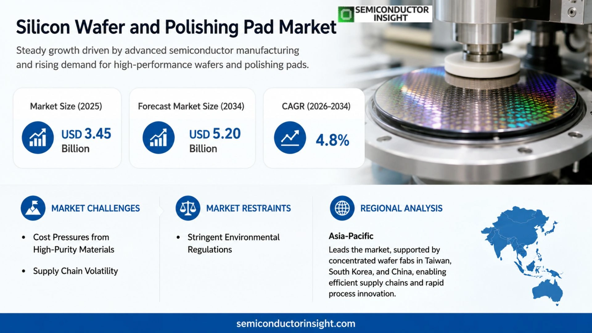
Silicon Wafer and Polishing Pad market size was valued at USD 3.45 billion in 2025. The market will increase from USD 3.60 billion in 2026 to USD 5.20 billion by 2034, exhibiting a CAGR of 4.8% during the forecast period.
Silicon wafers and polishing pads are specialized materials used during the planarization step of semiconductor manufacturing to obtain high smoothness and precise flatness on wafer surfaces.
The sector is expanding because semiconductor devices require ever‑finer geometries, which raises demand for advanced polishing solutions. Moreover, the shift toward high‑performance computing and automotive electronics intensifies the need for reliable wafer finishing processes. Recent collaborations among leading material suppliers aim to introduce low‑defectivity pads that support higher throughput while maintaining surface integrity.
MARKET DRIVERS
Rising Demand for Advanced Semiconductor Nodes
The proliferation of high‑performance computing, AI accelerators and 5G infrastructure is pushing fabs toward sub‑10 nm logic and heterogeneous integration. These cutting‑edge nodes rely on larger‑diameter silicon wafers,primarily 300 mm and an emerging 450 mm cohort,because a single wafer yields more dies, driving economies of scale. To achieve the required surface planarity, manufacturers depend on precision polishing pads that can consistently deliver sub‑nanometer roughness. Consequently, Silicon Wafer and Polishing Pad Market volumes are expanding in lockstep with node advancement.
Shift Toward Sustainable Manufacturing Practices
Regulatory bodies and OEMs alike are rewarding fabs that reduce chemical waste and energy intensity. Modern polishing pads formulated from biodegradable polymers or reclaimed materials enable lower slurry consumption and fewer hazardous by‑products. Companies that embed these green attributes into their product line are seeing faster adoption rates, as end‑users translate sustainability metrics into procurement preferences. This trend is compelling pad suppliers to innovate material science while preserving throughput.
➤ The integration of larger‑diameter wafers directly amplifies pad consumption, reshaping supplier dynamics.
From a commercial standpoint, the twin forces of node scaling and eco‑efficiency are prompting equipment integrators to lock‑in long‑term contracts with pad manufacturers. Firms that can demonstrate consistent defect reduction and lower total cost of ownership are positioned to capture the bulk of upcoming spend, prompting a modest but steady rise in market revenues.
MARKET CHALLENGES
Cost Pressures from High‑Purity Materials
Producing polishing pads that meet the ultra‑low defect thresholds of leading‑edge fabs requires high‑purity silica, specialty elastomers and precisely engineered surface chemistries. The price volatility of these inputs,exacerbated by limited supplier bases,compresses margins for pad vendors, especially those operating on a cost‑plus model. End‑users pass a portion of these expenses downstream, making price negotiations increasingly contentious.
Other Challenges
Supply Chain Volatility
Geopolitical tensions and logistics bottlenecks have introduced unpredictable lead times for raw materials such as high‑grade polymer beads. Manufacturers must now buffer inventory or diversify sourcing, both of which inflate working capital requirements and erode flexibility in responding to rapid technology shifts.
MARKET RESTRAINTS
Stringent Environmental Regulations
Legislation in major semiconductor hubs,particularly in East Asia and Europe,has tightened limits on volatile organic compounds (VOCs) and slurry discharge. Pad manufacturers are compelled to redesign formulations to comply, a process that often demands substantial R&D spend and re‑qualification cycles. The time and cost associated with regulatory approval can delay product roll‑outs, constraining market expansion.
MARKET OPPORTUNITIES
Emergence of 300 mm and 450 mm Wafer Platforms
The migration toward 300 mm and the nascent 450 mm wafer standards unlocks a sizable growth corridor for polishing pads. Larger wafers demand pads with enhanced uniformity and thermal stability, creating a niche for specialized chem‑mechanical solutions. Early entrants that secure intellectual property around high‑temperature elastomers and low‑particle‑generation matrices stand to lock in multi‑year supply agreements, translating technical leadership into sustainable revenue streams.
Silicon Wafer and Polishing Pad Market Trends
Elevated Demand for High‑Precision Polishing Materials
The surge in advanced semiconductor architectures,particularly 5‑nanometer logic chips and power‑dense SiC devices,has heightened the requirement for wafer surfaces that meet tighter flatness tolerances. Manufacturers are turning to more refined polishing pads that can sustain sub‑nanometer roughness while minimizing material removal rates. This shift reflects a broader industry effort to enhance yield margins by reducing defect incidence during the final polishing stage. As fab lines adopt higher‑density interconnects, the cost of rework escalates, prompting a strategic focus on polishing solutions that deliver consistent performance across larger wafer diameters.
Other Trends
Regional Acceleration in Asia‑Pacific
Asia‑Pacific continues to outpace other regions as the primary hub for semiconductor fabrication. Nations such as China, South Korea, and Taiwan have expanded capacity for both silicon and silicon‑carbide wafer production, creating a parallel demand surge for specialized polishing pads. Local suppliers are leveraging proximity to fabs to shorten supply chains and provide customized pad chemistries aligned with regional process variations. This geographic concentration also encourages collaborative R&D initiatives between fab operators and pad manufacturers, accelerating the introduction of next‑generation abrasive technologies that address the thermal and mechanical stresses unique to high‑power devices.
Sustainability and Material Innovation
Environmental considerations are reshaping procurement criteria across Silicon Wafer and Polishing Pad Market. Companies are evaluating pad substrates that incorporate recycled polymers and lower‑emission slurry formulations, aiming to reduce the carbon footprint of wafer polishing cycles. Concurrently, research into nano‑engineered abrasive particles promises to extend pad lifespans, thereby decreasing consumable turnover. For end‑users, these developments translate into operational cost savings and compliance with increasingly stringent regulatory standards on waste management. Firms that integrate sustainability into their product portfolios are positioning themselves as preferred partners for fab operators seeking both performance and environmental stewardship.
COMPETITIVE LANDSCAPE
Key Industry Players
Silicon Wafer and Polishing Pad Market: Competitive Overview
The segment is dominated by a handful of vertically integrated manufacturers that control both wafer growth and polishing consumables. Shin‑Etsu Chemical, Sumco, and GlobalWafers together account for a sizable share of total revenue, leveraging large‑scale crystal pulling capacity and long‑standing relationships with leading fab operators. Their ability to co‑develop polishing pad chemistries that match evolving device geometries gives them a pricing advantage and creates barriers for new entrants. Siltronic and SK Siltron complement the landscape with strong European and Korean footprints, respectively, and they frequently acquire niche technology firms to broaden their pad‑material portfolios. This concentration of scale and R&D depth forces smaller suppliers to specialize in high‑margin niche applications such as silicon‑carbide wafer polishing or ultra‑thin pad formats for advanced logic nodes.
Beyond the tier‑one giants, a diverse set of companies competes on niche performance metrics, regional presence, or differentiated surface‑treatment processes. Ferrotec, ASM International, and Gritek focus on precision tooling and custom pad formulations for memory and analog devices, where surface uniformity drives yield. Chinese players such as Guosheng, QL Electronics, and Zhonghuan have accelerated capacity expansion to serve domestic fab growth, often partnering with local semiconductor alliances. Meanwhile, specialty chemical groups like DuPont, Cabot, and FUJIBO supply abrasive compounds and binding agents that enable thinner, more resilient pads. The competitive pressure generated by these varied business models fuels continuous innovation in slurry chemistry, pad texture engineering, and sustainability initiatives.
List of Key Silicon Wafer and Polishing Pad Companies Profiled
- Shin‑Etsu Chemical
- Sumco
- GlobalWafers
- Siltronic
- SK Siltron
- WaferWorks
- Ferrotec
- ASM International
- Gritek
- Guosheng
- QL Electronics
- MCL
- National Silicon Industry Group
- Poshing
- DuPont
- Cabot
- FUJIBO
Segment Analysis:
| Segment Category | Sub-Segments | Key Insights |
| By Type |
|
Silicon Carbide Wafer is emerging as the preferred type for high‑performance semiconductor nodes because it delivers superior thermal conductivity and mechanical strength.
|
| By Application |
|
Logic and MPU drives demand for ultra‑smooth wafer surfaces, as modern microprocessors require strict critical dimension control.
|
| By End User |
|
Semiconductor Fabricators shape the market trajectory because they integrate wafer polishing directly into high‑volume manufacturing lines.
|
| By Process Stage |
|
CMP remains the core stage where wafer polishing pads and silicon wafers interact intensively.
|
| By Performance Requirement |
|
Ultra‑Flatness is a decisive criterion for next‑generation logic and memory devices, guiding material selection.
|
Regional Analysis: Silicon Wafer and Polishing Pad Market
Asia‑Pacific
Proximity between wafer manufacturers and pad suppliers shortens material transit, allowing rapid feedback loops on pad performance. This logistical edge supports just‑in‑time inventory practices and diminishes risk of stockouts during peak fab cycles.
OEMs and pad producers frequently engage in co‑engineering projects, aligning pad texture and chemistry with next‑generation lithography requirements. Such collaborations accelerate time‑to‑market for advanced node wafers.
Regional environmental standards prioritize low‑waste polishing processes. Companies that embed recyclable pad materials gain regulatory goodwill and lower compliance costs, reinforcing their market position.
A deep pool of process engineers and materials scientists in the area fuels continuous innovation in pad formulation, ensuring that the region remains at the forefront of surface‑finishing technology.
North America
North America maintains a sophisticated ecosystem of research institutions and high‑value fab facilities, especially in the United States. The market here is shaped by a strong emphasis on reliability and yield enhancement, prompting customers to adopt premium polishing pads that deliver consistent surface uniformity. Strategic investments by major semiconductor producers in advanced packaging have spurred niche demand for specialty pads compatible with heterogeneous integration. While the overall volume may lag behind Asia‑Pacific, contract manufacturers in this region leverage differentiated services,such as real‑time pad wear monitoring,to command higher price points. The competitive pressure encourages ongoing refinement of pad texture, reinforcing the region’s reputation for quality‑driven solutions.
Europe
European players benefit from a mature industrial base and stringent quality standards that influence purchasing decisions across Silicon Wafer and Polishing Pad Market. The continent’s emphasis on circular economy principles drives a gradual shift toward reusable pad technologies, encouraging collaborations between chemical firms and equipment makers. Nations with strong semiconductor roadmaps, such as Germany and the Netherlands, invest heavily in R&D to align pad performance with emerging EUV lithography processes. Although the total addressable market is modest, the focus on precision engineering makes Europe an incubator for high‑efficiency pad designs that often find export pathways to other regions.
South America
South America’s involvement in Silicon Wafer and Polishing Pad Market remains nascent, yet growing interest is observable in Brazil and Chile where pilot fabs are exploring niche specialty nodes. Market participants here prioritize cost‑effective polishing solutions that balance performance with the region’s price‑sensitive manufacturing environment. Local distributors are beginning to offer value‑added services, such as on‑site pad conditioning, to mitigate logistics constraints. As regional governments outline incentives for semiconductor assembly, the demand for reliable polishing consumables is expected to gain traction, creating entry points for multinational suppliers.
Middle East & Africa
The Middle East & Africa region showcases a fragmented landscape, with emerging fabrication hubs in the United Arab Emirates and nascent projects in South Africa. Demand is primarily driven by government‑led initiatives aiming to diversify economies through high‑tech manufacturing. Clients in these markets seek robust polishing pads that can endure harsher ambient conditions while delivering the surface flatness required for advanced node production. Partnerships with established Asian pad manufacturers are becoming common, allowing local fabs to import proven technologies while developing in‑house expertise. Although volume remains limited, the strategic intent signals a long‑term growth horizon for Silicon Wafer and Polishing Pad Market in this geography.
Report Scope
This market research report provides a comprehensive analysis of the Silicon Wafer and Polishing Pad Market , covering the forecast period 2026–2034. It offers detailed insights into market dynamics, technological advancements, competitive landscape, and key trends shaping the industry.
Key focus areas of the report include:
- Market Size & Forecast: Historical data and future projections for revenue, unit shipments, and market value across major regions and segments.
- Segmentation Analysis: Detailed breakdown by product type, technology, application, and end-user industry to identify high-growth segments and investment opportunities.
- Regional Insights: Insights into market performance across North America, Europe, Asia-Pacific, Latin America, and the Middle East & Africa, including country-level analysis where relevant.
- Competitive Landscape: Profiles of leading market participants, including their product offerings, R&D focus, manufacturing capacity, pricing strategies, and recent developments such as mergers, acquisitions, and partnerships.
- Technology Trends & Innovation: Assessment of emerging technologies, integration of AI/IoT, semiconductor design trends, fabrication techniques, and evolving industry standards.
- Market Drivers & Restraints: Evaluation of factors driving market growth along with challenges, supply chain constraints, regulatory issues, and market-entry barriers.
- Stakeholder Insights: Insights for component suppliers, OEMs, system integrators, investors, and policymakers regarding the evolving ecosystem and strategic opportunities.
Primary and secondary research methods are employed, including interviews with industry experts, data from verified sources, and real-time market intelligence to ensure the accuracy and reliability of the insights presented.
FREQUENTLY ASKED QUESTIONS:
What is the current market size of Silicon Wafer and Polishing Pad Market?
-> Global Silicon Wafer and Polishing Pad market will increase from USD 3.60 billion in 2026 to USD 5.20 billion by 2034, exhibiting a CAGR of 4.8%
Which key companies operate in Silicon Wafer and Polishing Pad Market?
-> Key players include Shin‑Etsu Chemical, Sumco, Global Wafers, Siltronic, SK siltron, Waferworks, Ferrotec, AST, Gritek, Guosheng, QL Electronics, MCL, National Silicon Industry Group, Poshing, Zhonghuan, DuPont, Cabot, FUJIBO, among others.
What are the key growth drivers?
-> Key growth drivers include rising demand for silicon wafers in memory, logic, analog and sensor applications; the critical role of wafer polishing for device performance; and the push for higher yield and lower defect densities in semiconductor manufacturing.
Which region dominates the market?
-> Asia leads the market, driven by strong semiconductor manufacturing bases in China, Japan, South Korea and Taiwan, while North America and Europe also hold significant shares.
What are the emerging trends?
-> Emerging trends include adoption of silicon carbide wafers, development of next‑generation polishing pads with enhanced durability, integration of AI‑driven process control, and sustainability initiatives targeting lower chemical usage and waste reduction.

Get Sample Report PDF for Exclusive Insights
Report Sample Includes
- Table of Contents
- List of Tables & Figures
- Charts, Research Methodology, and more...
 Download Sample Report PDF