Semiconductor Wafer Dry Etching Equipment Market Overview
Semiconductor wafer dry etching equipment is a type of manufacturing tool used in the semiconductor industry for the process of etching or removing material from the surface of semiconductor wafers. Etching is a critical step in semiconductor device fabrication, allowing precise patterning of features on the wafer surface. Dry etching, as opposed to wet etching, involves using plasma or reactive gases to chemically or physically remove material from the wafer surface.
This report provides a deep insight into the global Semiconductor Wafer Dry Etching Equipment market covering all its essential aspects. This ranges from a macro overview of the market to micro details of the market size, competitive landscape, development trend, niche market, key market drivers and challenges, SWOT analysis, value chain analysis, etc.
The analysis helps the reader to shape the competition within the industries and strategies for the competitive environment to enhance the potential profit. Furthermore, it provides a simple framework for evaluating and accessing the position of the business organization. The report structure also focuses on the competitive landscape of the Global Semiconductor Wafer Dry Etching Equipment Market, this report introduces in detail the market share, market performance, product situation, operation situation, etc. of the main players, which helps the readers in the industry to identify the main competitors and deeply understand the competition pattern of the market.
In a word, this report is a must-read for industry players, investors, researchers, consultants, business strategists, and all those who have any kind of stake or are planning to foray into the Semiconductor Wafer Dry Etching Equipment market in any manner.
Semiconductor Wafer Dry Etching Equipment Market Analysis:
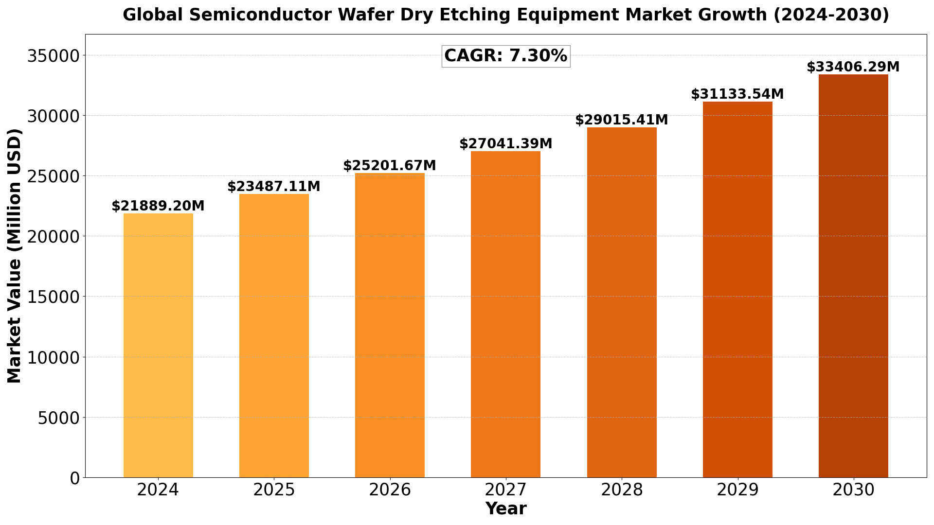
The Global Semiconductor Wafer Dry Etching Equipment Market size was estimated at USD 20400 million in 2023 and is projected to reach USD 33406.29 million by 2030, exhibiting a CAGR of 7.30% during the forecast period.
North America Semiconductor Wafer Dry Etching Equipment market size was USD 5315.66 million in 2023, at a CAGR of 6.26% during the forecast period of 2024 through 2030.
Semiconductor Wafer Dry Etching Equipment Key Market Trends :
- Growing Demand for Advanced Semiconductor Devices: As semiconductor technology continues to evolve, the demand for smaller, more powerful chips for applications in 5G, AI, IoT, automotive, and high-performance computing is accelerating. Dry etching is crucial in the fabrication of these devices, particularly for creating intricate circuit patterns at smaller nodes (e.g., 5nm, 3nm). The increasing complexity and miniaturization of semiconductor devices is driving demand for advanced dry etching equipment.
- Technological Advancements in Dry Etching Techniques: Innovations in dry etching technologies, such as reactive ion etching (RIE), inductively coupled plasma (ICP) etching, and atomic layer etching (ALE), are pushing the boundaries of precision and efficiency. These advancements enable semiconductor manufacturers to achieve the high resolution and uniformity required for next-generation chips, making dry etching equipment more sophisticated and in-demand.
- Increase in Semiconductor Manufacturing Capacity: As the global semiconductor market continues to grow, there is a rising need for new and upgraded fabrication plants (fabs). The expansion of manufacturing capacity in regions like Asia-Pacific, North America, and Europe is boosting demand for dry etching equipment. The growing number of fabs dedicated to producing advanced semiconductors further fuels the need for efficient, high-performance etching systems.
- Focus on Yield Improvement and Cost Efficiency: Semiconductor manufacturers are increasingly focusing on improving yields and reducing defects during the production process. Dry etching plays a key role in achieving precise etching and patterning of wafers, which is essential for ensuring high yields. Manufacturers are adopting advanced dry etching equipment to minimize defects, improve process control, and enhance the overall efficiency of semiconductor fabrication.
- Sustainability and Environmental Considerations: As environmental regulations and sustainability become more prominent, the semiconductor industry is adopting cleaner and more energy-efficient processes. Modern dry etching equipment is being designed with a focus on reducing energy consumption, waste, and harmful chemical emissions. These more eco-friendly solutions are appealing to semiconductor manufacturers looking to comply with increasingly stringent environmental standards.
Semiconductor Wafer Dry Etching Equipment Market Regional Analysis :

1. North America (USA, Canada, Mexico)
- USA: The largest market in the region due to advanced infrastructure, high disposable income, and technological advancements. Key industries include technology, healthcare, and manufacturing.
- Canada: Strong market potential driven by resource exports, a stable economy, and government initiatives supporting innovation.
- Mexico: A growing economy with strengths in automotive manufacturing, agriculture, and tourism, benefitting from trade agreements like the USMCA.
2. Europe (Germany, UK, France, Russia, Italy, Rest of Europe)
- Germany: The region’s industrial powerhouse with a focus on engineering, automotive, and machinery.
- UK: A hub for financial services, fintech, and pharmaceuticals, though Brexit has altered trade patterns.
- France: Strong in luxury goods, agriculture, and aerospace with significant innovation in renewable energy.
- Russia: Resource-driven economy with strengths in oil, gas, and minerals but geopolitical tensions affect growth.
- Italy: Known for fashion, design, and manufacturing, especially in luxury segments.
- Rest of Europe: Includes smaller yet significant economies like Spain, Netherlands, and Switzerland with strengths in finance, agriculture, and manufacturing.
3. Asia-Pacific (China, Japan, South Korea, India, Southeast Asia, Rest of Asia-Pacific)
- China: The largest market in the region with a focus on technology, manufacturing, and e-commerce. Rapid urbanization and middle-class growth fuel consumption.
- Japan: Technological innovation, particularly in robotics and electronics, drives the economy.
- South Korea: Known for technology, especially in semiconductors and consumer electronics.
- India: Rapidly growing economy with strengths in IT services, agriculture, and pharmaceuticals.
- Southeast Asia: Key markets like Indonesia, Thailand, and Vietnam show growth in manufacturing and tourism.
- Rest of Asia-Pacific: Emerging markets with growing investment in infrastructure and services.
4. South America (Brazil, Argentina, Colombia, Rest of South America)
- Brazil: Largest economy in the region, driven by agriculture, mining, and energy.
- Argentina: Known for agriculture exports and natural resources but faces economic instability.
- Colombia: Growing economy with strengths in oil, coffee, and flowers.
- Rest of South America: Includes Chile and Peru, which have strong mining sectors.
5. The Middle East and Africa (Saudi Arabia, UAE, Egypt, Nigeria, South Africa, Rest of MEA)
- Saudi Arabia: Oil-driven economy undergoing diversification with Vision 2030 initiatives.
- UAE: Financial hub with strengths in tourism, real estate, and trade.
- Egypt: Growing infrastructure development and tourism.
- Nigeria: Largest economy in Africa with strengths in oil and agriculture.
- South Africa: Industrialized economy with strengths in mining and finance.
- Rest of MEA: Includes smaller yet resource-rich markets like Qatar and Kenya with growing infrastructure investments.
Semiconductor Wafer Dry Etching Equipment Market Segmentation :
The research report includes specific segments by region (country), manufacturers, Type, and Application. Market segmentation creates subsets of a market based on product type, end-user or application, Geographic, and other factors. By understanding the market segments, the decision-maker can leverage this targeting in the product, sales, and marketing strategies. Market segments can power your product development cycles by informing how you create product offerings for different segments.
Key Company
- Lam Research
- Tokyo Electron Limited
- Applied Materials
- Hitachi High-Tech
- SEMES
- AMEC
- NAURA
- SPTS Technologies (KLA)
- Oxford Instruments
- ULVAC
- Plasma-Therm
- Inductively Coupled Plasma (ICP)
- Capacitive Coupled Plasma (CCP)
- Reactive Ion Etching (RIE)
- Deep Reactive Ion Etching (DRIE)
- Others
- 300 mm Wafer
- 200 mm Wafer
- Others
Drivers
- Miniaturization of Semiconductor Devices: As the demand for smaller and more powerful semiconductor devices increases, dry etching technology becomes essential. The trend toward smaller process nodes (e.g., 5nm, 3nm) requires precise etching capabilities that dry etching equipment offers. These smaller nodes demand greater accuracy and precision in etching, driving the demand for advanced dry etching systems.
- Increase in Demand for Advanced Chips: The rise in demand for high-performance semiconductor chips used in smartphones, AI, data centers, IoT, and automotive applications is propelling the growth of the wafer dry etching market. These chips require extremely fine patterns and structures, which can only be achieved through advanced etching technologies like dry etching.
- Advancements in 5G and Telecommunications: The growing roll-out of 5G networks, and the increasing demand for connected devices and infrastructure, is pushing the need for higher-performance semiconductor devices. This requires dry etching technologies to produce the intricate features on chips used in these applications.
- Expansion of Semiconductor Manufacturing Facilities (Fabs): As semiconductor manufacturing expands, particularly in regions such as China, India, and Southeast Asia, the demand for dry etching equipment is growing. The proliferation of new semiconductor fabs and the upgrade of existing facilities for more advanced chip production is a key driver of market growth.
- Rise of Electric Vehicles (EVs) and Autonomous Vehicles: The automotive sector’s adoption of semiconductor-based technologies, such as those used in electric powertrains, ADAS (advanced driver-assistance systems), and autonomous vehicles, is fueling the demand for high-performance semiconductors, thereby driving the need for precision dry etching equipment.
- Demand for MEMS and Sensors: The increased use of MEMS (Microelectromechanical Systems) and sensors in various industries, including consumer electronics, automotive, healthcare, and aerospace, is driving the demand for dry etching equipment. These devices require extremely fine patterning, which is facilitated by dry etching technologies.
Restraints
- High Initial Capital Investment: Semiconductor wafer dry etching equipment can be very expensive, especially advanced systems capable of handling smaller nodes and complex semiconductor processes. The high initial cost of purchasing and installing this equipment can be a barrier for smaller semiconductor manufacturers and startups.
- Maintenance and Operational Costs: Dry etching equipment requires regular maintenance and servicing to ensure high-performance standards and minimize downtime. The cost of spare parts, replacement consumables, and technician support can add to the operational costs for semiconductor manufacturers.
- Complexity of Process Control: The dry etching process requires precise control over gas flow, pressure, temperature, and other parameters. Maintaining the consistency and repeatability of the etching process can be challenging, and even small deviations can lead to defects in semiconductor devices.
- Supply Chain Challenges: The semiconductor industry has faced supply chain disruptions in recent years, which can impact the availability of components and materials needed for dry etching equipment. This includes the supply of specialized gases, components, and materials used in the etching process, which can delay production and increase costs.
- Environmental and Safety Regulations: The use of reactive gases and chemicals in dry etching processes can pose environmental and safety risks. Stringent regulations regarding the handling, storage, and disposal of these materials may add complexity to the operation of dry etching equipment, driving up compliance costs.
Opportunities
- Innovation in Dry Etching Technologies: There are significant opportunities for companies to innovate in the dry etching space. This includes developing new etching techniques such as atomic layer etching (ALE) and advancements in plasma etching to achieve even finer features and higher precision. Innovation in these areas will cater to the growing needs of smaller semiconductor nodes (e.g., 5nm, 3nm, etc.).
- Development of Eco-Friendly Etching Processes: As the semiconductor industry faces increased environmental pressure, there is a growing demand for eco-friendly dry etching technologies that minimize harmful emissions and chemical waste. Developing sustainable etching solutions that are both effective and environmentally friendly presents an opportunity for market growth.
- Expansion of 5G Networks: The ongoing rollout of 5G infrastructure creates opportunities for the dry etching equipment market. The need for advanced chips in 5G infrastructure equipment, smartphones, and other devices will drive demand for high-precision dry etching equipment capable of producing advanced semiconductor components.
- Adoption of Advanced Packaging Technologies: Advanced semiconductor packaging techniques such as 3D packaging, fan-out wafer-level packaging (FOWLP), and system-in-package (SiP) require precise etching to ensure the effective integration of multiple components. The growing demand for these packaging technologies presents a significant opportunity for dry etching equipment manufacturers.
- Increase in Semiconductor Research and Development (R&D): As semiconductor technology continues to evolve, research and development activities to discover new materials, architectures, and processes will drive the need for cutting-edge dry etching equipment. Semiconductor R&D labs and universities are increasingly looking for advanced etching tools to support the development of next-generation chips.
- Rising Demand for IoT and Smart Devices: The growing demand for Internet of Things (IoT) devices and smart electronics presents a unique opportunity for the dry etching market. These devices require tiny, highly integrated semiconductor components, making advanced etching techniques essential.
Challenges
- Increasing Pressure on Performance and Yield: As semiconductor nodes shrink, achieving high performance and yield becomes increasingly difficult. The challenge for dry etching equipment manufacturers is to provide solutions that can meet the stringent requirements for precision while maintaining high yield and low defect rates.
- Intense Competition in the Market: The semiconductor wafer dry etching equipment market is highly competitive, with several players offering similar products. Leading companies must continually invest in R&D to stay ahead of the competition and develop new technologies to meet the increasing demands of the semiconductor industry.
- Shortage of Skilled Workforce: Operating and maintaining advanced dry etching equipment requires a highly skilled workforce. The shortage of qualified technicians and engineers who can manage and maintain these complex systems poses a challenge for semiconductor manufacturers, especially in emerging markets.
- Economic Volatility: The semiconductor market is vulnerable to global economic cycles. Economic downturns or recessions can impact the capital investment budgets of semiconductor companies, leading to delayed or reduced purchasing of new dry etching equipment.
- Complex Integration with Other Manufacturing Systems: Dry etching equipment must be integrated with other semiconductor fabrication processes, such as deposition, cleaning, and photolithography. Ensuring that the etching equipment works seamlessly within an integrated manufacturing line requires advanced engineering and customization, which can be challenging.
Key Benefits of This Market Research:
- Industry drivers, restraints, and opportunities covered in the study
- Neutral perspective on the market performance
- Recent industry trends and developments
- Competitive landscape & strategies of key players
- Potential & niche segments and regions exhibiting promising growth covered
- Historical, current, and projected market size, in terms of value
- In-depth analysis of the Semiconductor Wafer Dry Etching Equipment Market
- Overview of the regional outlook of the Semiconductor Wafer Dry Etching Equipment Market:
Key Reasons to Buy this Report:
- Access to date statistics compiled by our researchers. These provide you with historical and forecast data, which is analyzed to tell you why your market is set to change
- This enables you to anticipate market changes to remain ahead of your competitors
- You will be able to copy data from the Excel spreadsheet straight into your marketing plans, business presentations, or other strategic documents
- The concise analysis, clear graph, and table format will enable you to pinpoint the information you require quickly
- Provision of market value (USD Billion) data for each segment and sub-segment
- Indicates the region and segment that is expected to witness the fastest growth as well as to dominate the market
- Analysis by geography highlighting the consumption of the product/service in the region as well as indicating the factors that are affecting the market within each region
- Competitive landscape which incorporates the market ranking of the major players, along with new service/product launches, partnerships, business expansions, and acquisitions in the past five years of companies profiled
- Extensive company profiles comprising of company overview, company insights, product benchmarking, and SWOT analysis for the major market players
- The current as well as the future market outlook of the industry concerning recent developments which involve growth opportunities and drivers as well as challenges and restraints of both emerging as well as developed regions
- Includes in-depth analysis of the market from various perspectives through Porters five forces analysis
- Provides insight into the market through Value Chain
- Market dynamics scenario, along with growth opportunities of the market in the years to come
- 6-month post-sales analyst support
Customization of the Report
In case of any queries or customization requirements, please connect with our sales team, who will ensure that your requirements are met.
FAQs
Q1. What is Semiconductor Wafer Dry Etching Equipment?
A1. Semiconductor wafer dry etching equipment is used in the semiconductor manufacturing process to etch or pattern wafer surfaces using reactive gases, enabling the creation of precise features on semiconductor devices.
Q2. What is the current market size and forecast for the Semiconductor Wafer Dry Etching Equipment market until 2030?
A2. The market size was estimated at USD 20400 million in 2023 and is projected to reach USD 33406.29 million by 2030, exhibiting a CAGR of 7.30% during the forecast period.
Q3. What are the key growth drivers in the Semiconductor Wafer Dry Etching Equipment market?
A3. Key growth drivers include the increasing demand for smaller and more complex semiconductor devices, advancements in etching technology, and the expansion of semiconductor applications in areas like 5G, AI, and IoT.
Q4. Which regions dominate the Semiconductor Wafer Dry Etching Equipment market?
A4. The Asia-Pacific region, particularly China, South Korea, and Japan, dominates the market due to their strong semiconductor manufacturing industries and high demand for advanced etching equipment.
Q5. What are the emerging trends in the Semiconductor Wafer Dry Etching Equipment market?
A5. Emerging trends include the development of more precise and efficient etching technologies, the integration of AI for process optimization, and the demand for eco-friendly etching solutions with reduced environmental impact.

Get Sample Report PDF for Exclusive Insights
Report Sample Includes
- Table of Contents
- List of Tables & Figures
- Charts, Research Methodology, and more...