Semiconductor IC Photomask Market Overview
Semiconductor IC Photomasks are high-purity quartz or glass plates that contain a pattern of ICs. These are used in the reproduction of pattern structures for manufacturing printed circuit boards, electronic circuits, and LCD displays, and for the serial production of reticles and other microstructures. Semiconductor Photomasks are used at wavelengths of 365 nm, 248 nm, and 193 nm. ICs are manufactured layer by layer, where each layer requires a unique Semiconductor Photomask. As current generation ICs typically have 25-60 layers, the manufacturing process of Semiconductor Photomasks has become complex.
This report provides a deep insight into the global Semiconductor IC Photomask market covering all its essential aspects. This ranges from a macro overview of the market to micro details of the market size, competitive landscape, development trend, niche market, key market drivers and challenges, SWOT analysis, value chain analysis, etc.
The analysis helps the reader to shape the competition within the industries and strategies for the competitive environment to enhance the potential profit. Furthermore, it provides a simple framework for evaluating and accessing the position of the business organization. The report structure also focuses on the competitive landscape of the Global Semiconductor IC Photomask Market, this report introduces in detail the market share, market performance, product situation, operation situation, etc. of the main players, which helps the readers in the industry to identify the main competitors and deeply understand the competition pattern of the market.
In a word, this report is a must-read for industry players, investors, researchers, consultants, business strategists, and all those who have any kind of stake or are planning to foray into the Semiconductor IC Photomask market in any manner.
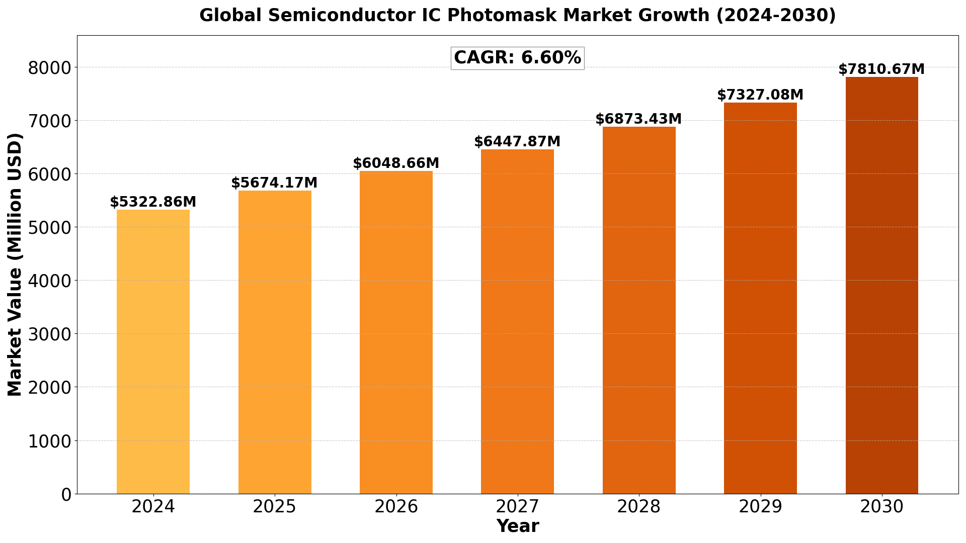
Semiconductor IC Photomask Market Analysis:
The Global Semiconductor IC Photomask Market size was estimated at USD 4993.30 million in 2023 and is projected to reach USD 7810.67 million by 2030, exhibiting a CAGR of 6.60% during the forecast period.
North America Semiconductor IC Photomask market size was USD 1301.11 million in 2023, at a CAGR of 5.66% during the forecast period of 2024 through 2030.
Semiconductor IC Photomask Key Market Trends :
1. Advancements in Semiconductor Manufacturing Technologies
As semiconductor manufacturers move towards smaller process nodes (such as 5nm, 3nm, and even 2nm), the demand for high-quality photomasks is increasing. These advanced nodes require more precise and intricate patterns on the photomasks to ensure the accuracy of chip production. The need for photomasks capable of handling complex designs, including multi-patterning and extreme ultraviolet (EUV) lithography, is driving innovations and growth in the semiconductor IC photomask market.
2. Rise of AI, 5G, and IoT Applications
The increasing adoption of artificial intelligence (AI), 5G technologies, and the Internet of Things (IoT) is contributing to the growing demand for semiconductor chips that are more powerful, energy-efficient, and smaller in size. These applications require advanced integrated circuits that utilize photomasks for precise patterning during manufacturing. As demand for AI chips, 5G infrastructure, and IoT devices grows, photomask manufacturers are expected to see increased demand for their products to support these advanced semiconductor designs.
3. Increased Use of EUV Lithography
Extreme Ultraviolet (EUV) lithography is becoming an essential technology for advanced semiconductor manufacturing, especially for process nodes below 7nm. EUV lithography requires highly accurate photomasks to create fine features on silicon wafers. As semiconductor companies transition to EUV-based processes for manufacturing cutting-edge chips, the demand for EUV photomasks is expected to rise significantly. This trend is particularly evident in the production of logic chips, memory devices, and other high-performance semiconductors used in mobile, automotive, and cloud computing applications.
4. Demand for Advanced Packaging Solutions
With the increasing complexity of semiconductor devices, there is a growing focus on advanced packaging techniques like 3D stacking and system-in-package (SiP) solutions. These innovations require precise photomasks for the production of multi-layered ICs and stacked chip configurations. As semiconductor packaging becomes more advanced, the demand for high-quality photomasks to support these technologies will continue to rise, contributing to market growth.
5. Geopolitical and Supply Chain Considerations
The semiconductor industry is being influenced by ongoing geopolitical tensions and supply chain challenges. This has led to increased investments in semiconductor manufacturing capacity, particularly in regions such as North America, Europe, and Southeast Asia. As more countries focus on building domestic semiconductor fabrication facilities, the demand for photomasks, which are critical components in chip production, is expected to increase. This trend is further amplified by the need for greater self-sufficiency in semiconductor manufacturing to reduce dependency on external sources.
Semiconductor IC Photomask Market Regional Analysis :

1. North America (USA, Canada, Mexico)
- USA: The largest market in the region due to advanced infrastructure, high disposable income, and technological advancements. Key industries include technology, healthcare, and manufacturing.
- Canada: Strong market potential driven by resource exports, a stable economy, and government initiatives supporting innovation.
- Mexico: A growing economy with strengths in automotive manufacturing, agriculture, and tourism, benefitting from trade agreements like the USMCA.
2. Europe (Germany, UK, France, Russia, Italy, Rest of Europe)
- Germany: The region’s industrial powerhouse with a focus on engineering, automotive, and machinery.
- UK: A hub for financial services, fintech, and pharmaceuticals, though Brexit has altered trade patterns.
- France: Strong in luxury goods, agriculture, and aerospace with significant innovation in renewable energy.
- Russia: Resource-driven economy with strengths in oil, gas, and minerals but geopolitical tensions affect growth.
- Italy: Known for fashion, design, and manufacturing, especially in luxury segments.
- Rest of Europe: Includes smaller yet significant economies like Spain, Netherlands, and Switzerland with strengths in finance, agriculture, and manufacturing.
3. Asia-Pacific (China, Japan, South Korea, India, Southeast Asia, Rest of Asia-Pacific)
- China: The largest market in the region with a focus on technology, manufacturing, and e-commerce. Rapid urbanization and middle-class growth fuel consumption.
- Japan: Technological innovation, particularly in robotics and electronics, drives the economy.
- South Korea: Known for technology, especially in semiconductors and consumer electronics.
- India: Rapidly growing economy with strengths in IT services, agriculture, and pharmaceuticals.
- Southeast Asia: Key markets like Indonesia, Thailand, and Vietnam show growth in manufacturing and tourism.
- Rest of Asia-Pacific: Emerging markets with growing investment in infrastructure and services.
4. South America (Brazil, Argentina, Colombia, Rest of South America)
- Brazil: Largest economy in the region, driven by agriculture, mining, and energy.
- Argentina: Known for agriculture exports and natural resources but faces economic instability.
- Colombia: Growing economy with strengths in oil, coffee, and flowers.
- Rest of South America: Includes Chile and Peru, which have strong mining sectors.
5. The Middle East and Africa (Saudi Arabia, UAE, Egypt, Nigeria, South Africa, Rest of MEA)
- Saudi Arabia: Oil-driven economy undergoing diversification with Vision 2030 initiatives.
- UAE: Financial hub with strengths in tourism, real estate, and trade.
- Egypt: Growing infrastructure development and tourism.
- Nigeria: Largest economy in Africa with strengths in oil and agriculture.
- South Africa: Industrialized economy with strengths in mining and finance.
- Rest of MEA: Includes smaller yet resource-rich markets like Qatar and Kenya with growing infrastructure investments.
Semiconductor IC Photomask Market Segmentation :
The research report includes specific segments by region (country), manufacturers, Type, and Application. Market segmentation creates subsets of a market based on product type, end-user or application, Geographic, and other factors. By understanding the market segments, the decision-maker can leverage this targeting in the product, sales, and marketing strategies. Market segments can power your product development cycles by informing how you create product offerings for different segments.
Key Company
- Photronics
- Toppan
- DNP
- Hoya
- ShenZheng QingVi
- Taiwan Mask
- Nippon Filcon
- Compugraphics
- Newway Semiconductor Photomask
Market Segmentation (by Type)
- Quartz Mask
- Soda Mask
Market Segmentation (by Application)
- IC Manufacturing
- IC Packaging and Testing
- Semiconductor Device
- LED Chip
Drivers:
- Growth in Semiconductor Demand: As the demand for semiconductor devices continues to rise across various industries, including consumer electronics, automotive, telecommunications, and data centers, the need for ICs with higher performance and smaller form factors drives the demand for advanced photomasks. The increasing complexity of semiconductor designs requires photomasks with finer and more precise patterns to manufacture smaller, faster, and more efficient ICs.
- Advancements in Semiconductor Fabrication Technology: Technological innovations in semiconductor fabrication, such as extreme ultraviolet (EUV) lithography, have increased the demand for more advanced photomasks. EUV lithography requires photomasks with extremely fine features that can achieve high-resolution patterning, driving the need for specialized, high-quality photomasks to meet the needs of the most advanced semiconductor manufacturing processes.
- Miniaturization of Semiconductor Devices: The continued trend toward miniaturization in semiconductor devices has led to the production of smaller transistors and tighter circuit designs. These designs require photomasks capable of defining increasingly smaller features on semiconductor wafers. As semiconductor manufacturers move towards the 5nm and 3nm process nodes, the demand for high-precision photomasks that can handle these intricate designs continues to grow.
- Increase in 5G, IoT, and AI Technologies: The rapid development and deployment of 5G technology, the expansion of the Internet of Things (IoT), and the rise of artificial intelligence (AI) applications are driving the demand for advanced semiconductors. These applications require high-performance ICs with sophisticated designs, which in turn create a need for advanced photomasks capable of supporting these high-performance requirements.
- Rising Demand for Automotive Semiconductors: The automotive industry is increasingly relying on semiconductors for applications such as autonomous driving, electric vehicles (EVs), infotainment systems, and advanced driver-assistance systems (ADAS). The demand for more complex and reliable automotive ICs has a direct impact on the semiconductor photomask market, as automotive applications require high-quality photomasks to ensure performance, reliability, and safety.
Restraints:
- High Production Costs: The production of semiconductor IC photomasks is an expensive process. The costs involved in manufacturing photomasks, including high-end lithography tools, mask blanks, and the photomask itself, can be prohibitively high, especially as the resolution required for advanced nodes increases. These high costs can deter smaller companies from entering the market and may limit the growth potential for some semiconductor manufacturers.
- Complexity of Manufacturing: As semiconductor process nodes shrink, photomasks need to meet increasingly stringent requirements for precision and accuracy. This complexity in the production process can result in longer lead times, higher manufacturing costs, and an increased risk of defects. Maintaining the required level of quality in photomask production is a challenge for manufacturers, especially as the designs become more intricate and the feature sizes continue to shrink.
- Vulnerability to Supply Chain Disruptions: The semiconductor industry, including the photomask market, is highly dependent on global supply chains for raw materials and specialized equipment. Supply chain disruptions, such as those caused by geopolitical tensions or natural disasters, can lead to delays in the production and delivery of photomasks, which can impact semiconductor manufacturing timelines and costs.
- Competition from Alternative Lithography Techniques: As the semiconductor industry looks for ways to continue shrinking transistor sizes, alternative lithography techniques such as nanoimprint lithography (NIL) and directed self-assembly (DSA) are being explored as potential solutions. These alternative technologies may pose a threat to traditional photomask-based photolithography, as they offer different methods for patterning semiconductor devices and may reduce the reliance on photomasks in the future.
Opportunities:
- Advancements in EUV Lithography: The adoption of extreme ultraviolet (EUV) lithography is a key opportunity for the photomask market. EUV is capable of printing smaller features on semiconductor wafers, enabling the production of ICs at process nodes as small as 7nm, 5nm, and even 3nm. As semiconductor manufacturers continue to transition to EUV lithography for advanced IC production, the demand for high-quality photomasks designed specifically for EUV applications is expected to increase.
- Expansion of the Semiconductor Industry in Emerging Markets: As the global semiconductor industry expands, emerging markets such as China, India, and Southeast Asia are seeing increased investments in semiconductor manufacturing. These regions are likely to drive demand for semiconductor IC photomasks as they develop their local semiconductor production capabilities. Localizing photomask production and supply chains in these markets presents a growth opportunity for photomask suppliers.
- Innovations in Photomask Materials and Coatings: The development of new materials and coatings for photomasks, such as advanced mask blanks and anti-reflective coatings, presents opportunities to enhance the performance and efficiency of photomasks. Innovations in photomask materials could reduce defects, improve resolution, and lower production costs, driving further demand for advanced semiconductor IC photomasks.
- Growing Demand for Specialized Photomasks: As semiconductor applications become more diverse, there is a growing need for specialized photomasks designed for specific use cases. For instance, photomasks for power semiconductors, automotive ICs, and sensors may have different requirements than those used for general-purpose ICs. This demand for specialized photomasks offers manufacturers an opportunity to cater to niche markets and develop customized solutions.
- Development of Advanced Metrology Techniques: As the photomask market advances, the need for accurate measurement and inspection of photomasks becomes more critical. The development of advanced metrology techniques for characterizing photomasks, including mask pattern fidelity and defect detection, offers significant opportunities for companies that provide photomask inspection and quality assurance services.
Challenges:
- Complexity of Defect Inspection and Repair: As the semiconductor process nodes shrink, the complexity of detecting and repairing defects in photomasks becomes more challenging. At smaller nodes, even minor defects in photomasks can lead to significant yield loss in semiconductor manufacturing. The increasing difficulty in defect inspection and repair at smaller nodes presents a major challenge for the industry.
- Technological Barriers to Advancing Lithography: Achieving smaller node sizes in semiconductor manufacturing requires advancing lithography techniques, which includes the development of photomasks with ever-finer patterns. However, there are technological barriers to continuing to shrink transistor sizes, including challenges related to resolution, patterning fidelity, and optical effects. Overcoming these barriers will require significant investments in research and development, creating both challenges and opportunities for the photomask market.
- Dependence on a Limited Number of Photomask Suppliers: The photomask market is dominated by a few key players, including companies like Toppan Photomasks and Photronics. This limited number of suppliers could lead to supply chain vulnerabilities and potential price fluctuations. Additionally, any disruptions in the production capabilities of these major players could have a significant impact on semiconductor manufacturing.
- Environmental and Regulatory Challenges: As the photomask industry evolves, there may be increasing pressure to comply with environmental and regulatory standards. The production of photomasks involves the use of hazardous chemicals, and manufacturers must adhere to strict environmental regulations. Ensuring compliance with these standards while maintaining production efficiency could be a challenge for photomask manufacturers.
Key Benefits of This Market Research:
- Industry drivers, restraints, and opportunities covered in the study
- Neutral perspective on the market performance
- Recent industry trends and developments
- Competitive landscape & strategies of key players
- Potential & niche segments and regions exhibiting promising growth covered
- Historical, current, and projected market size, in terms of value
- In-depth analysis of the Semiconductor IC Photomask Market
- Overview of the regional outlook of the Semiconductor IC Photomask Market:
Key Reasons to Buy this Report:
- Access to date statistics compiled by our researchers. These provide you with historical and forecast data, which is analyzed to tell you why your market is set to change
- This enables you to anticipate market changes to remain ahead of your competitors
- You will be able to copy data from the Excel spreadsheet straight into your marketing plans, business presentations, or other strategic documents
- The concise analysis, clear graph, and table format will enable you to pinpoint the information you require quickly
- Provision of market value (USD Billion) data for each segment and sub-segment
- Indicates the region and segment that is expected to witness the fastest growth as well as to dominate the market
- Analysis by geography highlighting the consumption of the product/service in the region as well as indicating the factors that are affecting the market within each region
- Competitive landscape which incorporates the market ranking of the major players, along with new service/product launches, partnerships, business expansions, and acquisitions in the past five years of companies profiled
- Extensive company profiles comprising of company overview, company insights, product benchmarking, and SWOT analysis for the major market players
- The current as well as the future market outlook of the industry concerning recent developments which involve growth opportunities and drivers as well as challenges and restraints of both emerging as well as developed regions
- Includes in-depth analysis of the market from various perspectives through Porters five forces analysis
- Provides insight into the market through Value Chain
- Market dynamics scenario, along with growth opportunities of the market in the years to come
- 6-month post-sales analyst support
Customization of the Report
In case of any queries or customization requirements, please connect with our sales team, who will ensure that your requirements are met.
FAQs
Q1. What is the Semiconductor IC Photomask market?
A1. The Semiconductor IC Photomask market involves the production and sale of photomasks used in semiconductor manufacturing, which are used as templates to transfer circuit patterns onto semiconductor wafers during the photolithography process.
Q2. What is the current market size and forecast for the Semiconductor IC Photomask market until 2030?
A2. The market size was estimated at USD 4,993.30 million in 2023 and is projected to reach USD 7,810.67 million by 2030, exhibiting a CAGR of 6.60% during the forecast period.
Q3. What are the key growth drivers in the Semiconductor IC Photomask market?
A3. Key growth drivers include the increasing demand for advanced semiconductor devices, the rise of miniaturization in ICs, the growth of AI, 5G, and automotive applications, and technological advancements in photomask manufacturing processes.
Q4. Which regions dominate the Semiconductor IC Photomask market?
A4. The Asia-Pacific region, particularly countries like Taiwan, South Korea, and China, dominate the Semiconductor IC Photomask market due to the high concentration of semiconductor manufacturing and advanced lithography technologies in these regions.
Q5. What are the emerging trends in the Semiconductor IC Photomask market?
A5. Emerging trends include the development of photomasks for extreme ultraviolet (EUV) lithography, the increasing demand for photomasks in the production of next-generation semiconductor nodes, and advancements in mask inspection and repair technologies.
Get Sample Report PDF for Exclusive Insights
Report Sample Includes
- Table of Contents
- List of Tables & Figures
- Charts, Research Methodology, and more...


