Semiconductor Defect Automated Inspection System Market Overview
Semiconductor defect automated inspection equipment plays a crucial role in the semiconductor manufacturing process. It is used to detect and identify defects in semiconductor devices or chips, ensuring product quality and performance.
This report provides a deep insight into the global Semiconductor Defect Automated Inspection System market covering all its essential aspects. This ranges from a macro overview of the market to micro details of the market size, competitive landscape, development trend, niche market, key market drivers and challenges, SWOT analysis, value chain analysis, etc.
The analysis helps the reader to shape the competition within the industries and strategies for the competitive environment to enhance the potential profit. Furthermore, it provides a simple framework for evaluating and accessing the position of the business organization. The report structure also focuses on the competitive landscape of the Global Semiconductor Defect Automated Inspection System Market, this report introduces in detail the market share, market performance, product situation, operation situation, etc. of the main players, which helps the readers in the industry to identify the main competitors and deeply understand the competition pattern of the market.
In a word, this report is a must-read for industry players, investors, researchers, consultants, business strategists, and all those who have any kind of stake or are planning to foray into the Semiconductor Defect Automated Inspection System market in any manner.
Semiconductor Defect Automated Inspection System Market Analysis:
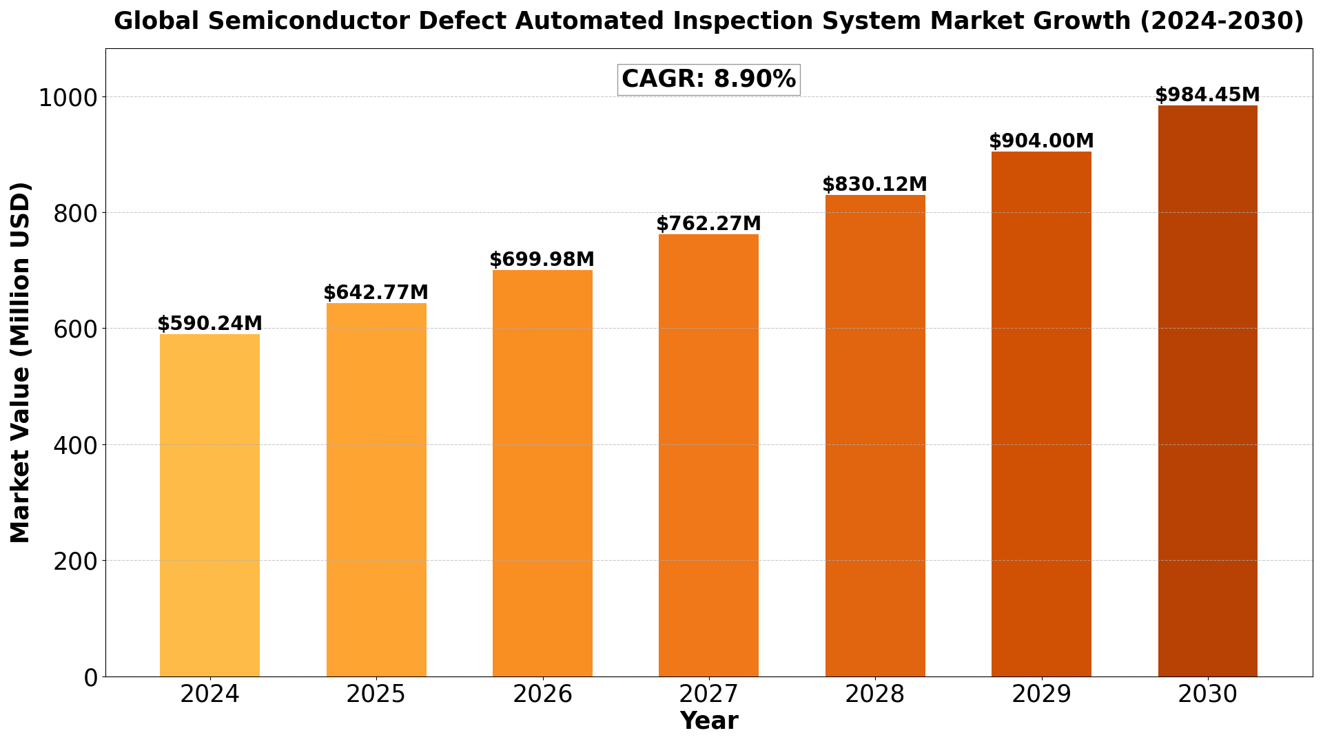
The Global Semiconductor Defect Automated Inspection System Market size was estimated at USD 542 million in 2023 and is projected to reach USD 984.45 million by 2030, exhibiting a CAGR of 8.90% during the forecast period.
North America Semiconductor Defect Automated Inspection System market size was USD 141.23 million in 2023, at a CAGR of 7.63% during the forecast period of 2024 through 2030.
Semiconductor Defect Automated Inspection System Key Market Trends :
- Increased Demand for Miniaturization: As semiconductors become more complex and miniaturized, the demand for advanced inspection systems that can detect defects at the nanoscale level is growing. Automated inspection systems are crucial for ensuring high-quality production in this highly competitive market.
- Advancement in AI and Machine Learning: Artificial intelligence (AI) and machine learning technologies are being integrated into semiconductor defect detection systems. These technologies enhance defect recognition, reduce human error, and improve the accuracy and speed of the inspection process.
- Rising Complexity of Semiconductor Designs: With the development of more advanced semiconductor devices for applications such as 5G, AI, and the Internet of Things (IoT), the complexity of the designs increases. Automated inspection systems are necessary to maintain quality and yield in these highly intricate designs.
- Increasing Adoption of Industry 4.0: The semiconductor industry is shifting toward Industry 4.0, characterized by the integration of digital technologies, automation, and data analytics. This trend promotes the use of automated inspection systems to optimize manufacturing processes and enhance product quality.
- Expanding Semiconductor Applications: As semiconductors are used in more industries, including automotive, healthcare, and consumer electronics, the need for defect-free products is rising. Automated inspection systems play a crucial role in ensuring the reliability and safety of semiconductor components used in these critical applications.
Semiconductor Defect Automated Inspection System Market Regional Analysis :

1. North America (USA, Canada, Mexico)
- USA: The largest market in the region due to advanced infrastructure, high disposable income, and technological advancements. Key industries include technology, healthcare, and manufacturing.
- Canada: Strong market potential driven by resource exports, a stable economy, and government initiatives supporting innovation.
- Mexico: A growing economy with strengths in automotive manufacturing, agriculture, and tourism, benefitting from trade agreements like the USMCA.
2. Europe (Germany, UK, France, Russia, Italy, Rest of Europe)
- Germany: The region’s industrial powerhouse with a focus on engineering, automotive, and machinery.
- UK: A hub for financial services, fintech, and pharmaceuticals, though Brexit has altered trade patterns.
- France: Strong in luxury goods, agriculture, and aerospace with significant innovation in renewable energy.
- Russia: Resource-driven economy with strengths in oil, gas, and minerals but geopolitical tensions affect growth.
- Italy: Known for fashion, design, and manufacturing, especially in luxury segments.
- Rest of Europe: Includes smaller yet significant economies like Spain, Netherlands, and Switzerland with strengths in finance, agriculture, and manufacturing.
3. Asia-Pacific (China, Japan, South Korea, India, Southeast Asia, Rest of Asia-Pacific)
- China: The largest market in the region with a focus on technology, manufacturing, and e-commerce. Rapid urbanization and middle-class growth fuel consumption.
- Japan: Technological innovation, particularly in robotics and electronics, drives the economy.
- South Korea: Known for technology, especially in semiconductors and consumer electronics.
- India: Rapidly growing economy with strengths in IT services, agriculture, and pharmaceuticals.
- Southeast Asia: Key markets like Indonesia, Thailand, and Vietnam show growth in manufacturing and tourism.
- Rest of Asia-Pacific: Emerging markets with growing investment in infrastructure and services.
4. South America (Brazil, Argentina, Colombia, Rest of South America)
- Brazil: Largest economy in the region, driven by agriculture, mining, and energy.
- Argentina: Known for agriculture exports and natural resources but faces economic instability.
- Colombia: Growing economy with strengths in oil, coffee, and flowers.
- Rest of South America: Includes Chile and Peru, which have strong mining sectors.
5. The Middle East and Africa (Saudi Arabia, UAE, Egypt, Nigeria, South Africa, Rest of MEA)
- Saudi Arabia: Oil-driven economy undergoing diversification with Vision 2030 initiatives.
- UAE: Financial hub with strengths in tourism, real estate, and trade.
- Egypt: Growing infrastructure development and tourism.
- Nigeria: Largest economy in Africa with strengths in oil and agriculture.
- South Africa: Industrialized economy with strengths in mining and finance.
- Rest of MEA: Includes smaller yet resource-rich markets like Qatar and Kenya with growing infrastructure investments.
Semiconductor Defect Automated Inspection System Market Segmentation :
The research report includes specific segments by region (country), manufacturers, Type, and Application. Market segmentation creates subsets of a market based on product type, end-user or application, Geographic, and other factors. By understanding the market segments, the decision-maker can leverage this targeting in the product, sales, and marketing strategies. Market segments can power your product development cycles by informing how you create product offerings for different segments.
Key Company
- KLA
- Hitachi
- Applied Materials
- Lasertec
- Advantest
- Onto Innovation
- Nikon
- Confovis
- Huagong Tech
- Yuweitk
- ENGITIST
- Optical Inspection
- Electron Beam Inspection (EBI)
- X-ray Inspection
- 4 and 5 Inches Wafer
- 6 Inches Wafer
- 8 Inches Wafer
- 12 Inches Wafer
Drivers
- Rising Demand for Semiconductor Devices: With the increasing applications of semiconductor devices across industries such as consumer electronics, automotive, telecommunications, and healthcare, there is a growing demand for high-performance semiconductors. Automated inspection systems are essential to ensure these devices meet stringent quality standards.
- Miniaturization and Complexity of Semiconductor Devices: As semiconductor devices continue to become smaller and more complex, the difficulty in detecting defects manually has increased. Automated inspection systems, which use advanced imaging, machine learning, and AI algorithms, have become indispensable in identifying even the tiniest defects, ensuring superior product quality.
- Technological Advancements in AI and Machine Learning: The integration of AI and machine learning in automated inspection systems enhances their accuracy, efficiency, and ability to learn from data. These systems can detect defects that might otherwise go unnoticed and improve over time by learning from new defect patterns.
- Increasing Need for Quality Control and Cost Reduction: As manufacturers aim to reduce production costs while maintaining high-quality standards, automated inspection systems are increasingly used to improve yield, reduce human error, and minimize wastage. This cost-saving ability is a major driver for the adoption of automated inspection systems in semiconductor manufacturing.
Restraints
- High Initial Investment: The capital required to invest in automated inspection systems is relatively high. This is a significant barrier, especially for smaller semiconductor manufacturers who might struggle to justify such an expense, even though the long-term benefits are considerable.
- Complexity of Integration into Existing Systems: Integrating automated inspection systems into existing semiconductor manufacturing lines can be technically challenging. It requires skilled personnel to manage the system and possible disruptions to current production schedules, which can delay ROI realization.
- Data Management Challenges: The vast amount of data generated by automated inspection systems can be overwhelming, and managing this data requires advanced storage solutions and robust data analysis capabilities. Without proper infrastructure, the potential of the inspection systems may not be fully realized.
Opportunities
- Expansion in Emerging Markets: As the semiconductor industry continues to grow globally, especially in emerging markets such as China, India, and Southeast Asia, there is significant potential for the adoption of automated inspection systems. These markets are rapidly scaling their semiconductor production capacity, creating new opportunities for the vendors in the market.
- Evolution of 5G and IoT: The advent of 5G technology and the rapid growth of the Internet of Things (IoT) are expected to drive demand for semiconductor devices, which in turn will boost the need for advanced automated inspection systems. The small size, low power consumption, and complex functionalities of semiconductors in 5G and IoT devices require precise defect detection.
- Advancements in Inspection Technologies: New technologies, such as advanced optical inspection, X-ray inspection, and electron beam inspection, offer new avenues for defect detection at unprecedented levels of precision. The continuous evolution of these technologies presents opportunities for further market growth and the development of more sophisticated inspection solutions.
- Customization and Software Integration: The demand for customized inspection solutions tailored to specific semiconductor types or production lines presents a major opportunity. Additionally, the integration of these systems with advanced software tools for predictive maintenance and analytics opens up new revenue streams for solution providers.
Challenges
- Lack of Skilled Labor: The increasing complexity of semiconductor manufacturing and automated inspection systems has created a gap in the availability of skilled labor capable of operating, maintaining, and optimizing these systems. This poses a challenge for manufacturers looking to implement automated solutions effectively.
- Competition from Low-Cost Solutions: The presence of low-cost, less advanced inspection systems from regional players in emerging markets creates price pressure. Manufacturers may opt for these less expensive systems, which can hinder the growth of high-end automated solutions in certain market segments.
- Technological Obsolescence: The rapid pace of technological advancement in semiconductor manufacturing can lead to the obsolescence of automated inspection systems. Companies must continuously innovate and upgrade their systems to remain competitive, adding to the complexity and cost of maintaining a state-of-the-art inspection system.
Key Benefits of This Market Research:
- Industry drivers, restraints, and opportunities covered in the study
- Neutral perspective on the market performance
- Recent industry trends and developments
- Competitive landscape & strategies of key players
- Potential & niche segments and regions exhibiting promising growth covered
- Historical, current, and projected market size, in terms of value
- In-depth analysis of the Semiconductor Defect Automated Inspection System Market
- Overview of the regional outlook of the Semiconductor Defect Automated Inspection System Market:
Key Reasons to Buy this Report:
- Access to date statistics compiled by our researchers. These provide you with historical and forecast data, which is analyzed to tell you why your market is set to change
- This enables you to anticipate market changes to remain ahead of your competitors
- You will be able to copy data from the Excel spreadsheet straight into your marketing plans, business presentations, or other strategic documents
- The concise analysis, clear graph, and table format will enable you to pinpoint the information you require quickly
- Provision of market value (USD Billion) data for each segment and sub-segment
- Indicates the region and segment that is expected to witness the fastest growth as well as to dominate the market
- Analysis by geography highlighting the consumption of the product/service in the region as well as indicating the factors that are affecting the market within each region
- Competitive landscape which incorporates the market ranking of the major players, along with new service/product launches, partnerships, business expansions, and acquisitions in the past five years of companies profiled
- Extensive company profiles comprising of company overview, company insights, product benchmarking, and SWOT analysis for the major market players
- The current as well as the future market outlook of the industry concerning recent developments which involve growth opportunities and drivers as well as challenges and restraints of both emerging as well as developed regions
- Includes in-depth analysis of the market from various perspectives through Porters five forces analysis
- Provides insight into the market through Value Chain
- Market dynamics scenario, along with growth opportunities of the market in the years to come
- 6-month post-sales analyst support
Customization of the Report
In case of any queries or customization requirements, please connect with our sales team, who will ensure that your requirements are met.
FAQs
Q1: What are Semiconductor Defect Automated Inspection Systems?
A1: Semiconductor Defect Automated Inspection Systems are advanced technologies used for detecting and analyzing defects in semiconductor manufacturing processes, ensuring high-quality production with minimal errors.
Q2: What is the current market size and forecast for the Semiconductor Defect Automated Inspection System market until 2032?
A2: The global market size was USD 542 million in 2023 and is projected to reach USD 984.45 million by 2030, with a CAGR of 8.90% during the forecast period.
Q3: What are the key growth drivers in the Semiconductor Defect Automated Inspection System market?
A3: Key growth drivers include increasing demand for high-performance semiconductors, advancements in semiconductor manufacturing technology, and the need for defect-free products to maintain product reliability.
Q4: Which regions dominate the Semiconductor Defect Automated Inspection System market?
A4: The Asia-Pacific region, particularly China, Japan, South Korea, and Taiwan, dominates the Semiconductor Defect Automated Inspection System market due to its large semiconductor manufacturing base.
Q5: What are the emerging trends in the Semiconductor Defect Automated Inspection System market?
A5: Emerging trends include the integration of AI and machine learning for defect detection, advancements in 3D inspection technologies, and the growing focus on miniaturization and high-precision manufacturing processes.

Get Sample Report PDF for Exclusive Insights
Report Sample Includes
- Table of Contents
- List of Tables & Figures
- Charts, Research Methodology, and more...