Semiconductor Defect Automated Inspection Equipment Market Overview
Semiconductor defect automated inspection equipment plays a crucial role in the semiconductor manufacturing process. It is used to detect and identify defects in semiconductor devices or chips, ensuring product quality and performance.
The analysis helps the reader to shape the competition within the industries and strategies for the competitive environment to enhance the potential profit. Furthermore, it provides a simple framework for evaluating and accessing the position of the business organization. The report structure also focuses on the competitive landscape of the Global Semiconductor Defect Automated Inspection Equipment Market, this report introduces in detail the market share, market performance, product situation, operation situation, etc. of the main players, which helps the readers in the industry to identify the main competitors and deeply understand the competition pattern of the market.
In a word, this report is a must-read for industry players, investors, researchers, consultants, business strategists, and all those who have any kind of stake or are planning to foray into the Semiconductor Defect Automated Inspection Equipment market in any manner.
Semiconductor Defect Automated Inspection Equipment Market Analysis:
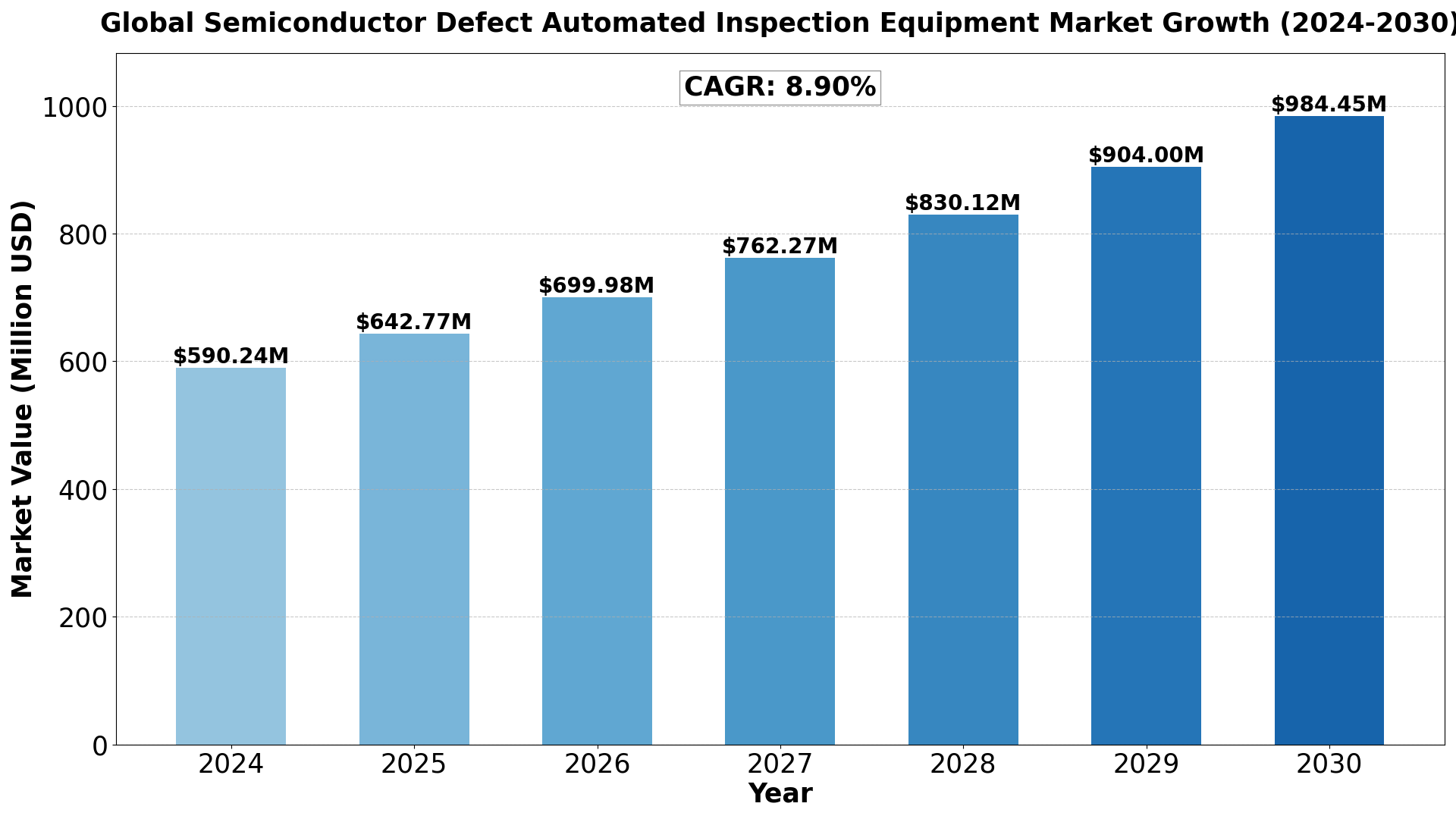
The Global Semiconductor Defect Automated Inspection Equipment Market size was estimated at USD 542 million in 2023 and is projected to reach USD 984.45 million by 2030, exhibiting a CAGR of 8.90% during the forecast period.
North America Semiconductor Defect Automated Inspection Equipment market size was USD 141.23 million in 2023, at a CAGR of 7.63% during the forecast period of 2024 through 2030.
Access Your Free Sample Report Now
Semiconductor Defect Automated Inspection Equipment Key Market Trends :
- Growing Demand for Advanced Inspection Technologies
The need for advanced automated inspection systems will increase as semiconductor manufacturing processes become more complex.
- Integration of AI and Machine Learning
AI-driven defect detection and machine learning algorithms will be increasingly integrated to enhance inspection accuracy and reduce false positives.
- Rise in Demand for Miniaturized Semiconductor Devices
As semiconductor devices shrink in size, the demand for precise and reliable inspection equipment will rise to meet the stricter quality control requirements.
- Increased Adoption of 3D Inspection Techniques
3D inspection technologies will gain traction to detect defects in complex semiconductor structures, improving overall inspection capabilities.
- Growth in End-Use Industries
With the growing applications of semiconductors in automotive, telecommunications, and consumer electronics, there will be a surge in demand for defect detection equipment to maintain product quality.
Semiconductor Defect Automated Inspection Equipment Market Regional Analysis :
1. North America (USA, Canada, Mexico)
- USA: The largest market in the region due to advanced infrastructure, high disposable income, and technological advancements. Key industries include technology, healthcare, and manufacturing.
- Canada: Strong market potential driven by resource exports, a stable economy, and government initiatives supporting innovation.
- Mexico: A growing economy with strengths in automotive manufacturing, agriculture, and tourism, benefitting from trade agreements like the USMCA.
2. Europe (Germany, UK, France, Russia, Italy, Rest of Europe)
- Germany: The region’s industrial powerhouse with a focus on engineering, automotive, and machinery.
- UK: A hub for financial services, fintech, and pharmaceuticals, though Brexit has altered trade patterns.
- France: Strong in luxury goods, agriculture, and aerospace with significant innovation in renewable energy.
- Russia: Resource-driven economy with strengths in oil, gas, and minerals but geopolitical tensions affect growth.
- Italy: Known for fashion, design, and manufacturing, especially in luxury segments.
- Rest of Europe: Includes smaller yet significant economies like Spain, Netherlands, and Switzerland with strengths in finance, agriculture, and manufacturing.
3. Asia-Pacific (China, Japan, South Korea, India, Southeast Asia, Rest of Asia-Pacific)
- China: The largest market in the region with a focus on technology, manufacturing, and e-commerce. Rapid urbanization and middle-class growth fuel consumption.
- Japan: Technological innovation, particularly in robotics and electronics, drives the economy.
- South Korea: Known for technology, especially in semiconductors and consumer electronics.
- India: Rapidly growing economy with strengths in IT services, agriculture, and pharmaceuticals.
- Southeast Asia: Key markets like Indonesia, Thailand, and Vietnam show growth in manufacturing and tourism.
- Rest of Asia-Pacific: Emerging markets with growing investment in infrastructure and services.
4. South America (Brazil, Argentina, Colombia, Rest of South America)
- Brazil: Largest economy in the region, driven by agriculture, mining, and energy.
- Argentina: Known for agriculture exports and natural resources but faces economic instability.
- Colombia: Growing economy with strengths in oil, coffee, and flowers.
- Rest of South America: Includes Chile and Peru, which have strong mining sectors.
5. The Middle East and Africa (Saudi Arabia, UAE, Egypt, Nigeria, South Africa, Rest of MEA)
- Saudi Arabia: Oil-driven economy undergoing diversification with Vision 2030 initiatives.
- UAE: Financial hub with strengths in tourism, real estate, and trade.
- Egypt: Growing infrastructure development and tourism.
- Nigeria: Largest economy in Africa with strengths in oil and agriculture.
- South Africa: Industrialized economy with strengths in mining and finance.
- Rest of MEA: Includes smaller yet resource-rich markets like Qatar and Kenya with growing infrastructure investments.
Semiconductor Defect Automated Inspection Equipment Market Segmentation :
The research report includes specific segments by region (country), manufacturers, Type, and Application. Market segmentation creates subsets of a market based on product type, end-user or application, Geographic, and other factors. By understanding the market segments, the decision-maker can leverage this targeting in the product, sales, and marketing strategies. Market segments can power your product development cycles by informing how you create product offerings for different segments.
Market Segmentation (by Type)
- Optical Inspection
- Electron Beam Inspection (EBI)
- X-ray Inspection
Market Segmentation (by Application)
- 4 and 5 Inches Wafer
- 6 Inches Wafer
- 8 Inches Wafer
- 12 Inches Wafer
Semiconductor Defect Automated Inspection Equipment Market Competitive landscape :
- KLA
- Hitachi
- Applied Materials
- Lasertec
- Advantest
- Onto Innovation
- Nikon
- Confovis
- Huagong Tech
- Yuweitk
- ENGITIST
Download Your Complimentary Sample Report
Drivers
- Rising Demand for Advanced Semiconductors: The growing adoption of smaller and more efficient semiconductor chips in electronics, AI, IoT, and 5G networks is fueling demand for automated inspection equipment. These tools are essential for ensuring high-quality manufacturing at the nanoscale level.
- Increased Use in Consumer Electronics: With the expansion of smartphones, wearables, and smart home devices, semiconductor manufacturing has grown exponentially, boosting the need for defect inspection equipment to maintain production yields.
- Stringent Quality Control Requirements: The push for zero-defect production, especially in critical industries like automotive and healthcare, drives investment in advanced inspection systems capable of detecting minute defects.
- Technological Advancements in AI and Machine Learning: Integration of AI and ML in inspection tools enhances defect detection accuracy and efficiency, leading to higher adoption rates in semiconductor fabs.
Restraints
- High Capital Investment: The initial cost of acquiring and implementing automated inspection equipment is significant, making it a challenge for smaller manufacturers to invest.
- Complexity of Implementation: Integrating these tools into existing production lines and adapting them to evolving semiconductor designs can be time-consuming and resource-intensive.
- Limited Skilled Workforce: The advanced nature of defect inspection technology requires a skilled workforce, which is currently in short supply, especially in emerging markets.
Opportunities
- Rising Demand for Advanced Driver Assistance Systems (ADAS): With the automotive sector’s growing reliance on semiconductors, particularly for ADAS and electric vehicles, inspection equipment tailored to automotive-grade chips offers significant opportunities.
- Emerging Semiconductor Markets: Countries like India, Vietnam, and Malaysia are ramping up semiconductor manufacturing, creating new demand for automated inspection systems.
- Focus on 3D and Advanced Packaging Technologies: As chip manufacturers move toward 3D packaging and advanced node designs, the need for highly precise defect inspection tools is growing rapidly.
Challenges
- Keeping Up with Rapid Technological Changes: The semiconductor industry evolves quickly, and inspection equipment must constantly adapt to new manufacturing processes, materials, and node sizes, which poses a significant challenge.
- Global Supply Chain Disruptions: Dependency on specific suppliers for high-tech components can delay equipment production and deployment, impacting the industry’s growth.
- Regulatory Barriers: Export controls and trade restrictions, especially for advanced semiconductor equipment, can limit market expansion in some regions.
Key Benefits of This Market Research:
- Industry drivers, restraints, and opportunities covered in the study
- Neutral perspective on the market performance
- Recent industry trends and developments
- Competitive landscape & strategies of key players
- Potential & niche segments and regions exhibiting promising growth covered
- Historical, current, and projected market size, in terms of value
- In-depth analysis of the Semiconductor Defect Automated Inspection Equipment Market
- Overview of the regional outlook of the Semiconductor Defect Automated Inspection Equipment Market:
Key Reasons to Buy this Report:
- Access to date statistics compiled by our researchers. These provide you with historical and forecast data, which is analyzed to tell you why your market is set to change
- This enables you to anticipate market changes to remain ahead of your competitors
- You will be able to copy data from the Excel spreadsheet straight into your marketing plans, business presentations, or other strategic documents
- The concise analysis, clear graph, and table format will enable you to pinpoint the information you require quickly
- Provision of market value (USD Billion) data for each segment and sub-segment
- Indicates the region and segment that is expected to witness the fastest growth as well as to dominate the market
- Analysis by geography highlighting the consumption of the product/service in the region as well as indicating the factors that are affecting the market within each region
- Competitive landscape which incorporates the market ranking of the major players, along with new service/product launches, partnerships, business expansions, and acquisitions in the past five years of companies profiled
- Extensive company profiles comprising of company overview, company insights, product benchmarking, and SWOT analysis for the major market players
- The current as well as the future market outlook of the industry concerning recent developments which involve growth opportunities and drivers as well as challenges and restraints of both emerging as well as developed regions
- Includes in-depth analysis of the market from various perspectives through Porters five forces analysis
- Provides insight into the market through Value Chain
- Market dynamics scenario, along with growth opportunities of the market in the years to come
- 6-month post-sales analyst support
Customization of the Report
In case of any queries or customization requirements, please connect with our sales team, who will ensure that your requirements are met.

Get Sample Report PDF for Exclusive Insights
Report Sample Includes
- Table of Contents
- List of Tables & Figures
- Charts, Research Methodology, and more...