➣ Global Plasma Surface Treatment Equipment for Semiconductor Market Overview
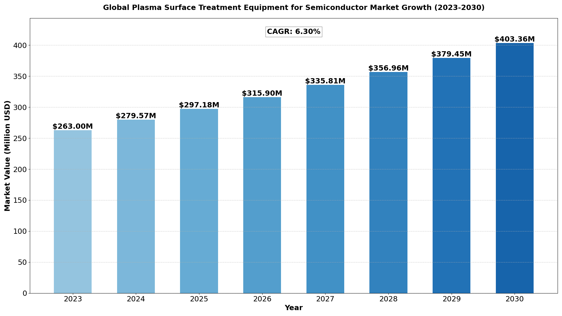
The global Plasma Surface Treatment Equipment for Semiconductor market size was estimated at USD 263 million in 2023 and is projected to reach USD 403.36 million by 2030, exhibiting a CAGR of 6.30% during the forecast period.
North America Plasma Surface Treatment Equipment for Semiconductor market size was USD 68.53 million in 2023, at a CAGR of 5.40% during the forecast period of 2024 through 2030.
Plasma surface treatment equipment can be used in the semiconductor industry in processes such as precision cleaning, surface activation, stripper and etching, and flip chip packaging.
This report provides a deep insight into the global Plasma Surface Treatment Equipment for Semiconductor market covering all its essential aspects. This ranges from a macro overview of the market to micro details of the market size, competitive landscape, development trend, niche market, key market drivers and challenges, SWOT analysis, value chain analysis, etc.
The analysis helps the reader to shape the competition within the industries and strategies for the competitive environment to enhance the potential profit. Furthermore, it provides a simple framework for evaluating and accessing the position of the business organization. The report structure also focuses on the competitive landscape of the Global Plasma Surface Treatment Equipment for Semiconductor Market, this report introduces in detail the market share, market performance, product situation, operation situation, etc. of the main players, which helps the readers in the industry to identify the main competitors and deeply understand the competition pattern of the market.
In a word, this report is a must-read for industry players, investors, researchers, consultants, business strategists, and all those who have any kind of stake or are planning to foray into the Plasma Surface Treatment Equipment for Semiconductor market in any manner.
Global Plasma Surface Treatment Equipment for Semiconductor Market: Market Segmentation Analysis
The research report includes specific segments by region (country), manufacturers, Type, and Application. Market segmentation creates subsets of a market based on product type, end-user or application, Geographic, and other factors. By understanding the market segments, the decision-maker can leverage this targeting in the product, sales, and marketing strategies. Market segments can power your product development cycles by informing how you create product offerings for different segments.
Click Here to Download Your Free Sample Report
Key Company
- Nordson
- PVA TePla
- Panasonic
- Shenzhen OKSUN Technology
- Tonson Tech
- Vision Semicon
- Yield Engineering Systems
- CRF Plasma
- Tantec
- FARI
- Samco
- PINK GmbH Thermosysteme
Market Segmentation (by Type)
- Low Pressure/Vacuum Plasma Surface Treatment Equipment
- Atmospheric Plasma Surface Treatment Equipment
Market Segmentation (by Application)
- Chip Bonding
- Lead Frame
- Others
Geographic Segmentation
- North America (USA, Canada, Mexico)
- Europe (Germany, UK, France, Russia, Italy, Rest of Europe)
- Asia-Pacific (China, Japan, South Korea, India, Southeast Asia, Rest of Asia-Pacific)
- South America (Brazil, Argentina, Columbia, Rest of South America)
- The Middle East and Africa (Saudi Arabia, UAE, Egypt, Nigeria, South Africa, Rest of MEA)
➣ Key Benefits of This Market Research:
- Industry drivers, restraints, and opportunities covered in the study
- Neutral perspective on the market performance
- Recent industry trends and developments
- Competitive landscape & strategies of key players
- Potential & niche segments and regions exhibiting promising growth covered
- Historical, current, and projected market size, in terms of value
- In-depth analysis of the Plasma Surface Treatment Equipment for Semiconductor Market
- Overview of the regional outlook of the Plasma Surface Treatment Equipment for Semiconductor Market:
➣ Key Reasons to Buy this Report:
- Access to date statistics compiled by our researchers. These provide you with historical and forecast data, which is analyzed to tell you why your market is set to change
- This enables you to anticipate market changes to remain ahead of your competitors
- You will be able to copy data from the Excel spreadsheet straight into your marketing plans, business presentations, or other strategic documents
- The concise analysis, clear graph, and table format will enable you to pinpoint the information you require quickly
- Provision of market value (USD Billion) data for each segment and sub-segment
- Indicates the region and segment that is expected to witness the fastest growth as well as to dominate the market
- Analysis by geography highlighting the consumption of the product/service in the region as well as indicating the factors that are affecting the market within each region
- Competitive landscape which incorporates the market ranking of the major players, along with new service/product launches, partnerships, business expansions, and acquisitions in the past five years of companies profiled
- Extensive company profiles comprising of company overview, company insights, product benchmarking, and SWOT analysis for the major market players
- The current as well as the future market outlook of the industry concerning recent developments which involve growth opportunities and drivers as well as challenges and restraints of both emerging as well as developed regions
- Includes in-depth analysis of the market from various perspectives through Porters five forces analysis
- Provides insight into the market through Value Chain
- Market dynamics scenario, along with growth opportunities of the market in the years to come
- 6-month post-sales analyst support
Click Here to Download Your Free Sample Report
Customization of the Report
In case of any queries or customization requirements, please connect with our sales team, who will ensure that your requirements are met.
➣ Drivers
- Growing Demand for Advanced Semiconductor Devices: The increasing complexity and miniaturization of semiconductor devices require precise surface treatment processes. Plasma surface treatment equipment offers enhanced cleaning, etching, and deposition, which are crucial for advanced semiconductor manufacturing.
- Technological Advancements: Continuous innovations in plasma surface treatment technology, such as the development of low-temperature plasma and atmospheric pressure plasma systems, enhance process efficiency and expand application areas.
- Expansion of the Semiconductor Industry: The global semiconductor industry’s growth, driven by the rising adoption of electronics in various sectors like automotive, consumer electronics, and industrial automation, boosts the demand for plasma surface treatment equipment.
- Rising Adoption of IoT and 5G: The proliferation of IoT devices and the rollout of 5G networks demand higher performance and reliability from semiconductor components, necessitating advanced surface treatment solutions to ensure optimal performance and longevity.
- Environmental Regulations: Stricter environmental regulations on the use of hazardous chemicals in semiconductor manufacturing are prompting the industry to adopt plasma surface treatment, which is a cleaner and more sustainable alternative.
➣ Restraints
- High Initial Investment: The substantial capital required to acquire and install plasma surface treatment equipment poses a significant barrier, especially for small and medium-sized enterprises (SMEs).
- Complex Maintenance Requirements: Plasma equipment requires regular maintenance and skilled personnel to operate, which can increase operational costs and complicate adoption for some manufacturers.
- Competition from Alternative Technologies: Other surface treatment technologies, such as chemical etching and mechanical cleaning, still hold a significant share of the market, providing competition to plasma-based methods.
➣ Opportunities
- Expansion into Emerging Markets: Rapid industrialization and the growth of the semiconductor industry in emerging economies present lucrative opportunities for plasma surface treatment equipment manufacturers.
- Integration with Automation and AI: The integration of plasma treatment systems with automation and AI can improve process control and efficiency, opening up new possibilities for innovation in semiconductor manufacturing.
- R&D in New Applications: Continuous research and development to find new applications for plasma technology in semiconductor manufacturing, such as advanced packaging and flexible electronics, can drive market growth.
- Collaborations and Partnerships: Collaborations between equipment manufacturers and semiconductor companies for developing customized plasma solutions can lead to tailored equipment that meets specific industry needs.
➣ Challenges
- Technological Complexity: The complexity of plasma surface treatment processes and the need for precise control over various parameters make it challenging for manufacturers to achieve consistent results, especially in high-volume production.
- Market Volatility: The semiconductor industry is subject to cyclical demand and supply fluctuations, which can impact the investment in and adoption of new equipment like plasma surface treatment systems.
- Skilled Workforce Shortage: A shortage of skilled technicians and engineers who can operate and maintain sophisticated plasma equipment may hinder the market’s growth.
- Regulatory Hurdles: Navigating the various safety and environmental regulations associated with plasma technology can be challenging, particularly in regions with stringent regulatory frameworks.
Interested in related market reports? Click here to explore more!
➣ About Semiconductor Insight:
Established in 2016, Semiconductor Insight specializes in providing comprehensive semiconductor industry research and analysis to support businesses in making well-informed decisions within this dynamic and fast-paced sector. From the beginning, we have been committed to delivering in-depth semiconductor market research, identifying key trends, opportunities, and challenges shaping the global semiconductor industry.
Our expertly developed semiconductor market reports offer actionable intelligence, including detailed semiconductor industry analysis, market forecasts, competitive analysis, and insights into technological advancements, enabling our clients to maintain a competitive edge. With nearly a decade of expertise, we remain at the forefront of innovation, delivering strategic clarity to businesses in the semiconductor sector.
Our commitment to providing insights into semiconductor market share and industry trends ensures that our clients have the information they need to succeed in the ever-evolving semiconductor market.
Get Sample Report PDF for Exclusive Insights
Report Sample Includes
- Table of Contents
- List of Tables & Figures
- Charts, Research Methodology, and more...