Patterning Materials Market Overview
Patterning is the backbone of scaling, which has reduced the size of the transistor to where it is today, in turn making modern electronic devices increasingly affordable. This report analzyed the materials for patterning.
This report provides a deep insight into the global Patterning Materials market covering all its essential aspects. This ranges from a macro overview of the market to micro details of the market size, competitive landscape, development trend, niche market, key market drivers and challenges, SWOT analysis, value chain analysis, etc.
The analysis helps the reader to shape the competition within the industries and strategies for the competitive environment to enhance the potential profit. Furthermore, it provides a simple framework for evaluating and accessing the position of the business organization. The report structure also focuses on the competitive landscape of the Global Patterning Materials Market, this report introduces in detail the market share, market performance, product situation, operation situation, etc. of the main players, which helps the readers in the industry to identify the main competitors and deeply understand the competition pattern of the market.
In a word, this report is a must-read for industry players, investors, researchers, consultants, business strategists, and all those who have any kind of stake or are planning to foray into the Patterning Materials market in any manner.
Patterning Materials Market Analysis:
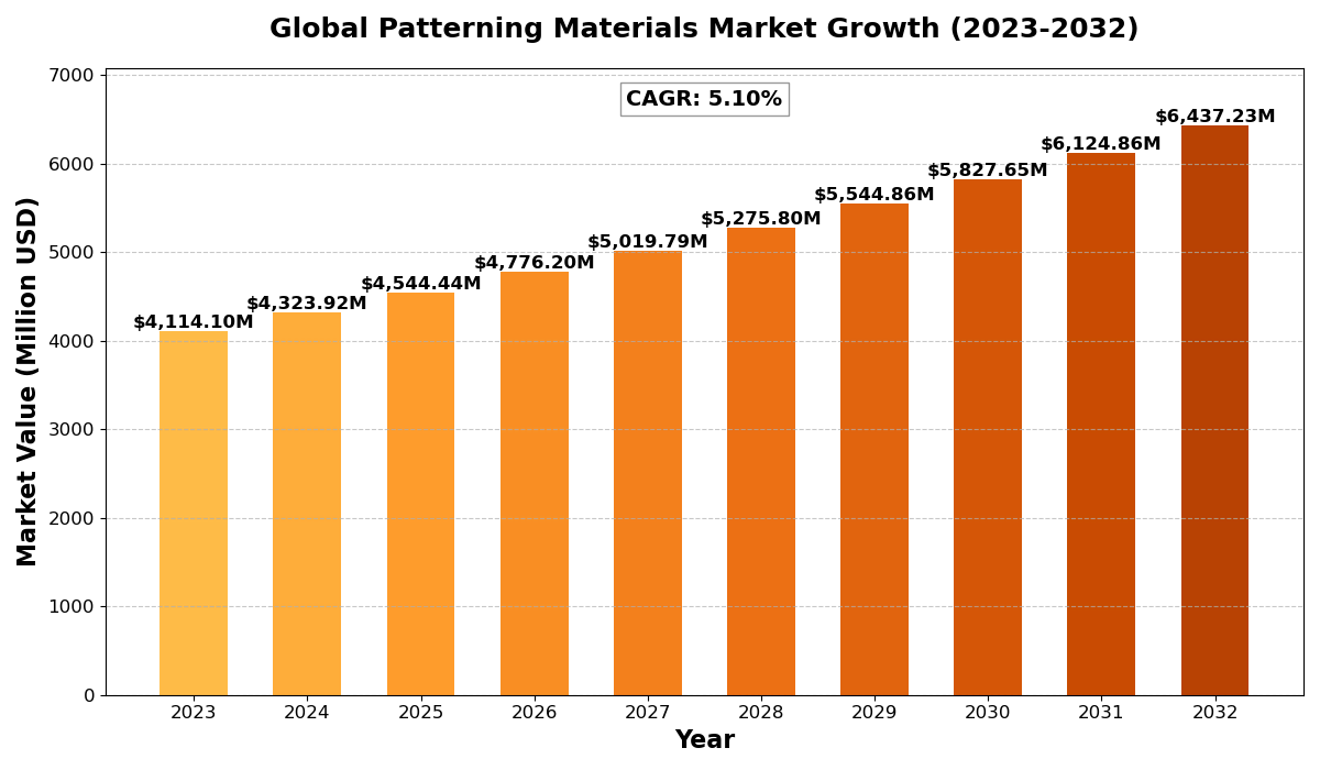
The Global Patterning Materials Market size was estimated at USD 4114.10 million in 2023 and is projected to reach USD 6437.23 million by 2032, exhibiting a CAGR of 5.10% during the forecast period.
North America Patterning Materials market size was estimated at USD 1167.79 million in 2023, at a CAGR of 4.37% during the forecast period of 2025 through 2032.
Patterning Materials Key Market Trends :
-
Miniaturization of Electronic Devices
The continual trend of reducing the size of electronic devices, such as transistors, has been a significant factor driving the patterning materials market. This trend leads to a growing demand for more advanced materials capable of handling smaller, intricate patterns. -
Increased Focus on Semiconductor Manufacturing
As semiconductor technologies advance, patterning materials play a crucial role in creating precise patterns for the production of integrated circuits. This focus on semiconductor growth fuels demand in various applications, from automotive to consumer electronics. -
Rise in Demand for MEMS and NEMS Devices
Microelectromechanical systems (MEMS) and nanoelectromechanical systems (NEMS) require high-performance patterning materials. As industries such as automotive and healthcare adopt these technologies, the demand for suitable materials is expected to increase. -
Integration of Advanced Lithography Techniques
The integration of advanced lithography techniques, like extreme ultraviolet (EUV) lithography, is revolutionizing the patterning materials industry. These techniques help achieve finer patterns, which are required for the next-generation microchips and devices. -
Sustainability and Eco-friendly Alternatives
With growing concerns over environmental impact, there is a significant trend toward developing eco-friendly patterning materials. The industry is moving toward materials that are not only efficient but also sustainable in the long run.
Patterning Materials Market Regional Analysis :
-
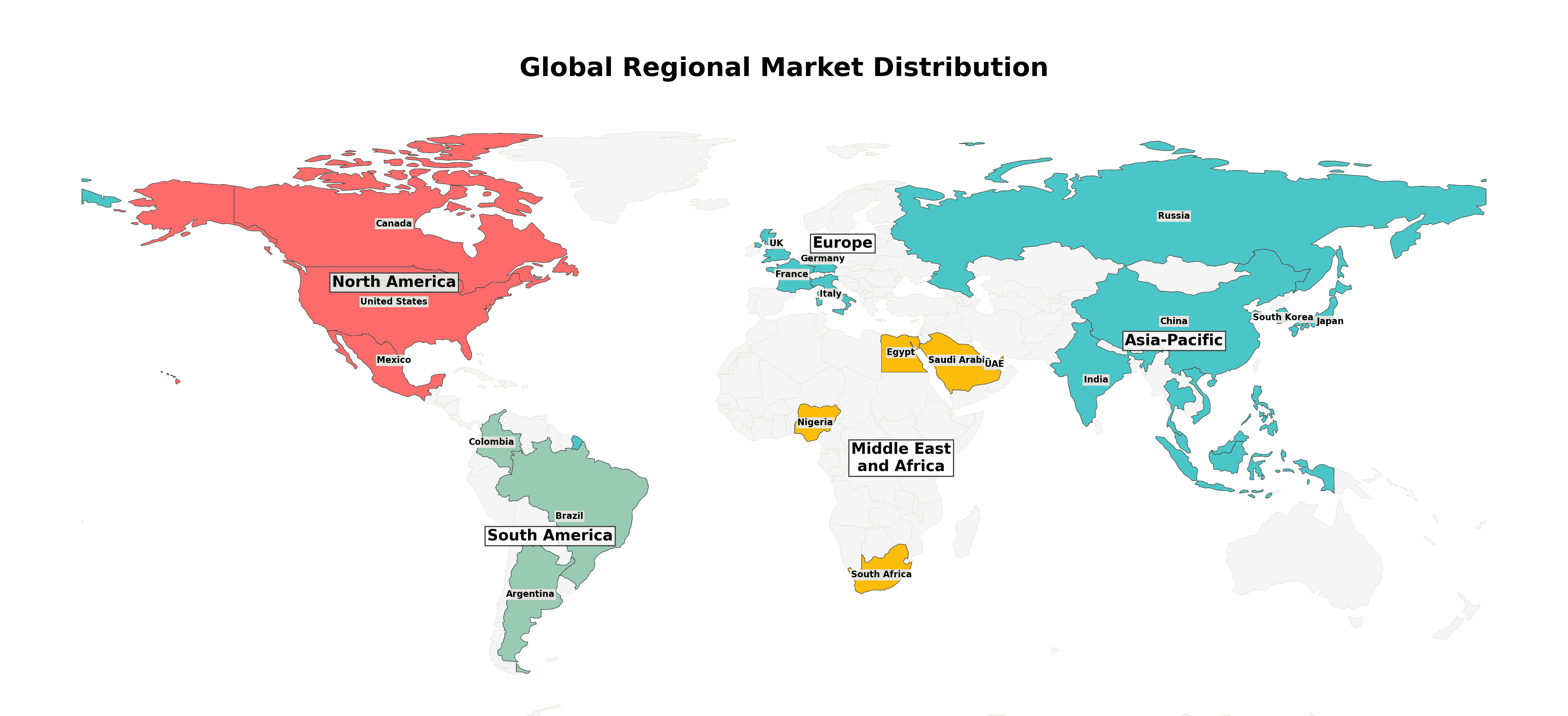
North America:
Strong demand driven by EVs, 5G infrastructure, and renewable energy, with the U.S. leading the market.
-
Europe:
Growth fueled by automotive electrification, renewable energy, and strong regulatory support, with Germany as a key player.
-
Asia-Pacific:
Dominates the market due to large-scale manufacturing in China and Japan, with growing demand from EVs, 5G, and semiconductors.
-
South America:
Emerging market, driven by renewable energy and EV adoption, with Brazil leading growth.
-
Middle East & Africa:
Gradual growth, mainly due to investments in renewable energy and EV infrastructure, with Saudi Arabia and UAE as key contributors.
Patterning Materials Market Segmentation :
The research report includes specific segments by region (country), manufacturers, Type, and Application. Market segmentation creates subsets of a market based on product type, end-user or application, Geographic, and other factors. By understanding the market segments, the decision-maker can leverage this targeting in the product, sales, and marketing strategies. Market segments can power your product development cycles by informing how you create product offerings for different segments.
Key Company
- Fujifilm Holdings Corporation
- JSR Micro
- Inc.
- Dongjin Semichem Co.
- Ltd.
- Honeywell Electronic Materials
- Inc.
- Shin-Etsu Chemical Co.
- Ltd.
- DowDuPont
- Tokyo Ohka Kogyo Co.
- Ltd. (Tok)
- Sumitomo Chemicals Co.
- Ltd.
- Microchem Corporation
- Brewer Science
- Inc.
Market Segmentation (by Type)
- 193 NM Immersion Resist
- Positive 193 NM Dry Resist
- Positive 248 NM Resist
- I-Line and G-Line Resist
- Others
Market Segmentation (by Application)
- Automotive Sensors
- DRAM
- Glass Printed Circuit Boards
- MEMS & NEMS Devices
- Others
Market Drivers
-
Technological Advancements in Electronics Manufacturing
Continuous improvements in electronic devices, driven by miniaturization and the increasing need for powerful chips, directly contribute to the rising demand for innovative patterning materials. -
Growing Semiconductor Industry
The expanding semiconductor industry, which plays a pivotal role in multiple sectors like automotive, consumer electronics, and communication, drives the need for advanced patterning solutions. -
Rising Applications in MEMS/NEMS and Automotive Sensors
The increased use of MEMS and NEMS in various industries, particularly for automotive sensors and other smart technologies, accelerates demand for high-quality patterning materials.
Market Restraints
-
High Cost of Advanced Patterning Materials
The development and production of advanced patterning materials, such as 193 nm immersion resist and positive 248 nm resist, can be expensive, limiting accessibility for some industries and companies. -
Complex Manufacturing Processes
The intricate and complex manufacturing processes required for high-precision patterning materials can result in delays, increased production costs, and technical challenges. -
Availability of Alternative Technologies
The growth of alternative technologies, like nanoimprint lithography, might pose a challenge to the widespread adoption of conventional patterning materials.
Market Opportunities
-
Expansion of 5G and IoT Technologies
The growing demand for 5G networks and IoT devices presents an opportunity for the patterning materials market, as these technologies require high-performance semiconductors and miniaturized components. -
Development of Eco-friendly Patterning Materials
As the demand for sustainable solutions rises, there are significant opportunities for developing and adopting eco-friendly patterning materials that meet the needs of modern electronics while reducing environmental impact. -
Technological Collaboration and Strategic Partnerships
Partnerships between key players and advancements in R&D can offer new opportunities for the development of cutting-edge patterning materials, enabling companies to stay competitive in the evolving market.
Market Challenges
-
Rapid Technological Changes
The rapid pace of technological evolution in the semiconductor and electronics industries poses challenges for patterning material suppliers to keep up with the latest innovations. -
Regulatory and Environmental Constraints
As regulations regarding the environmental impact of manufacturing processes become stricter, the industry faces challenges in meeting both regulatory requirements and market demands. -
Supply Chain Disruptions
The complexity of the global supply chain for patterning materials can lead to disruptions, such as delays in production or scarcity of raw materials, which could affect overall market growth.
Key Benefits of This Market Research:
- Industry drivers, restraints, and opportunities covered in the study
- Neutral perspective on the market performance
- Recent industry trends and developments
- Competitive landscape & strategies of key players
- Potential & niche segments and regions exhibiting promising growth covered
- Historical, current, and projected market size, in terms of value
- In-depth analysis of the Patterning Materials Market
- Overview of the regional outlook of the Patterning Materials Market:
Key Reasons to Buy this Report:
- Access to date statistics compiled by our researchers. These provide you with historical and forecast data, which is analyzed to tell you why your market is set to change
- This enables you to anticipate market changes to remain ahead of your competitors
- You will be able to copy data from the Excel spreadsheet straight into your marketing plans, business presentations, or other strategic documents
- The concise analysis, clear graph, and table format will enable you to pinpoint the information you require quickly
- Provision of market value data for each segment and sub-segment
- Indicates the region and segment that is expected to witness the fastest growth as well as to dominate the market
- Provides insight into the market through Value Chain
- Market dynamics scenario, along with growth opportunities of the market in the years to come
- 6-month post-sales analyst support
Customization of the Report
In case of any queries or customization requirements, please connect with our sales team, who will ensure that your requirements are met.
FAQs
Q1: What are the key driving factors and opportunities in the Patterning Materials market?
A1: The key drivers include technological advancements in electronics, the growth of the semiconductor industry, and the increasing demand for MEMS/NEMS devices. Opportunities lie in the rise of 5G and IoT technologies, the development of eco-friendly materials, and strategic collaborations in R&D.
Q2: Which region is projected to have the largest market share?
A2: North America is expected to have the largest market share, with the market size estimated at USD 1167.79 million in 2023 and a CAGR of 4.37% during the forecast period of 2025-2032.
Q3: Who are the top players in the global Patterning Materials market?
A3: The leading players include Fujifilm Holdings Corporation, JSR Micro Inc., Dongjin Semichem Co. Ltd., Honeywell Electronic Materials Inc., and Shin-Etsu Chemical Co. Ltd.
Q4: What are the latest technological advancements in the industry?
A4: Recent advancements include the integration of extreme ultraviolet (EUV) lithography, innovations in immersion resist technologies, and the development of eco-friendly patterning materials.
Q5: What is the current size of the global Patterning Materials market?
A5: The global Patterning Materials market was valued at USD 4114.10 million in 2023 and is projected to reach USD 6437.23 million by 2032, growing at a CAGR of 5.10% during the forecast period.

Get Sample Report PDF for Exclusive Insights
Report Sample Includes
- Table of Contents
- List of Tables & Figures
- Charts, Research Methodology, and more...
 Download Sample Report PDF