Glass Substrate TGV Market Insights
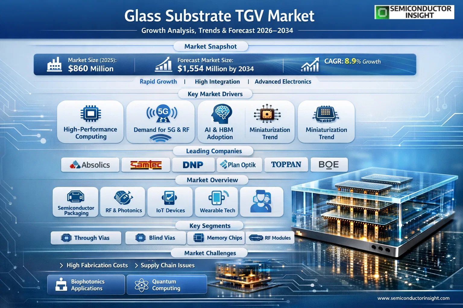
Global Glass Substrate TGV market size was valued at USD 860 million in 2025. The market is projected to grow from USD 935 million in 2026 to USD 1,554 million by 2034, exhibiting a CAGR of 8.9% during the forecast period.
Glass Substrate TGV stands for Through-Glass Vias, a critical technology in advanced semiconductor packaging. These are microscopic vertical interconnects formed by creating and metallizing holes through a glass substrate, enabling high-density electrical connections between stacked chips or components. This technology is crucial for applications demanding superior signal integrity, thermal management, and miniaturization, such as high-bandwidth memory (HBM), radio-frequency (RF) modules, and advanced sensors.
The market is experiencing robust growth driven by the relentless demand for higher performance and greater integration in electronics, particularly for artificial intelligence (AI) accelerators and 5G/6G communication systems. Furthermore, the push towards heterogeneous integration and 3D packaging solutions is creating significant demand for TGV-based interposers as a superior alternative to silicon. Key industry players are actively expanding capacity; for instance, Absolics (an SKC subsidiary) announced a major investment in 2023 to build a glass substrate production facility in Georgia, USA, targeting the AI chip market. Other leading companies operating with diverse portfolios include Plan Optik AG, Samtec Microelectronics, Toppan Printing Co., Ltd., and BOE Technology Group.
MARKET DRIVERS
Advancements in High-Performance Computing and Packaging
The relentless push for miniaturization and higher bandwidth in semiconductor devices is a primary driver for Glass Substrate TGV market. Glass substrates, with their superior electrical properties and dimensional stability compared to organic alternatives, are becoming critical for advanced integrated circuit packaging. The increasing demand for 2.5D and 3D heterogeneous integration in applications like artificial intelligence accelerators and high-bandwidth memory (HBM) is accelerating market adoption. This shift is largely driven by major semiconductor manufacturers investing in glass core technology for next-generation products.
Growing Demand for Advanced RF and Photonic Components
The proliferation of 5G, 6G, and automotive radar systems necessitates components with exceptional signal integrity at high frequencies. Glass Substrate TGV technology offers ultra-low transmission loss and excellent insulation, making it ideal for radio frequency (RF) filters, antennas, and photonic interposers. This positions Glass Substrate TGV market as an enabler for telecommunications infrastructure and automotive electronics, where performance and reliability are paramount.
➤ Market analysts project the increasing complexity of semiconductor packages and the superior material properties of glass will sustain double-digit growth for the TGV sector over the next five years.
Furthermore, the expansion of the Internet of Things (IoT) and wearable devices creates demand for compact, high-performance sensors and modules, which are well-suited to the thin profiles and fine-pitch via capabilities of glass substrates.
MARKET CHALLENGES
High Fabrication Costs and Supply Chain Complexities
Despite its advantages, Glass Substrate TGV market faces significant challenges. The cost of specialized glass materials and the capital-intensive nature of via formation processes, such as laser or plasma etching, remain high. Establishing a robust, high-volume supply chain for large-format, defect-free glass panels suitable for semiconductor manufacturing is complex and requires significant investment, potentially slowing widespread adoption in cost-sensitive applications.
Other Challenges
Technical and Integration Hurdles
Precision handling of thin glass substrates without breakage during panel-level processing requires advanced manufacturing techniques. Furthermore, achieving reliable hermetic sealing and managing the coefficient of thermal expansion (CTE) mismatch between glass and other semiconductor materials presents ongoing engineering challenges that must be overcome.
Competition from Established Materials
Silicon and organic substrates have a mature, cost-optimized manufacturing ecosystem. Convincing manufacturers to transition to a newer material like glass for through-glass vias requires demonstrated, unambiguous performance benefits and reliable volume production, creating a significant barrier to rapid market penetration.
MARKET RESTRAINTS
Limited Standardization and High Initial Investment
A key restraint on Glass Substrate TGV market is the current lack of industry-wide standardization for materials, via dimensions, and testing protocols. This uncertainty can deter investment and complicate design implementation for OEMs. Additionally, the initial capital expenditure required to establish or retool production lines for TGV technology is substantial, which may limit entry to only the largest semiconductor foundries and packaging houses, thereby constraining the overall market growth rate in the near term.
MARKET OPPORTUNITIES
Expansion into Biophotonics and Quantum Computing
The unique properties of glass substrates present significant growth opportunities beyond traditional electronics. In biophotonics and medical diagnostics, glass is biocompatible and transparent, allowing for the integration of fluidic channels and optical waveguides with electrical interconnects via TGVs for advanced lab-on-a-chip devices. This convergence opens new application verticals for Glass Substrate TGV market.
Collaborative Ecosystem Development
There is a major opportunity for collaborative development between glass manufacturers, equipment suppliers, and semiconductor companies to drive down costs and improve yields. Strategic partnerships aimed at standardizing processes and developing turnkey manufacturing solutions can accelerate market maturation. Furthermore, the push for energy-efficient computing and novel architectures for data centers and quantum computing could leverage the low-loss characteristics of glass interposers, creating a substantial long-term opportunity for Glass Substrate TGV market.
Glass Substrate TGV Market Trends
Focus on Enhanced Performance and Integration
Glass Substrate TGV market is primarily driven by the demand for higher performance and greater component integration in advanced electronics. Specifically, the rise of artificial intelligence accelerators and high-bandwidth memory (HBM) requires packaging solutions that offer superior electrical performance, which TGVs provide through their excellent insulating properties and fine-pitch capability. This trend is making TGV technology a critical enabler for next-generation data center hardware and communication systems where speed and signal integrity are paramount.
Other Trends
Advancements in Fabrication Technology
The market trend shows continuous innovation in fabrication processes to achieve smaller via diameters and higher aspect ratios. This push for miniaturization allows for greater interconnect density within the Glass Substrate TGV, which is essential for creating more powerful and compact chips. Leading manufacturers are investing in advanced laser drilling and metallization techniques to improve yields and manufacturability at these demanding specifications.
Material and Application Diversification
Beyond traditional microelectronics, Glass Substrate TGV technology is being explored for new applications in markets like microfluidics and photonics. Concurrently, research into specialized glass compositions aims to improve thermal and mechanical properties for more robust packages. This diversification effort seeks to broaden the commercial appeal and address specific challenges in high-frequency and high-power environments.
Industry Emphasis on Cost Optimization
As Glass Substrate TGV market moves towards higher-volume adoption, significant focus is placed on optimizing manufacturing costs. This involves refining process flows to increase throughput and yield, which is critical for expanding the technology’s use beyond flagship products into a wider range of semiconductor packaging applications. The overall trend is toward establishing TGV as a commercially scalable and competitive solution in the advanced packaging landscape.
COMPETITIVE LANDSCAPE
Key Industry Players
A high-growth market driven by advanced electronics integration and heterogeneous packaging demand.
Glass Substrate TGV market is characterized by a dynamic and evolving competitive structure, where technology leadership and manufacturing scale are critical. Currently, the market is led by specialized materials and advanced packaging manufacturers who have successfully commercialized TGV fabrication processes. Absolics, a subsidiary of SK Inc. dedicated to glass material solutions, is identified as a significant leader, capitalizing on its pioneering development of large-area, high-quality glass substrates designed for TGV applications. Other established Japanese and Korean players, including DNP (Dai Nippon Printing) and Samtec, hold considerable market share due to their deep expertise in fine-precision patterning, etching, and metallization processes essential for high-density interconnects. The competitive intensity is increasing as the technology transitions from R&D to high-volume manufacturing for applications like High-Bandwidth Memory (HBM) and AI accelerators, where performance and yield are paramount.
Beyond these primary players, a vibrant ecosystem of niche innovators and specialized foundries is emerging. Companies such as Plan Optik, Tecnisco, and Toppan leverage their expertise in specialty glass and microfabrication to serve diverse market segments. In parallel, regional players in the Asia-Pacific market, particularly in China, are rapidly advancing. Firms like BOE, Sky Semiconductor, and Hefei Zhongke Daojing are making strategic investments to build domestic capacity and secure supply chains for semiconductor packaging. This multi-tiered landscape also includes technology-focused entities such as Kiso Wave (specializing in high-frequency components) and Glassmicro, which are driving innovation in via formation techniques and new glass compositions. The market’s trajectory suggests ongoing consolidation and partnership formation as manufacturing challenges require combined expertise in materials science, laser processing, and advanced semiconductor packaging.
List of Key Glass Substrate TGV Companies Profiled
- Absolics (SK)
- Samtec
- DNP (Dai Nippon Printing)
- NSC (Nippon Electric Glass)
- Plan Optik AG
- Nanosystems JP
- Tecnisco Ltd.
- Kiso Wave Co., Ltd.
- Toppan Inc.
- MICRO
- WG TECH
- BOE Technology Group
- Sky Semiconductor
- AKM Meadville
- Hefei Zhongke Daojing
Segment Analysis:
| Segment Category | Sub-Segments | Key Insights |
| By Type |
|
Through Vias represent the leading segment, driven by their superior performance in creating vertical interconnects for complex, multi-layered packaging architectures. This dominance is anchored in their critical role in enabling true 3D integration, which is fundamental for next-generation electronics. The technology facilitates a direct electrical pathway through the entire glass substrate, which is essential for stacking memory and processing dies in high-bandwidth applications. Furthermore, the fabrication process for through vias, though challenging, is increasingly matured by key industry players, making it the preferred solution for applications demanding the highest interconnect density and signal integrity. |
| By Application |
|
Memory Chip packaging is the predominant application segment, fueled by the explosive demand for High-Bandwidth Memory (HBM) in artificial intelligence and data centers. TGV technology is uniquely positioned to address the stringent requirements of memory packaging, such as minimizing signal delay and crosstalk while achieving extreme miniaturization. The inherent electrical properties of glass substrates, including low dielectric loss and excellent high-frequency performance, make TGVs ideal for the dense, high-speed interconnects required in modern memory stacks. This segment’s growth is directly tied to the semiconductor industry’s relentless pursuit of higher performance per watt in computing. |
| By End User |
|
Semiconductor Foundries & IDMs lead as the primary end-users, integrating TGV technology directly into their cutting-edge product roadmaps for high-performance computing and communication chips. Their leadership stems from the strategic necessity to control advanced packaging technologies, which are now a key differentiator for chip performance. These companies drive innovation by investing in proprietary TGV fabrication processes and collaborating with material suppliers to push the limits of via density and aspect ratio. Their focus is on achieving production-scale yields and cost-effective integration of TGVs with other fan-out and 3D packaging platforms to maintain a competitive edge. |
| By Integration Level |
|
2.5D Interposers are the current leading integration platform for TGV technology, serving as a critical bridge between silicon dies and organic substrates. This segment’s prominence is due to its relative manufacturing maturity and proven benefits in heterogeneous integration, where different chips (like processors and HBMs) are placed side-by-side on a single glass interposer. The technology offers a superior thermal and electrical environment compared to traditional materials, enabling higher data transfer rates and better power management. Industry efforts are concentrated on scaling the panel-level size of these glass interposers to drive down costs and meet the growing demand from large-area applications. |
| By Fabrication Complexity |
|
High-Density Fine-Pitch TGVs represent the most dynamic and technically demanding segment, capturing significant R&D focus and investment. The drive towards smaller via diameters and tighter pitches is central to enabling the next wave of miniaturization in semiconductor devices. This segment’s complexity lies in achieving high aspect ratios without compromising the integrity of the glass or the conductive fill, requiring precision laser drilling and advanced metallization techniques. Success in this area is a key competitive differentiator for suppliers, as it directly enables the performance leaps required for future AI accelerators and high-frequency RF modules, positioning it for long-term growth despite current fabrication challenges. |
Regional Analysis: Glass Substrate TGV Market
Asia-Pacific
Asia-Pacific hosts the world’s most advanced semiconductor foundries and memory fabrication plants, which are critical early adopters of TGV technology. The demand for higher bandwidth and power efficiency in chips for data centers and mobile devices directly fuels innovation and pilot production lines for Glass Substrate TGV interposers and substrates across the region, establishing a robust supply chain.
National strategies, particularly in South Korea and Japan, explicitly support the development of advanced packaging and substrate technologies. Substantial public and private funding is channeled into R&D consortia focused on overcoming technical barriers in Glass Substrate TGV market, such as via-hole formation and metallization, ensuring long-term technological leadership.
As Global manufacturing center for smartphones, wearables, and tablets, the region generates immense demand for miniaturized components with superior RF performance. Glass Substrate TGV market benefits directly, as these devices require the high-frequency advantages and integration density that TGV-enabled components provide, pushing regional OEMs to integrate the technology.
A mature and innovative supply network for specialty glass, laser drilling systems, and plating chemicals exists within Asia-Pacific. This localized ecosystem reduces lead times and fosters close collaboration between Glass Substrate TGV material developers and process equipment manufacturers, enabling rapid iteration and cost optimization for new market entrants.
North America
North America holds a strong position as a center for R&D, innovation, and early-stage commercialization in Glass Substrate TGV market. The region is driven by demand from the aerospace, defense, and high-performance computing sectors, where the superior electrical and thermal properties of glass are highly valued. Leading technology firms and research institutions are pioneering the use of Glass Substrate TGV for advanced photonics, quantum computing, and RF modules. While large-scale manufacturing is less concentrated than in Asia-Pacific, the region’s focus on high-margin, cutting-edge applications creates specialized niches and fosters partnerships between glass substrate suppliers and semiconductor design houses. The regulatory environment and defense spending also support the development of secure, sovereign supply chains for these critical advanced packaging technologies.
Europe
The European market for Glass Substrate TGV is characterized by strong academic research, specialized industrial applications, and a growing focus on automotive and medical electronics. Universities and corporate R&D centers in countries like Germany, France, and the Netherlands are active in developing novel processes for TGV fabrication and integration. The region’s robust automotive industry, particularly for electric and autonomous vehicles, is exploring Glass Substrate TGV for high-reliability sensor packaging and power electronics modules. Furthermore, the stringent quality and environmental standards in Europe drive innovation in sustainable and high-performance material solutions for Glass Substrate TGV market, positioning it as a leader in niche, high-value applications rather than high-volume consumer production.
South America
Glass Substrate TGV market in South America is in a nascent but developing stage, primarily driven by academic research and potential future applications in regional telecommunications and natural resource monitoring. While large-scale semiconductor manufacturing is limited, universities and technology institutes are engaging in collaborative research on advanced materials and packaging. The long-term market potential may be linked to the modernization of communication infrastructure, which could create demand for RF components that benefit from TGV technology. However, the current market dynamics are shaped more by technology import and adaptation rather than indigenous production, with growth dependent on global technology transfer and regional economic development initiatives.
Middle East & Africa
Participation in Glass Substrate TGV market across the Middle East & Africa region is currently minimal and focused on the demand side through technology imports for telecommunications and data center infrastructure. Some nations in the Middle East are making strategic investments in technology diversification, which could include future partnerships in advanced materials sectors. The primary market dynamic is the incorporation of finished components and devices utilizing TGV technology into larger infrastructure projects. Any regional development in Glass Substrate TGV market is expected to be gradual, relying on global supply chains and potentially emerging from specialized research partnerships or investments in high-tech economic zones aimed at fostering a knowledge-based economy.
Report Scope
This market research report provides a comprehensive analysis of Glass Substrate TGV market, covering the forecast period 2026–2034. It offers detailed insights into market dynamics, technological advancements, competitive landscape, and key trends shaping the industry.
Key focus areas of the report include:
- Market Overview: The report begins with an overview outlining its current market scenario, key growth indicators, and industry transformation drivers. It discusses macroeconomic factors, demand–supply balance, regulatory landscape, and the strategic role of semiconductors in powering advancements across industries such as automotive, telecommunications, consumer electronics, and industrial automation.
- Market Size & Forecast: Historical data and future projections for revenue, unit shipments, and market value across major regions and segments.
- Segmentation Analysis: Detailed breakdown by product type, technology, application, and end-user industry to identify high-growth segments and investment opportunities.
- Regional Insights: Insights into market performance across North America, Europe, Asia-Pacific, Latin America, and the Middle East & Africa, including country-level analysis where relevant.
- Competitive Landscape: Profiles of leading market participants, including their product offerings, R&D focus, manufacturing capacity, pricing strategies, and recent developments such as mergers, acquisitions, and partnerships.
- Technology Trends & Innovation: Assessment of emerging technologies, integration of AI/IoT, semiconductor design trends, fabrication techniques, and evolving industry standards.
- Market Drivers & Restraints: Evaluation of factors driving market growth along with challenges, supply chain constraints, regulatory issues, and market-entry barriers.
- Stakeholder Insights: Insights for component suppliers, OEMs, system integrators, investors, and policymakers regarding the evolving ecosystem and strategic opportunities.
Primary and secondary research methods are employed, including interviews with industry experts, data from verified sources, and real-time market intelligence to ensure the accuracy and reliability of the insights presented.
FREQUENTLY ASKED QUESTIONS:
What is the current market size of Glass Substrate TGV Market?
-> Global Glass Substrate TGV Market was valued at USD 860 million in 2025 and is projected to reach USD 1554 million by 2034, growing at a CAGR of 8.9% during the forecast period.
Which key companies operate in Glass Substrate TGV Market?
-> Key players include Absolics (SK), Samtec, DNP, NSC, Plan Optik, Nanosystems JP, Tecnisco, Kiso Wave, Toppan, MICRO, WG TECH, BOE, Sky Semiconductor, Echint, AKM Meadville, Guangdong Fozhixin, Hefei Zhongke Daojing, 3D Chips, Suzhou Senwan, and Glassmicro, among others.
What is Glass Substrate TGV technology?
-> Glass Substrate TGV stands for Through-Glass Vias. It refers to microscopic holes or channels etched or drilled through a glass substrate, typically used in advanced packaging for microelectronics. These vias are filled with conductive materials to create vertical electrical interconnections, enabling higher density interconnects, improved signal integrity, and device miniaturization.
What are the key growth drivers for the TGV market?
-> Key growth drivers include the increasing demand for higher performance, smaller form factors, and greater integration in electronic devices, particularly in areas like high-bandwidth memory (HBM), advanced packaging for AI accelerators, and high-frequency communication systems.
What are the emerging industry trends for Glass Substrate TGV?
-> Emerging trends include smaller via diameters and higher density, improved aspect ratios, integration with other advanced packaging technologies (e.g., FOWLP, 2.5D/3D interposers), exploration of new glass materials, cost reduction efforts, and applications beyond microelectronics such as microfluidics and optical interconnects.

Get Sample Report PDF for Exclusive Insights
Report Sample Includes
- Table of Contents
- List of Tables & Figures
- Charts, Research Methodology, and more...
 Download Sample Report PDF