MARKET INSIGHTS
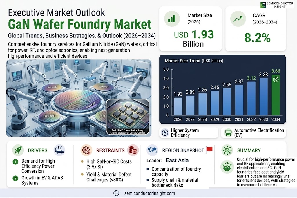
The global GaN Wafer Foundry Market size was valued at US$ 1.78 billion in 2024 and is projected to reach US$ 3.12 billion by 2032, at a CAGR of 8.2% during the forecast period 2025-2032. This growth trajectory reflects the increasing adoption of gallium nitride (GaN) technology across power electronics and radio frequency applications.
GaN wafer foundries specialize in manufacturing semiconductor wafers using gallium nitride, a wide bandgap material offering superior performance over traditional silicon in high-power, high-frequency applications. These foundries enable the production of advanced power devices, RF components, and optoelectronic systems through two primary business models: pure-play foundries that manufacture for third parties and IDM (Integrated Device Manufacturer) foundries that design and produce their own GaN devices.
The market expansion is being driven by multiple factors including growing demand for energy-efficient power electronics, adoption in 5G infrastructure, and increasing electric vehicle production. While consumer electronics currently dominate application segments, industrial and automotive sectors are showing the fastest growth rates. Recent developments include TSMC’s expansion of GaN-on-Silicon production capacity and Samsung Foundry’s introduction of 150mm GaN process technology in 2023. Other key players like UMC and GlobalFoundries are also ramping up GaN production capabilities to meet the surging demand.
MARKET DYNAMICS
MARKET DRIVERS
Expansion of 5G and Electric Vehicle Ecosystems to Accelerate GaN Adoption
The global transition to 5G networks is creating unprecedented demand for gallium nitride (GaN) wafer foundry services, with the compound semiconductor demonstrating superior performance in RF power amplifiers and mobile infrastructure. 5G base station deployments are projected to exceed 7 million units globally by 2025, requiring energy-efficient GaN-based power electronics that can operate at higher frequencies and temperatures than traditional silicon. This technological shift is prompting foundries to expand GaN-on-SiC and GaN-on-Si production capabilities. Leading semiconductor manufacturers are actively retooling facilities – for instance, a major Taiwanese foundry recently dedicated an entire 8-inch wafer line to GaN production to meet surging 5G component demand.
Automotive Electrification Fuelling GaN Foundry Expansion
The automotive industry’s rapid electrification is transforming the GaN wafer foundry landscape. Electric vehicle production is forecast to grow at a 29% CAGR through 2030, creating massive demand for GaN-based power electronics in onboard chargers, DC-DC converters, and traction inverters. GaN’s ability to deliver 40% higher efficiency than silicon in automotive applications is driving major investments – with several leading foundries announcing capacity expansions specifically for automotive-grade GaN wafers. Automotive OEMs are increasingly collaborating with foundries to develop qualified processes, as evidenced by recent long-term supply agreements between European automakers and Asian GaN foundry specialists.
The defense and aerospace sectors are also contributing to market expansion, with GaN emerging as the material of choice for next-generation radar systems and satellite communications. Government investments in military modernization programs worldwide are creating new opportunities for specialized GaN foundries capable of meeting stringent reliability requirements.
MARKET RESTRAINTS
High Production Costs and Yield Challenges Limit Market Penetration
Despite its performance advantages, GaN wafer production faces significant cost barriers that restrain wider adoption. Current GaN-on-SiC wafer costs remain 3-5 times higher than equivalent silicon wafers, primarily due to expensive substrates and complex epitaxial growth processes. Yield rates for power GaN devices currently average below 80% across the industry, compared to over 95% for mature silicon power MOSFETs. These cost differentials make GaN less competitive in price-sensitive applications, particularly in consumer electronics markets where silicon still dominates.
Material defect densities remain a persistent challenge, with dislocation densities in commercial GaN wafers still orders of magnitude higher than in silicon. Several major foundries have delayed volume production timelines due to difficulties in achieving consistent device performance across entire wafers. The industry is actively developing new defect reduction techniques, but widespread yield improvements will require several more years of process refinement.
MARKET CHALLENGES
Supply Chain Vulnerabilities and Geopolitical Tensions Create Market Uncertainty
The GaN wafer foundry sector faces mounting challenges from concentrated supply chains and geopolitical instability. Over 75% of global GaN epitaxial wafer capacity is currently concentrated in East Asia, creating significant supply chain risks as trade tensions escalate. Recent export controls on advanced semiconductor technologies have introduced new uncertainties for foundries operating in affected regions.
The industry also faces materials bottlenecks, with quality GaN substrates remaining difficult to source at scale. Several major substrate suppliers have announced capacity expansions, but rapid demand growth threatens to outpace supply improvements. Foundries are increasingly pursuing vertical integration strategies, with some acquiring substrate manufacturers or developing alternative material solutions to secure supply.
MARKET OPPORTUNITIES
Emerging HPC and Data Center Applications Open New Frontiers
The rapid growth of artificial intelligence and hyperscale computing is creating exciting opportunities for GaN wafer foundries. Data center power consumption is projected to exceed 1,000 TWh annually by 2030, driving demand for ultra-efficient power conversion solutions. GaN is gaining traction in rack-level power delivery systems, with major cloud providers actively evaluating GaN-based power supplies that can reduce energy losses by up to 30%.
Foundries are also exploring GaN applications in cutting-edge computing architectures. Several research initiatives are demonstrating GaN’s potential for monolithic 3D integration and neuromorphic computing applications. While these applications remain in early stages, they represent significant long-term growth avenues for advanced GaN foundry services.
Government Incentives and Regional Diversification Offer Growth Pathways
Global semiconductor localization initiatives present substantial opportunities for GaN foundry expansion. The CHIPS Act in the United States has allocated over $2 billion specifically for compound semiconductor manufacturing, prompting multiple new GaN foundry projects in North America. Similar programs in Europe and Asia are accelerating regional capacity development, reducing reliance on geographically concentrated supply chains.
These government-backed initiatives are enabling new market entrants and technology transitions. Several IDM companies are converting older silicon fabs to GaN production with government support, while pure-play foundries are establishing dedicated GaN lines to serve growing regional demand. This geographical diversification is expected to strengthen overall market resilience while creating new business opportunities throughout the value chain.
GaN WAFER FOUNDRY MARKET TRENDS
5G and Power Electronics Expansion Driving GaN Wafer Demand
The global GaN wafer foundry market is experiencing robust growth, primarily fueled by the rapid adoption of 5G technologies and the increasing demand for efficient power electronics. Gallium Nitride (GaN) semiconductors outperform traditional silicon-based solutions in high-frequency, high-power applications, offering superior thermal conductivity and energy efficiency. The market, valued at approximately $1.2 billion in 2024, is projected to expand at a CAGR of 20-25% through 2032, reflecting strong industry momentum. Foundries specializing in GaN production are scaling capacities to meet the surging demand from telecom infrastructure providers and electric vehicle manufacturers, who require advanced power conversion solutions.
Other Trends
Automotive Industry Electrification
The automotive sector’s accelerating shift toward electrification is significantly boosting GaN wafer adoption. With major automakers targeting 30-40% EV production shares by 2030, GaN-based power modules are becoming essential for onboard chargers, DC-DC converters, and traction inverters. These components benefit from GaN’s ability to operate at higher voltages and temperatures while reducing system weight by up to 50% compared to silicon alternatives. The automotive GaN market segment is expected to grow at nearly 35% CAGR as manufacturers prioritize range extension and fast-charging capabilities in next-generation vehicles.
Defense and Aerospace Applications
Growing defense budgets worldwide are creating new opportunities for radiation-hardened GaN solutions in military communication systems and radar applications. Countries are allocating 15-20% of their annual defense spending to modernize electronic warfare capabilities, where GaN’s power density advantages enable compact, high-performance RF components. The U.S. Department of Defense has identified GaN as a critical technology, with several multi-million dollar contracts awarded to foundries developing next-generation defense-focused GaN wafers in 2023-2024.
GaN Wafer Foundry Market Competitive Landscape
Key Industry Players
Manufacturers Accelerate GaN Technology Investments to Capitalize on Emerging Power Electronics Demand
The GaN wafer foundry market exhibits a moderately consolidated structure, with both integrated device manufacturers (IDMs) and pure-play foundries competing aggressively. TSMC (Taiwan Semiconductor Manufacturing Company) leads the market with over 35% revenue share in 2024, leveraging its advanced 6-inch and 8-inch GaN-on-Si wafer production lines serving major fabless semiconductor companies. The company recently announced a $3.5 billion expansion of its GaN production capacity to meet surging demand from EV and 5G infrastructure markets.
Samsung Foundry has emerged as a strong second player with 22% market share, focusing on high-power GaN solutions for automotive and industrial applications. Their recent partnership with Infineon Technologies aims to develop next-generation GaN power devices, combining Samsung’s manufacturing scale with Infineon’s system expertise. Meanwhile, United Microelectronics Corporation (UMC) holds approximately 15% share through its specialized GaN-on-SiC offerings for RF and power applications.
The competitive intensity is increasing as Chinese players like Sanan Optoelectronics (SANAN) and SMIC aggressively expand their GaN capabilities. SANAN invested $2.1 billion in 2023 to build the world’s largest vertical GaN supply chain, while SMIC is leveraging government subsidies to catch up in GaN-on-silicon technology. These developments are reshaping pricing dynamics across the industry.
Strategic collaborations are becoming critical differentiators – GlobalFoundries recently partnered with GaN device startup Navitas Semiconductor to co-develop power ICs, while VIS (Vanguard International Semiconductor) acquired GaN specialist Episil Technologies to strengthen its position in the Asia-Pacific market.
List of Major GaN Wafer Foundry Companies
- TSMC (Taiwan)
- Samsung Foundry (South Korea)
- United Microelectronics Corporation (UMC) (Taiwan)
- Sanan Optoelectronics (SANAN) (China)
- SixPoint Materials (U.S.)
- GlobalFoundries (U.S.)
- Semiconductor Manufacturing International Corporation (SMIC) (China)
- Powerchip Semiconductor Manufacturing Corporation (PSMC) (Taiwan)
- Vanguard International Semiconductor (VIS) (Taiwan)
- Global Communication Semiconductors (GCS) (U.S.)
Segment Analysis:
By Type
Pure-play Foundry Segment Leads Due to Specialization in GaN Fabrication
The market is segmented based on type into:
- Pure-play Foundry
- Subtypes: 150mm, 200mm, and others
- IDM Foundry
- Subtypes: Vertical integration, hybrid models
By Application
Power Electronics to Remain Primary Application Segment
The market is segmented based on application into:
- Consumer Electronics
- Subtypes: Power adapters, fast chargers
- Industrial
- Automotive
- Subtypes: EV charging, power modules
- High Performance Computing
- Others
By Node Size
Larger Wafer Sizes Gaining Traction for Cost Efficiency
The market is segmented based on node size:
- 150mm
- 200mm
- Others (including emerging 300mm)
By Substrate Technology
Silicon Substrates Lead Due to Cost Advantages
The market is segmented based on substrate technology:
- Silicon-based GaN
- SiC-based GaN
- Sapphire-based GaN
- Others
Regional Analysis: GaN Wafer Foundry Market
North America
The North American GaN wafer foundry market is driven by strong demand from the defense, automotive, and telecommunications sectors, particularly in the U.S. Government investments in 5G infrastructure and wide-bandgap semiconductor adoption are key growth catalysts. The region benefits from a robust semiconductor supply chain and R&D ecosystem, with companies like GlobalFoundries and TSMC Arizona expanding their GaN capabilities. However, reliance on Asian supply chains and high production costs remain challenges. The U.S. CHIPS Act, allocating $52 billion for semiconductor manufacturing, is expected to further boost domestic GaN wafer production and reduce import dependency.
Europe
Europe’s GaN wafer foundry market is growing steadily, supported by stringent energy efficiency regulations and investments in next-gen power electronics. Countries like Germany and France lead in research collaborations between universities and industry players, focusing on automotive and industrial applications. The EU’s Horizon Europe program funds GaN-based projects to enhance energy-efficient technologies. Despite this, the region trails behind Asia in fab capacity and faces competition from established Asian foundries. Partnerships with pure-play foundries like TSMC and UMC are critical to scaling production.
Asia-Pacific
Asia-Pacific dominates the GaN wafer foundry market, accounting for the largest share due to China’s aggressive semiconductor policies and Japan’s leadership in materials science. Taiwan’s TSMC and UMC are global leaders in GaN manufacturing, while China’s SANAN and SMIC are rapidly expanding capacities to reduce reliance on foreign suppliers. India is emerging as a manufacturing hub with state-backed initiatives like the Semiconductor Mission. High-volume production, competitive pricing, and growing 5G and EV adoption sustain the region’s dominance, though geopolitical tensions and IP concerns pose risks.
South America
South America’s GaN wafer foundry market is in early stages, with Brazil and Argentina showing nascent interest in power electronics and renewables. The lack of advanced semiconductor infrastructure and limited government support hinder growth. Most demand is met through imports, particularly from Asia. However, initiatives like Brazil’s National Semiconductor Policy aim to foster local R&D. Long-term potential lies in energy and industrial applications, but progress will likely remain slow due to economic instability and funding gaps.
Middle East & Africa
This region’s market is emerging, with the UAE, Saudi Arabia, and Israel investing in semiconductor ecosystems as part of broader economic diversification plans. Israel’s GaN-on-silicon expertise and partnerships with firms like Tower Semiconductor provide a foundation for niche applications. However, limited local demand and high dependence on imports constrain expansion. Future growth may hinge on renewable energy projects and collaborations with global foundries, though infrastructural deficits and funding challenges persist.
Report Scope
This market research report provides a comprehensive analysis of the global and regional GaN Wafer Foundry markets, covering the forecast period 2025–2032. It offers detailed insights into market dynamics, technological advancements, competitive landscape, and key trends shaping the industry.
Key focus areas of the report include:
- Market Size & Forecast: Historical data and future projections for revenue, unit shipments, and market value across major regions and segments. The global GaN Wafer Foundry market was valued at US$ 1.78 billion in 2024 and is projected to reach US$ 3.12 billion by 2032.
- Segmentation Analysis: Detailed breakdown by product type (Pure-play Foundry, IDM Foundry), application (Consumer Electronics, Industrial, Automotive, High Performance Computing, Others), and end-user industry to identify high-growth segments and investment opportunities.
- Regional Outlook: Insights into market performance across North America, Europe, Asia-Pacific, Latin America, and the Middle East & Africa, including country-level analysis where relevant. Asia-Pacific dominates the market due to strong semiconductor manufacturing presence.
- Competitive Landscape: Profiles of leading market participants including TSMC, Samsung Foundry, UMC, SANAN, and GlobalFoundries, including their product offerings, R&D focus, manufacturing capacity, and recent developments.
- Technology Trends & Innovation: Assessment of emerging GaN fabrication technologies, integration with advanced packaging solutions, and evolving industry standards for power electronics.
- Market Drivers & Restraints: Evaluation of factors driving market growth including demand for efficient power devices, along with challenges such as high production costs and supply chain constraints.
- Stakeholder Analysis: Insights for semiconductor manufacturers, fabless companies, system integrators, investors, and policymakers regarding the evolving GaN ecosystem and strategic opportunities.
Primary and secondary research methods are employed, including interviews with industry experts, data from verified sources, and real-time market intelligence to ensure the accuracy and reliability of the insights presented.
FREQUENTLY ASKED QUESTIONS:
What is the current market size of Global GaN Wafer Foundry Market?
-> GaN Wafer Foundry Market size was valued at US$ 1.78 billion in 2024 and is projected to reach US$ 3.12 billion by 2032, at a CAGR of 8.2% during the forecast period 2025-2032.
Which key companies operate in Global GaN Wafer Foundry Market?
-> Key players include TSMC, Samsung Foundry, UMC, SANAN, SixPoint Materials, GlobalFoundries, SMIC, PSMC, VIS, and GCS.
What are the key growth drivers?
-> Key growth drivers include rising demand for power-efficient devices, expansion of 5G infrastructure, and increasing adoption in automotive and industrial applications.
Which region dominates the market?
-> Asia-Pacific is the dominant market, accounting for the largest share due to strong semiconductor manufacturing capabilities in Taiwan, China, and South Korea.
What are the emerging trends?
-> Emerging trends include development of 8-inch GaN wafers, integration with SiC technology, and increasing focus on RF power applications.

Get Sample Report PDF for Exclusive Insights
Report Sample Includes
- Table of Contents
- List of Tables & Figures
- Charts, Research Methodology, and more...
 Download Sample Report PDF