GaN Inspection and Metrology Equipment Market Overview
Gallium nitride (GaN) is used as the wide band gap material for next generation power semiconductors and high frequency devices. The GaN wafer inspection market is expected to grow significantly, driven by advancements in inspection technologies and the increasing demand for high-performance GaN-based devices. Innovations in automated inspection systems, AI, and machine learning will further enhance the efficiency and accuracy of wafer inspections, reducing manufacturing costs and improving yield rates.
This report provides a deep insight into the global GaN Inspection and Metrology Equipment market covering all its essential aspects. This ranges from a macro overview of the market to micro details of the market size, competitive landscape, development trend, niche market, key market drivers and challenges, SWOT analysis, value chain analysis, etc.
The analysis helps the reader to shape the competition within the industries and strategies for the competitive environment to enhance the potential profit. Furthermore, it provides a simple framework for evaluating and accessing the position of the business organization. The report structure also focuses on the competitive landscape of the Global GaN Inspection and Metrology Equipment Market, this report introduces in detail the market share, market performance, product situation, operation situation, etc. of the main players, which helps the readers in the industry to identify the main competitors and deeply understand the competition pattern of the market.
In a word, this report is a must-read for industry players, investors, researchers, consultants, business strategists, and all those who have any kind of stake or are planning to foray into the GaN Inspection and Metrology Equipment market in any manner.
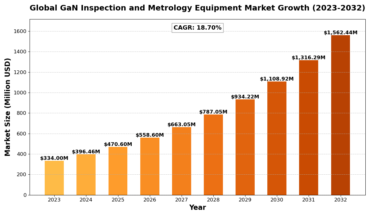
GaN Inspection and Metrology Equipment Market Analysis:
The global GaN Inspection and Metrology Equipment market size was estimated at USD 334 million in 2023 and is projected to reach USD 1562.44 million by 2032, exhibiting a CAGR of 18.70% during the forecast period.
North America GaN Inspection and Metrology Equipment market size was estimated at USD 117.17 million in 2023, at a CAGR of 16.03% during the forecast period of 2025 through 2032.
GaN Inspection and Metrology Equipment Key Market Trends :
-
Growing 5G and RF Semiconductor Demand
The expansion of 5G networks is accelerating the need for GaN-based semiconductors, increasing the demand for accurate inspection and metrology solutions. -
Advancements in Automated Optical Inspection (AOI)
AI-driven AOI systems are enhancing defect detection in GaN wafers, reducing production errors and improving yield rates. -
Rising Adoption of GaN in Power Electronics
GaN is increasingly used in power conversion systems, requiring precise inspection tools to maintain high performance and efficiency. -
Integration of AI and Machine Learning
Smart inspection systems with AI-driven analytics are improving the accuracy and speed of GaN wafer defect detection and quality control. -
Expansion of GaN in Automotive Applications
GaN-based components are gaining traction in electric vehicles (EVs) and advanced driver-assistance systems (ADAS), fueling the demand for metrology equipment.
GaN Inspection and Metrology Equipment Market Regional Analysis :

-
North America:
Strong demand driven by EVs, 5G infrastructure, and renewable energy, with the U.S. leading the market.
-
Europe:
Growth fueled by automotive electrification, renewable energy, and strong regulatory support, with Germany as a key player.
-
Asia-Pacific:
Dominates the market due to large-scale manufacturing in China and Japan, with growing demand from EVs, 5G, and semiconductors.
-
South America:
Emerging market, driven by renewable energy and EV adoption, with Brazil leading growth.
-
Middle East & Africa:
Gradual growth, mainly due to investments in renewable energy and EV infrastructure, with Saudi Arabia and UAE as key contributors.
GaN Inspection and Metrology Equipment Market Segmentation :
The research report includes specific segments by region (country), manufacturers, Type, and Application. Market segmentation creates subsets of a market based on product type, end-user or application, Geographic, and other factors. By understanding the market segments, the decision-maker can leverage this targeting in the product, sales, and marketing strategies. Market segments can power your product development cycles by informing how you create product offerings for different segments.
Key Company
- KLA Corporation
- Lasertec
- Nanotronics
- TASMIT
- Inc. (Toray Engineering)
- Bruker
- LAZIN CO.,LTD
- EtaMax
- Screen
- Tokyo Electron Ltd. (TEL)
- confovis GmbH
- Angkun Vision (Beijing) Technology
- Shenzhen Glint Vision
- Hitachi High-Tech
- Onto Innovation
Market Segmentation (by Type)
- GaN Defect Inspection Equipment
- GaN Metrology Equipment
Market Segmentation (by Application)
- GaN RF
- GaN Power
- HB GaN LED
Drivers
-
Increasing Use of GaN in High-Power Applications
The demand for GaN-based semiconductors in power electronics, RF devices, and satellite communication is driving market growth. -
Rising Focus on Quality Control
Manufacturers are investing in advanced metrology solutions to enhance defect detection and ensure the reliability of GaN-based devices. -
Technological Advancements in Inspection Equipment
Innovations in optical, X-ray, and electron microscopy inspection tools are improving measurement accuracy and efficiency.
Restraints
-
High Cost of Advanced Metrology Equipment
The expensive nature of precision inspection systems limits adoption, particularly among small and medium-sized semiconductor manufacturers. -
Complexity of GaN Material Analysis
GaN wafer inspection requires specialized techniques, making the process more challenging compared to silicon-based semiconductor metrology. -
Limited Standardization in GaN Manufacturing
The lack of standardized processes in GaN fabrication creates inconsistencies in inspection and metrology requirements.
Opportunities
-
Emerging Applications in EVs and Renewable Energy
The growing use of GaN in EV charging stations and renewable energy systems presents new opportunities for metrology equipment manufacturers. -
Development of AI-Powered Inspection Solutions
AI-driven defect detection and predictive analytics are improving semiconductor inspection efficiency and reducing manufacturing defects. -
Expansion of Semiconductor Manufacturing Facilities
Increasing investments in semiconductor fabs, particularly in Asia-Pacific, are boosting demand for advanced GaN inspection equipment.
Challenges
-
Stringent Quality Requirements
GaN-based devices require high precision in defect detection, making quality control processes more demanding. -
Supply Chain Disruptions
Fluctuations in the supply of GaN wafers and semiconductor components impact the availability of inspection and metrology equipment. -
Integration with Existing Semiconductor Ecosystems
Ensuring compatibility between GaN inspection tools and traditional semiconductor manufacturing processes remains a key challenge.
Key Benefits of This Market Research:
- Industry drivers, restraints, and opportunities covered in the study
- Neutral perspective on the market performance
- Recent industry trends and developments
- Competitive landscape & strategies of key players
- Potential & niche segments and regions exhibiting promising growth covered
- Historical, current, and projected market size, in terms of value
- In-depth analysis of the GaN Inspection and Metrology Equipment Market
- Overview of the regional outlook of the GaN Inspection and Metrology Equipment Market:
Key Reasons to Buy this Report:
- Access to date statistics compiled by our researchers. These provide you with historical and forecast data, which is analyzed to tell you why your market is set to change
- This enables you to anticipate market changes to remain ahead of your competitors
- You will be able to copy data from the Excel spreadsheet straight into your marketing plans, business presentations, or other strategic documents
- The concise analysis, clear graph, and table format will enable you to pinpoint the information you require quickly
- Provision of market value data for each segment and sub-segment
- Indicates the region and segment that is expected to witness the fastest growth as well as to dominate the market
- Provides insight into the market through Value Chain
- Market dynamics scenario, along with growth opportunities of the market in the years to come
- 6-month post-sales analyst support
Customization of the Report
In case of any queries or customization requirements, please connect with our sales team, who will ensure that your requirements are met.
FAQs
Q: What are the key driving factors and opportunities in the GaN inspection and metrology equipment market?
A: The market is driven by the growing adoption of GaN in power electronics, 5G, and automotive applications. Opportunities include AI-driven inspection solutions and expanding semiconductor production facilities.
Q: Which region is projected to have the largest market share?
A: Asia-Pacific is expected to dominate the market due to its strong semiconductor manufacturing base and increasing demand for GaN-based devices.
Q: Who are the top players in the global GaN inspection and metrology equipment market?
A: Leading companies include KLA Corporation, Onto Innovation, Hitachi High-Tech, Bruker Corporation, and Camtek Ltd., which are driving advancements in inspection technologies.
Q: What are the latest technological advancements in the industry?
A: Innovations include AI-powered metrology systems, automated optical inspection (AOI) enhancements, and improved X-ray and electron microscopy techniques.
Q: What is the current size of the global GaN inspection and metrology equipment market?
A: The market is witnessing steady growth, with projections indicating significant expansion from 2025 to 2032 due to rising demand for GaN-based semiconductors.

Get Sample Report PDF for Exclusive Insights
Report Sample Includes
- Table of Contents
- List of Tables & Figures
- Charts, Research Methodology, and more...