GaN HEMT Epitaxial Wafer Market Overview
GaN HEMT epitaxial wafer is a multilayer film grown epitaxially on a substrate, which usually includes a nucleation layer, a transition layer, a buffer layer, a channel layer, a barrier layer, a cap layer, and a passivation layer from bottom to top. Using gallium nitride (GaN) HEMT epiwafer brings various benefits for the next generation high frequency and high power devices. At the device level, GaN devices exceed limitations of the conventional Si devices. GaN devices can achieve very high-power efficiency, which accordingly reduces their size and lower power consumption, consequently that of their final products.
This report provides a deep insight into the global GaN HEMT Epitaxial Wafer market covering all its essential aspects. This ranges from a macro overview of the market to micro details of the market size, competitive landscape, development trend, niche market, key market drivers and challenges, SWOT analysis, value chain analysis, etc.
The analysis helps the reader to shape the competition within the industries and strategies for the competitive environment to enhance the potential profit. Furthermore, it provides a simple framework for evaluating and accessing the position of the business organization. The report structure also focuses on the competitive landscape of the Global GaN HEMT Epitaxial Wafer Market, this report introduces in detail the market share, market performance, product situation, operation situation, etc. of the main players, which helps the readers in the industry to identify the main competitors and deeply understand the competition pattern of the market.
In a word, this report is a must-read for industry players, investors, researchers, consultants, business strategists, and all those who have any kind of stake or are planning to foray into the GaN HEMT Epitaxial Wafer market in any manner.
GaN HEMT Epitaxial Wafer Market Analysis:
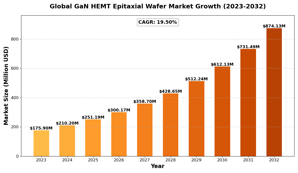
The global GaN HEMT Epitaxial Wafer Market size was estimated at USD 175.90 million in 2023 and is projected to reach USD 874.13 million by 2032, exhibiting a CAGR of 19.50% during the forecast period.
North America GaN HEMT Epitaxial Wafer market size was estimated at USD 62.44 million in 2023, at a CAGR of 16.71% during the forecast period of 2025 through 2032.
GaN HEMT Epitaxial Wafer Key Market Trends :
- Growing Adoption in 5G Infrastructure: GaN HEMT technology is becoming essential for 5G applications due to its high frequency, efficiency, and power-handling capabilities.
- Advancements in Power Electronics: Increasing demand for high-performance power electronics in automotive, aerospace, and consumer electronics is driving the market growth.
- Shift Towards GaN-on-Si Technology: The industry is witnessing a rise in GaN-on-Si solutions due to their cost-effectiveness and compatibility with existing silicon manufacturing processes.
- Rising Investments in R&D: Companies are focusing on improving GaN HEMT wafer fabrication techniques to enhance performance and reduce costs.
- Expansion of Semiconductor Manufacturing in Asia-Pacific: The Asia-Pacific region is emerging as a key hub for semiconductor production, boosting the demand for GaN HEMT wafers.
GaN HEMT Epitaxial Wafer Market Regional Analysis :

-
North America:
Strong demand driven by EVs, 5G infrastructure, and renewable energy, with the U.S. leading the market.
-
Europe:
Growth fueled by automotive electrification, renewable energy, and strong regulatory support, with Germany as a key player.
-
Asia-Pacific:
Dominates the market due to large-scale manufacturing in China and Japan, with growing demand from EVs, 5G, and semiconductors.
-
South America:
Emerging market, driven by renewable energy and EV adoption, with Brazil leading growth.
-
Middle East & Africa:
Gradual growth, mainly due to investments in renewable energy and EV infrastructure, with Saudi Arabia and UAE as key contributors.
GaN HEMT Epitaxial Wafer Market Segmentation :
The research report includes specific segments by region (country), manufacturers, Type, and Application. Market segmentation creates subsets of a market based on product type, end-user or application, Geographic, and other factors. By understanding the market segments, the decision-maker can leverage this targeting in the product, sales, and marketing strategies. Market segments can power your product development cycles by informing how you create product offerings for different segments.
Key Company
- Wolfspeed
- Inc
- IQE
- Soitec (EpiGaN)
- Transphorm Inc.
- Sumitomo Chemical (SCIOCS)
- NTT Advanced Technology (NTT-AT)
- DOWA Electronics Materials
- BTOZ
- Episil-Precision Inc
- Epistar Corp.
- CETC 13
- CETC 55
- Enkris Semiconductor Inc
- Innoscience
- Runxin Microelectronics
- CorEnergy
- Suzhou Nanowin Science and Technology
- Qingdao Cohenius Microelectronics
- Shaanxi Yuteng Electronic Technology
- Dynax Semiconductor
- Sanan Optoelectronics
Market Segmentation (by Type)
- GaN-on-SiC
- GaN-on-Si
- GaN-on-Sapphire
- GaN on GaN Others
Market Segmentation (by Application)
- GaN HEMT RF Devices
- GaN HEMT Power Devices
Drivers
- High Demand for Energy-Efficient Devices: GaN HEMT technology offers superior efficiency, reducing energy consumption in power electronics applications.
- Growth of 5G and Wireless Communication: Increased deployment of 5G networks is driving demand for GaN-based RF devices.
- Rise in Electric Vehicles (EVs): GaN HEMT wafers are crucial in EV powertrains and charging systems, supporting market expansion.
Restraints
- High Manufacturing Costs: The production cost of GaN HEMT epitaxial wafers remains high compared to silicon alternatives.
- Complex Fabrication Process: The intricate manufacturing process poses challenges in scaling up production.
- Limited Availability of Raw Materials: The supply chain for GaN materials is not as mature as that of silicon, causing supply constraints.
Opportunities
- Expansion of GaN-on-Si Market: Cost-effective GaN-on-Si technology is opening new growth avenues in the industry.
- Government Initiatives for Semiconductor Development: Increasing investments and incentives in semiconductor manufacturing are benefiting GaN technology.
- Emerging Applications in Aerospace & Defense: GaN-based RF and power devices are gaining traction in military and space applications.
Challenges
- Competition from Silicon and SiC Technologies: GaN faces competition from silicon and SiC in various power applications.
- Technical Challenges in Mass Production: Achieving uniform wafer quality and reliability remains a hurdle.
- Limited Standardization: Lack of industry-wide standardization affects GaN device adoption across different applications.
Key Benefits of This Market Research:
- Industry drivers, restraints, and opportunities covered in the study
- Neutral perspective on the market performance
- Recent industry trends and developments
- Competitive landscape & strategies of key players
- Potential & niche segments and regions exhibiting promising growth covered
- Historical, current, and projected market size, in terms of value
- In-depth analysis of the GaN HEMT Epitaxial Wafer Market
- Overview of the regional outlook of the GaN HEMT Epitaxial Wafer Market:
Key Reasons to Buy this Report:
- Access to date statistics compiled by our researchers. These provide you with historical and forecast data, which is analyzed to tell you why your market is set to change
- This enables you to anticipate market changes to remain ahead of your competitors
- You will be able to copy data from the Excel spreadsheet straight into your marketing plans, business presentations, or other strategic documents
- The concise analysis, clear graph, and table format will enable you to pinpoint the information you require quickly
- Provision of market value data for each segment and sub-segment
- Indicates the region and segment that is expected to witness the fastest growth as well as to dominate the market
- Provides insight into the market through Value Chain
- Market dynamics scenario, along with growth opportunities of the market in the years to come
- 6-month post-sales analyst support
Customization of the Report
In case of any queries or customization requirements, please connect with our sales team, who will ensure that your requirements are met.
FAQs
Q: What are the key driving factors and opportunities in the GaN HEMT Epitaxial Wafer market?
A: The key driving factors include the rising demand for energy-efficient devices, growth in 5G infrastructure, and the expansion of electric vehicles (EVs). Opportunities lie in GaN-on-Si technology advancements, government support for semiconductor development, and growing aerospace applications.
Q: Which region is projected to have the largest market share?
A: Asia-Pacific is expected to dominate the market due to increasing semiconductor manufacturing, strong government support, and rising adoption of GaN technology in power and RF applications.
Q: Who are the top players in the global GaN HEMT Epitaxial Wafer market?
A: Leading players include Wolfspeed Inc, IQE, Soitec (EpiGaN), Transphorm Inc., Sumitomo Chemical (SCIOCS), and Enkris Semiconductor Inc.
Q: What are the latest technological advancements in the industry?
A: Recent advancements include GaN-on-Si technology for cost reduction, improved fabrication techniques for higher efficiency, and innovations in GaN-based RF and power devices for enhanced performance.
Q: What is the current size of the global GaN HEMT Epitaxial Wafer market?
A: The market was valued at USD 175.90 million in 2023 and is projected to reach USD 874.13 million by 2032, growing at a CAGR of 19.50% during the forecast period.

Get Sample Report PDF for Exclusive Insights
Report Sample Includes
- Table of Contents
- List of Tables & Figures
- Charts, Research Methodology, and more...