Market Insights
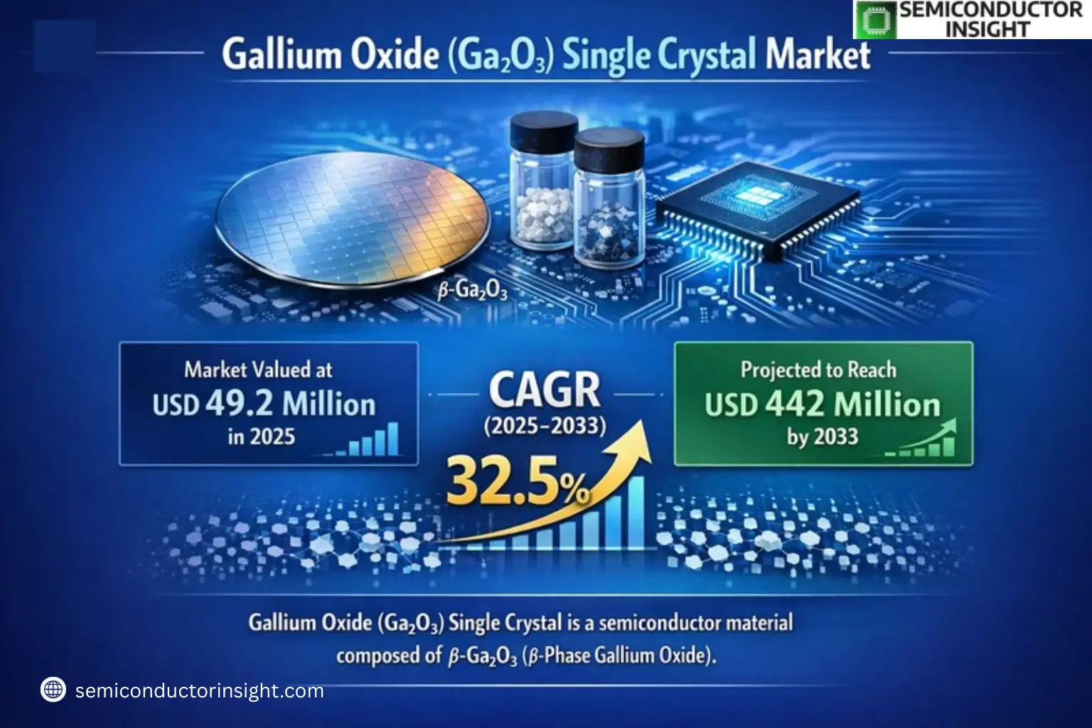
Global ?-Gallium Oxide(Ga2O3) Single Crystal Market was valued at USD 49.2 million in 2025 and is projected to reach USD 442 million by 2033, exhibiting a CAGR of 32.5% during the forecast period.
?-Gallium Oxide(Ga2O3) Single Crystal is a semiconductor material composed of β-phase gallium oxide (β-Ga2O3). It is characterized by its ultra-wide bandgap of approximately 4.9 eV, high breakdown electric field strength (8 MV/cm), and excellent ultraviolet transmittance. These properties make it ideal for high-power, high-voltage, and UV-sensitive applications. Compared to traditional semiconductors like silicon (Si), silicon carbide (SiC), and gallium nitride (GaN), β-Ga2O3 offers superior performance in power efficiency and voltage resistance, positioning it as a critical material for next-generation electronic devices.
The market growth is driven by increasing demand for energy-efficient power electronics in sectors such as electric vehicles, renewable energy systems, and 5G infrastructure. Additionally, advancements in crystal growth techniques, particularly the development of larger wafer sizes like 6-inch substrates, are enhancing production scalability. Key players such as Novel Crystal Technology and Kyma Technologies are investing in R&D to overcome challenges related to defect control and epitaxial processes, further accelerating commercialization efforts.
MARKET DRIVERS
Growing Demand in Power Electronics Applications
?-Gallium Oxide(Ga2O3) Single Crystal Market is experiencing significant growth due to its superior properties in high-power electronic devices. With a bandgap of 4.8 eV, Ga2O3 enables higher breakdown voltages and efficiency compared to silicon carbide (SiC) and gallium nitride (GaN). This makes it ideal for next-generation power devices, particularly in electric vehicles and renewable energy systems.
Advancements in Crystal Growth Technologies
Recent innovations in edge-defined film-fed growth (EFG) and Czochralski methods have improved the production of high-quality β-Ga2O3 single crystals. These advancements reduce production costs while enhancing crystal purity, making Ga2O3 more commercially viable for large-scale applications.
Additionally, increasing R&D investments from semiconductor manufacturers and government initiatives supporting wide-bandgap semiconductor development further accelerate market adoption.
MARKET CHALLENGES
Material Processing Difficulties
The high melting point (1800°C) and thermal conductivity challenges of β-Ga2O3 single crystals present significant manufacturing hurdles. Unlike SiC or GaN, Ga2O3 lacks native substrates, requiring specialized processing techniques that increase production complexity and costs.
Other Challenges
Limited Commercial Infrastructure
The β-Ga2O3 supply chain remains underdeveloped compared to established semiconductors, with few manufacturers capable of producing large-diameter wafers consistently.
MARKET RESTRAINTS
Competition from Established Wide-Bandgap Materials
The widespread adoption of SiC and GaN in power electronics creates strong competition for β-Ga2O3 single crystals. With over 80% market penetration in high-power applications, these mature technologies benefit from established manufacturing ecosystems and proven reliability records.
MARKET OPPORTUNITIES
Expansion in Ultra-High Voltage Applications
β-Ga2O3 single crystals present unparalleled opportunities in >10kV power devices, where their Baliga’s figure of merit exceeds SiC by 10x. This positions Ga2O3 as the optimal material for future smart grid systems and industrial power conversion equipment.
MAIN TITLE HERE (β-Gallium Oxide(Ga2O3) Single Crystal Market) Trends
Ultra-Wide Bandgap Semiconductor Technology Drives Market Growth
?-Gallium Oxide(Ga2O3) Single Crystal Market is witnessing rapid expansion, projected to grow from USD 49.2 million in 2025 to USD 442 million by 2033 at a 32.5% CAGR. This surge is fueled by the material’s superior electrical properties, with 4.9 eV bandgap width and 8 MV/cm breakdown strength, making it ideal for high-power applications. The market is responding to increasing demand from electric vehicles, smart grids, and 5G infrastructure where efficiency at high voltages is critical.
Other Trends
Regional Manufacturing Strategies
Japan leads in heteroepitaxial wafer technology through firms like FLOSFIA, while U.S. development focuses on defense applications. China is accelerating industrialization via policy support for photovoltaic inverters and EV components. Competition is intensifying as these regions invest in 6-inch wafer production to reduce costs.
Technical Challenges and Commercialization Barriers
Material defect control remains a critical bottleneck, with current yields below commercial requirements. The industry must overcome crystal quality and epitaxial process limitations within 3-5 years to achieve mass adoption. Success could position β-Ga2O3 to capture 15-20% of the medium/high voltage power device market currently dominated by SiC and GaN semiconductors.
Emerging Application Sectors
Beyond power electronics, deep ultraviolet detection and aerospace applications are creating new demand vectors. Military systems requiring radiation-hardened components and UV-C disinfection equipment manufacturers are actively evaluating β-Ga2O3 solutions, potentially adding USD 80-100 million to the addressable market by 2030.
COMPETITIVE LANDSCAPE
Key Industry Players
The β-Ga2O3 Crystal Market is Dominated by Specialized Semiconductor Material Providers
?-Gallium Oxide(Ga2O3) Single Crystal Market is currently led by Japanese and American semiconductor material specialists, with Novel Crystal Technology (NCT) and Kyma Technologies establishing early technological advantages. NCT holds approximately 35% market share in substrate production, leveraging its patented edge-defined film-fed growth (EFG) method. The competitive landscape shows a concentrated top tier controlling over 60% of production capacity, with significant R&D focus on 6-inch wafer commercialization to meet power device demand.
Chinese manufacturers are rapidly catching up through government-backed initiatives, with Beijing MIG and CETC making substantial progress in defect control technologies. Meanwhile, startups like Evolusia and FLOSFIA are pioneering cost-effective deposition methods targeting the electric vehicle sector. The market exhibits regional specialization – Japanese firms lead in high-purity substrates, American companies excel in military-grade crystals, while Chinese players focus on scaled production for consumer electronics applications.
List of Key β-Gallium Oxide Single Crystal Companies Profiled
- Novel Crystal Technology
- Kyma Technologies
- Atecom Technology
- Garen Semi
- CETC
- Hangzhou Fujia
- Beijing MIG
- Gao Semi
- CSW Xiamen
- Evolusia
- FLOSFIA
- NGK Insulators
- UBE Industries
- Tamura Corporation
- Ohara Corporation
Segment Analysis:
| Segment Category | Sub-Segments | Key Insights |
| By Type |
|
6 Inches
|
| By Application |
|
Automotive
|
| By End User |
|
Semiconductor Manufacturers
|
| By Technology Stage |
|
Prototyping
|
| By Regional Focus |
|
Asia Pacific
|
Regional Analysis: Global ?-Gallium Oxide(Ga2O3) Single Crystal Market
Asia-Pacific
Japan maintains its edge through continuous innovation in bulk crystal growth methods for Ga2O3 substrates. The country’s semiconductor giants collaborate closely with materials researchers to optimize crystal quality for high-voltage applications, particularly in power conversion systems.
Chinese manufacturers are scaling up Ga2O3 production capacities to meet domestic demand while improving crystal size and defect control. Government-backed research programs focus on overcoming technical challenges in epitaxial growth for power device applications.
South Korean electronics conglomerates are integrating Ga2O3 single crystals into next-generation power modules. The nation’s strong fabless ecosystem and advanced packaging capabilities complement its Ga2O3 material development efforts for 5G infrastructure and EV power systems.
Taiwan leverages its semiconductor foundry expertise to develop specialized Ga2O3 device processing techniques. Collaborative projects between research institutes and TSMC aim to commercialize Ga2O3-based power devices while addressing thermal management challenges.
North America
North America demonstrates strong R&D capabilities in Ga2O3 crystal technology, with the U.S. Department of Energy supporting several research initiatives. American firms are pioneering novel doping techniques to enhance Ga2O3 conductivity while academic institutions explore defect engineering solutions. The region sees increasing adoption in defense and aerospace applications where high-voltage operation is critical. Strategic partnerships between materials startups and power electronics manufacturers are accelerating commercialization.
Europe
European research centers are making significant contributions to Ga2O3 crystal growth methodologies, particularly in Germany and the UK. The region focuses on sustainable production processes and recycling solutions for Ga2O3 substrates. Automotive manufacturers are evaluating Ga2O3-based components for next-generation electric vehicle powertrains. EU-funded projects aim to establish standardized testing protocols for Ga2O3 power devices.
Middle East & Africa
The region is emerging as an important consumer of Ga2O3 power devices for renewable energy applications. Investments in solar power infrastructure and grid modernization projects create opportunities for Ga2O3-based high-voltage converters. Limited local production currently exists, but strategic partnerships with Asian suppliers are developing to serve growing regional demand.
South America
Brazil leads Ga2O3 adoption in South America primarily for industrial power conversion applications. The region benefits from technology transfer agreements with North American and Asian partners. While local production remains limited, research institutions are establishing Ga2O3 characterization capabilities to support regional electronics manufacturers.
Report Scope
This market research report provides a comprehensive analysis of the ?-Gallium Oxide(Ga2O3) Single Crystal Market , covering the forecast period 2025–2033. It offers detailed insights into market dynamics, technological advancements, competitive landscape, and key trends shaping the industry.
Key focus areas of the report include:
- Market Overview: The report begins with an overview outlining its current market scenario, key growth indicators, and industry transformation drivers. It discusses macroeconomic factors, demand–supply balance, regulatory landscape, and the strategic role of semiconductors in powering advancements across industries such as automotive, telecommunications, consumer electronics, and industrial automation.
- Market Size & Forecast: Historical data and future projections for revenue, unit shipments, and market value across major regions and segments.
- Segmentation Analysis: Detailed breakdown by product type, technology, application, and end-user industry to identify high-growth segments and investment opportunities.
- Regional Insights: Insights into market performance across North America, Europe, Asia-Pacific, Latin America, and the Middle East & Africa, including country-level analysis where relevant.
- Competitive Landscape: Profiles of leading market participants, including their product offerings, R&D focus, manufacturing capacity, pricing strategies, and recent developments such as mergers, acquisitions, and partnerships.
- Technology Trends & Innovation: Assessment of emerging technologies, integration of AI/IoT, semiconductor design trends, fabrication techniques, and evolving industry standards.
- Market Drivers & Restraints: Evaluation of factors driving market growth along with challenges, supply chain constraints, regulatory issues, and market-entry barriers.
- Stakeholder Insights: Insights for component suppliers, OEMs, system integrators, investors, and policymakers regarding the evolving ecosystem and strategic opportunities.
Primary and secondary research methods are employed, including interviews with industry experts, data from verified sources, and real-time market intelligence to ensure the accuracy and reliability of the insights presented.
FREQUENTLY ASKED QUESTIONS:
What is the current market size of ?-Gallium Oxide(Ga2O3) Single Crystal Market?
-> ?-Gallium Oxide(Ga2O3) Single Crystal Market was valued at USD 49.2 million in 2025 and is projected to reach USD 442 million by 2033, exhibiting a CAGR of 32.5% during the forecast period.
What is the growth rate of ?-Gallium Oxide(Ga2O3) Single Crystal Market?
-> The market is projected to grow at a CAGR of 32.5% during the forecast period (2025-2033).
Which key companies operate in ?-Gallium Oxide(Ga2O3) Single Crystal Market?
-> Key players include Novel Crystal Technology, Kyma Technologies, Atecom Technology, Garen Semi, CETC, Hangzhou Fujia, Beijing MIG, Gao Semi, CSW Xiamen, and Evolusia, among others.
What are the key applications of ?-Gallium Oxide(Ga2O3) Single Crystal?
-> Key applications include high power devices, high voltage resistance components, ultraviolet detectors, automotive electronics, and research applications.
Which region dominates the ?-Gallium Oxide(Ga2O3) Single Crystal market?
-> Asia currently leads the market with strong presence in Japan and China, while North America shows significant growth driven by defense and high-power device applications.

Get Sample Report PDF for Exclusive Insights
Report Sample Includes
- Table of Contents
- List of Tables & Figures
- Charts, Research Methodology, and more...
 Download Sample Report PDF