Gallium Oxide Substrates Market Insights
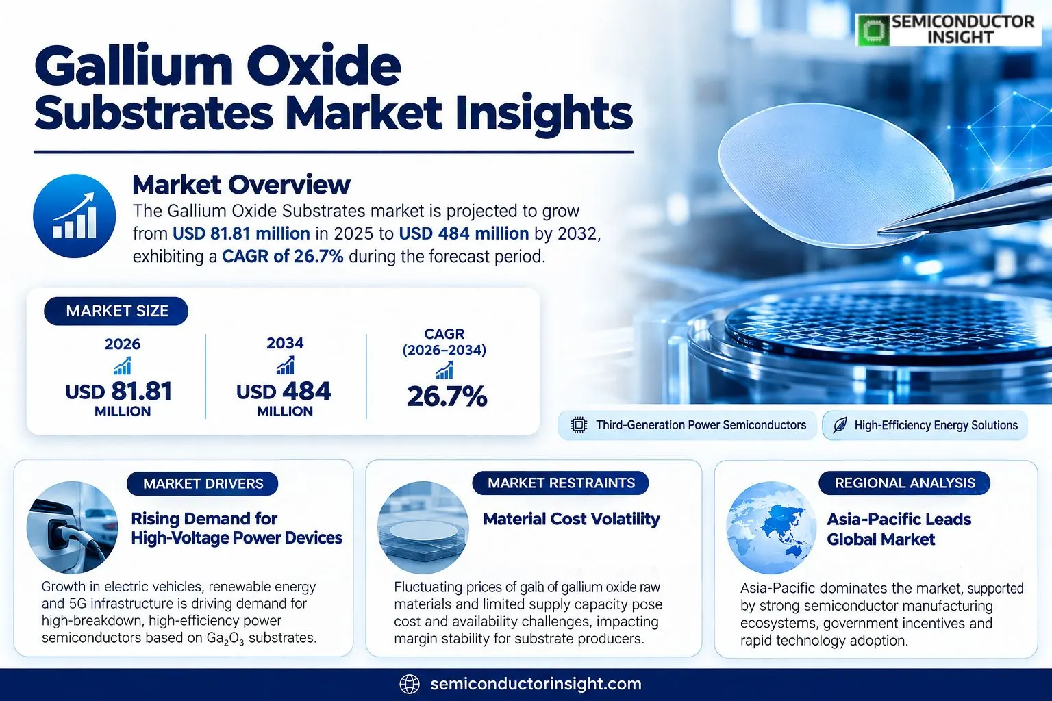
Gallium Oxide Substrates market size was valued at USD 81.81 million in 2025 and is projected to reach USD 484 million by 2032, exhibiting a CAGR of 26.7% during the forecast period.
In 2025, worldwide sales of gallium oxide (GaO) substrates totaled 21,300 pieces with an average selling price of USD 4,200 per piece. These substrates are fabricated from high‑purity gallium oxide (Ga₂O₃), a material noted for its exceptionally high breakdown field strength, wide bandgap (≈4.6‑4.9 eV depending on crystal phase), and robust thermal stability. Such characteristics make GaO substrates attractive for high‑voltage power MOSFETs, RF amplifiers, automotive charging modules, and optoelectronic detection chips. Upstream inputshigh‑purity Ga₂O₃ powder and precious‑metal crucibles (platinum or iridium)represent roughly 58 % of total cost, while downstream power‑electronics and RF‑module manufacturing consume about 72 % of overall consumption.
MARKET DRIVERS
Rising demand for high‑voltage power devices
Gallium Oxide Substrates Market is benefitting from automotive manufacturers’ shift toward electric drivetrains that require converters capable of handling 1.2 kV and above. Designers value the material’s ultra‑wide bandgap, which translates into lower on‑resistance and higher efficiencyattributes that directly reduce battery‑pack heat generation and extend vehicle range.
Advances in substrate manufacturing techniques
Recent refinements in epitaxial growth, particularly metal‑organic chemical vapor deposition, have cut defect densities by roughly 30 % compared with early‑generation processes. This improvement enables manufacturers to achieve yields that approach those of silicon carbide, making large‑area gallium oxide wafers economically viable for mass production.
➤ Industry surveys indicate that customers are willing to pay a 15 % premium for substrates that demonstrate superior breakdown voltage and thermal stability.
When combined, these forces create a feedback loop: higher‑performance devices justify investment in more sophisticated equipment, which in turn drives down per‑unit cost and expands the addressable market for gallium oxide solutions.
MARKET CHALLENGES
Material cost volatility
Gallium oxide raw material prices have surged by over 40 % in the past 18 months, reflecting limited mining capacity and heightened competition from optoelectronic applications. This price swing compresses margins for substrate producers and forces end‑users to reassess cost‑benefit calculations.
Other Challenges
Supply chain constraints
The niche nature of gallium‑oxide feedstock means that a handful of suppliers dominate the market. Disruptionswhether geopolitical or logisticalcan create bottlenecks that delay production schedules for high‑volume automotive contracts.
MARKET RESTRAINTS
Thermal management limitations
Although gallium oxide exhibits excellent electrical characteristics, its thermal conductivity remains lower than that of silicon carbide. Designers therefore must incorporate additional heat‑spreading layers, which can offset some of the efficiency gains and raise overall system cost.
MARKET OPPORTUNITIES
Expansion into automotive power modules
Electric‑vehicle manufacturers are evaluating gallium‑oxide substrates for on‑board chargers that operate at 800 V to 1.2 kV. Successful integration would allow chargers to shrink by up to 25 % while delivering faster charging times. Early adopters could secure a competitive edge by offering vehicles with reduced charging infrastructure costs.
Gallium Oxide Substrates Market Trends
Surging Demand for High‑Voltage Power Devices
Gallium Oxide Substrates Market recorded a revenue of US $81.81 million in 2025, supported by sales of roughly 21,300 pieces at an average selling price of $4,200. The combination of a 45 % gross margin and a production capacity of about 70,000 pieces per year demonstrates a business model that capitalises on the material’s unique electrical characteristicsnamely a breakdown field exceeding 8 MV cm⁻¹ and a bandgap near 4.7 eV. These attributes enable power MOSFETs and RF amplifiers to operate at voltage levels that traditional silicon cannot sustain, prompting automotive OEMs and telecom equipment makers to allocate a larger share of their semiconductor budgets to Ga₂O₃‑based components. The upward trajectory towards a projected US $484 million by 2032 reflects not only incremental price advantages but also a strategic pivot by leading manufacturers toward volume‑scaled fab lines.
Other Trends
Supply‑Chain Cost Structure
Up‑stream inputs dominate the cost profile: high‑purity gallium oxide powder and precious‑metal crucibles (platinum, iridium) together account for roughly 58 % of total expense. Down‑stream consumption, dominated by power‑electronics and RF module assembly, absorbs about 72 % of the overall material usage, indicating that cost‑saving initiatives must focus on both raw‑material sourcing and yield optimisation during wafer fabrication. Companies such as Furuya Metal and Heraeus are expanding their capacity for ultra‑pure powders, while strategic partnerships with crucible suppliers aim to stabilise pricing in the face of fluctuating metal markets. For end‑users, the high gross margin suggests ample room for negotiated pricing, yet the concentration of cost drivers raises the risk of supply disruptions, prompting many OEMs to lock‑in long‑term contracts.
Shift Toward Larger Wafer Sizes and Defect Reduction
Historically, Ga₂O₃ substrates have been limited to 2‑inch and 4‑inch diameters, but recent pilot runs of 6‑inch wafers have demonstrated defect densities below 10⁴ cm⁻², a threshold that makes mass‑production economically viable. This evolution is spurring vertical integration, where crystal growers, substrate processors, and device assemblers coordinate on defect‑control protocols and surface‑treatment chemistries. The move to larger formats not only lowers per‑chip cost but also aligns Ga₂O₃ with the manufacturing footprints of competing SiC and GaN platforms, facilitating a smoother transition for foundries seeking to diversify their power‑semiconductor portfolio. As the industry refines growth‑rate control and adopts advanced Czochralski and Bridgman techniques, the expectation is a measurable drop in the unit price of substrates, thereby widening the addressable market for high‑voltage converters, electric‑vehicle chargers, and space‑qualified RF front‑ends.
COMPETITIVE LANDSCAPEKey Industry Players
Competitive Dynamics of Gallium Oxide Substrate Supply Chain
Novel Crystal Technology dominates the upper tier of the market, leveraging its proprietary Czochralski growth line and a vertically integrated model that spans high‑purity Ga₂O₃ powder sourcing to final wafer processing. Its ability to control crucible material qualityparticularly platinum‑iridium assemblieshas translated into a gross margin well above the industry average, allowing the firm to reinvest in defect‑reduction R&D while expanding capacity toward 6‑inch diameters. The company’s close relationships with downstream power‑electronics OEMs such as Infineon and ROHM reinforce a feedback loop that shapes product specifications and accelerates time‑to‑market for high‑voltage device platforms.A second tier of specialized manufacturers is emerging, each carving out niches through either material differentiation or regional focus. Kyma Technologies and Atecom Technology have prioritized low‑defect β‑Ga₂O₃ substrates for RF amplifiers, while Garen Semi and CETC concentrate on doped‑Ga₂O₃ solutions targeted at automotive charging modules. Hangzhou Fujia and Xiamen Compound Semiconductor Wafers Co., Ltd. are scaling production in China, capitalizing on local raw‑material supply chains. Smaller yet influential players such as Evolusia, Beijing MIG, and Gao Semi provide niche servicescustom crystal orientation (001) wafers and guided‑molding techniquesthat complement the broader ecosystem and give end‑users alternatives for niche designs.
List of Key Gallium Oxide Substrates Companies Profiled
- Novel Crystal Technology
- Kyma Technologies
- Atecom Technology
- Garen Semi
- CETC
- Hangzhou Fujia
- Xiamen Compound Semiconductor Wafers Co., Ltd.
- Evolusia
- Beijing MIG
- Gao Semi
- Furuya Metal
- Tosoh
- Tanaka Precious Metals
- Heraeus
- ROHM (Key Customer)
Segment Analysis:
| Segment Category | Sub-Segments | Key Insights |
| By Type |
|
Larger Diameter Substrates are gaining attention because they enable higher device integration and lower per‑die cost. ‑ They provide a broader platform for power electronics and RF modules. ‑ Manufacturers focus on defect‑free scaling to meet demanding performance expectations. ‑ Industry dialogue emphasizes cost‑effective crystal growth and yield improvement. |
| By Application |
|
Power and RF Markets drive substrate demand through their need for high breakdown fields and thermal robustness. ‑ Designers appreciate the wide bandgap for compact high‑power converters. ‑ RF engineers value low loss at high frequencies for radar and communications. ‑ Automotive OEMs see Ga₂O₃ as a pathway to lighter, more efficient chargers and converters. |
| By End User |
|
Device‑Focused Producers prioritize substrate quality for reliable device performance. ‑ They engage in close collaboration with raw‑material suppliers to control impurity levels. ‑ Continuous refinement of surface treatment processes is a shared goal. ‑ End‑users emphasize long‑term stability and scalability when moving from prototype to volume production. |
| By Crystal Orientation |
|
Optimized Orientation Choices influence electric field distribution and thermal pathways. ‑ (010) surfaces are favored for high‑field applications due to superior breakdown characteristics. ‑ (001) offers balanced mechanical stability for larger wafers. ‑ Vendors are aligning crystal‑growth expertise with device‑specific orientation requirements to shorten development cycles. |
| By Fabrication Process |
|
Process Innovation Focus centers on reducing defect densities while scaling wafer size. ‑ The Czochralski technique is prized for its mature control and uniformity. ‑ Vertical Bridgman offers advantages in crystal purity for high‑voltage devices. ‑ Guided molding is emerging as a cost‑effective route for specialized shapes and thinner substrates. |
Regional Analysis: Gallium Oxide Substrates Market
Asia-Pacific
Proximity between raw‑material processors and device assemblers trims logistics overhead and curtails inventory risk. Regional fabs benefit from a dense network of specialty chemicals distributors, enabling rapid adjustments to formulation tweaks without disrupting production schedules.
National semiconductor roadmaps embed gallium‑oxide research as a priority, delivering tax credits and direct subsidies for equipment upgrades. These instruments lower entry barriers for emerging players and sustain long‑term capacity expansions.
Academic institutions in the region host joint labs with industry, fostering a pipeline of applied research on defect‑density reduction and substrate‑scaling techniques. Collaborative patents emerging from these alliances are reshaping design‑for‑manufacturability standards.
High‑power inverters for electric vehicles and smart‑grid converters are concentrating demand, while emerging aerospace projects seek the thermal resilience that gallium‑oxide platforms uniquely provide.
North America
North America remains a strong adopter, driven primarily by its entrenched power‑electronics manufacturers and a robust intellectual‑property framework. The United States leverages its deep capital markets to fund advanced pilot lines that test gallium‑oxide integration into silicon‑based architectures. Federal research grants emphasize energy‑efficiency mandates, prompting automotive suppliers to evaluate substrate alternatives for next‑generation power modules. While the cost curve is higher than in Asia‑Pacific, the region’s focus on reliability and long‑term warranty compliance sustains a niche but profitable demand segment.
Europe
Europe’s approach is characterized by a coordinated policy thrust toward greener energy conversion, with the European Union earmarking funds for ultra‑wide bandgap research under its Green Deal initiatives. German and French consortia are pioneering pilot production that aligns with stringent environmental certifications, positioning gallium‑oxide substrates as a cornerstone for low‑loss converters in wind‑turbine inverters. The market here is slower to scale but benefits from a strong tradition of standards‑driven engineering, ensuring that early adopters achieve high reliability benchmarks.
South America
In South America, market momentum hinges on emerging renewable‑energy projects that demand compact, high‑efficiency power conversion. Brazil’s expanding solar‑farm installations are prompting local component makers to explore gallium‑oxide substrates for inverter upgrades. However, limited domestic fabrication capacity forces reliance on imported wafers, which introduces lead‑time volatility. Partnerships with Asian suppliers are beginning to mitigate this gap, hinting at a gradual build‑out of regional assembly capabilities.
Middle East & Africa
The Middle East & Africa region exhibits a nascent yet opportunistic profile. Oil‑rich economies are diversifying into solar and desalination infrastructure, where gallium‑oxide‑based converters can deliver superior thermal performance under harsh conditions. Pilot programs in the United Arab Emirates are testing substrate resilience for high‑temperature photovoltaics, while South‑African research institutes are probing cost‑effective growth methods. The market remains modest in size, but strategic government backing could translate into a specialized demand niche over the next decade.
Report Scope
This market research report provides a comprehensive analysis of Gallium Oxide Substrates Market , covering the forecast period 2026–2034. It offers detailed insights into market dynamics, technological advancements, competitive landscape, and key trends shaping the industry.
Key focus areas of the report include:
- Market Overview: The report begins with an overview outlining its current market scenario, key growth indicators, and industry transformation drivers. It discusses macroeconomic factors, demand–supply balance, regulatory landscape, and the strategic role of semiconductors in powering advancements across industries such as automotive, telecommunications, consumer electronics, and industrial automation.
- Market Size & Forecast: Historical data and future projections for revenue, unit shipments, and market value across major regions and segments.
- Segmentation Analysis: Detailed breakdown by product type, technology, application, and end-user industry to identify high-growth segments and investment opportunities.
- Regional Insights: Insights into market performance across North America, Europe, Asia-Pacific, Latin America, and the Middle East & Africa, including country-level analysis where relevant.
- Competitive Landscape: Profiles of leading market participants, including their product offerings, R&D focus, manufacturing capacity, pricing strategies, and recent developments such as mergers, acquisitions, and partnerships.
- Technology Trends & Innovation: Assessment of emerging technologies, integration of AI/IoT, semiconductor design trends, fabrication techniques, and evolving industry standards.
- Market Drivers & Restraints: Evaluation of factors driving market growth along with challenges, supply chain constraints, regulatory issues, and market-entry barriers.
- Stakeholder Insights: Insights for component suppliers, OEMs, system integrators, investors, and policymakers regarding the evolving ecosystem and strategic opportunities.
Primary and secondary research methods are employed, including interviews with industry experts, data from verified sources, and real-time market intelligence to ensure the accuracy and reliability of the insights presented.
FREQUENTLY ASKED QUESTIONS:
What is the current market size of Gallium Oxide Substrates Market?
-> Gallium Oxide Substrates Market was valued at USD 81.81 million in 2025 and is expected to reach USD 484 million by 2032, at a CAGR of 26.7% during the forecast period.
Which key companies operate in Gallium Oxide Substrates Market?
-> Key players include Novel Crystal Technology, Kyma Technologies, Atecom Technology, Garen Semi, CETC, Hangzhou Fujia, Xiamen Compound Semiconductor Wafers Co., Ltd., Evolusia, Beijing MIG, and Gao Semi.
What are the key growth drivers?
-> Key growth drivers include the demand for high breakdown field strength and wide bandgap materials for high‑voltage, high‑power and high‑temperature applications such as power MOSFETs, RF amplifiers, automotive charging modules, and optoelectronic detection chips.
Which region dominates the market?
-> Asia-Pacific holds the largest share due to strong semiconductor manufacturing ecosystems in China, Japan, and South Korea, while Europe and North America also show significant demand.
What are the emerging trends?
-> Emerging trends include scaling to larger substrate sizes, defect‑rate reduction, vertical integration of supply chains, and cost‑control strategies for mass production of third‑generation power semiconductors.
Get Sample Report PDF for Exclusive Insights
Report Sample Includes
- Table of Contents
- List of Tables & Figures
- Charts, Research Methodology, and more...
 Download Sample Report PDF