Full-Frame CMOS Image Sensor Market Insights
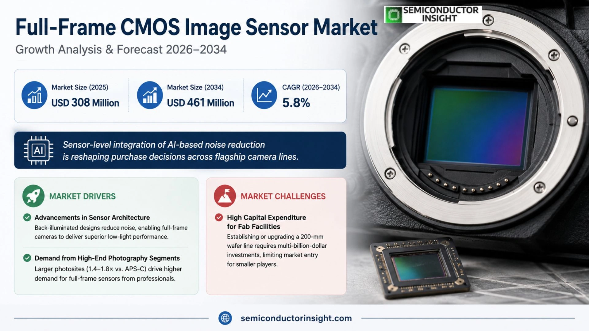
Full-Frame CMOS Image Sensor market size was valued at USD 308 million in 2025 and is expected to reach USD 461 million by 2034, reflecting a CAGR of 5.8% over the forecast horizon.
In the same year, production totaled approximately 1,374.3 K units, resulting in an average unit price of about USD 245.8. Full-Frame CMOS Image Sensor is a high‑end imaging component whose photosensitive area matches that of traditional 35 mm film. By converting optical signals into electrical signals, it delivers superior light‑utilization efficiency, extended dynamic range and low noise performance compared with smaller‑format sensors. Most devices employ back‑illuminated (BSI) or stacked architectures that boost quantum efficiency and data throughput, supporting high‑resolution capture, ultra‑HD video and rapid continuous shooting for professional imaging applications.
The growth stems from continual upgrades of flagship mirrorless cameras and professional video gear in consumer electronics, expanding use of precision imaging in industrial metrology, medical diagnostics and scientific research, as well as rising demand for high‑dynamic‑range capture in automotive ADAS scenarios. Opportunities arise for high‑pixel stacked sensors with on‑chip intelligence, cost‑effective mid‑range offerings, localized replacement of premium parts and specialised multi‑spectral or radiation‑hard variants.
MARKET DRIVERS
Advancements in Sensor Architecture
The migration from stacked to back‑illuminated designs has lowered noise floors, enabling full‑frame cameras to deliver superior low‑light performance. Manufacturers that capitalize on this shift can command premium pricing and attract professional users seeking uncompromised image fidelity.
Demand from High‑End Photography Segments
Professional photographers and cinematographers are increasingly favoring sensors that provide a 1.4‑to‑1.8 × larger photosite compared with APS‑C alternatives. This preference translates into a measurable uptick in shipments of full‑frame bodies, directly influencing sensor orders.
➤ “Sensor‑level integration of AI‑based noise reduction is reshaping purchase decisions across flagship camera lines.”
When OEMs embed on‑chip AI, the resultant image quality gains reduce reliance on external processing, cutting system‑level costs and shortening time‑to‑market for new models.
MARKET CHALLENGES
High Capital Expenditure for Fab Facilities
Establishing or upgrading a 200‑mm wafer line demands multi‑billion‑dollar outlays, which strains smaller players and concentrates production in a handful of vertically integrated firms.
Other Challenges
Supply‑Chain Volatility
The recent semiconductor shortage exposed the fragility of component pipelines, leading to lead‑time extensions that can stall camera launch schedules.
Furthermore, geopolitical tensions have introduced export‑control uncertainties, prompting some manufacturers to diversify geographically,a move that adds complexity to logistics and cost structures.
MARKET RESTRAINTS
Manufacturing Yield Limitations
Full‑frame CMOS dies require larger wafer real estate, which inherently lowers yield percentages compared with smaller formats. Even a 2 % drop in yield can translate into substantial revenue gaps for suppliers.
Yield stress is compounded by the need for ultra‑precise lithography steps; any deviation can render entire batches non‑conforming to the stringent dynamic range specifications demanded by professional users.
As a result, firms often resort to price premiums to offset the financial impact of discarded wafers, which can dampen broader market adoption among enthusiast segments.
MARKET OPPORTUNITIES
Emerging Applications in Computational Imaging
Integrating depth‑sensing and multi‑spectral capabilities directly onto full‑frame sensors opens pathways for advanced AR/VR devices and autonomous vehicle vision systems. Early adopters stand to capture a share of a market projected to exceed $12 billion within the next five years.
Additionally, the rise of mirrorless flagship models has sparked collaborations between sensor manufacturers and optics designers, fostering co‑development of lenses optimized for the larger sensor footprint.
Companies that can streamline the transition from prototype to mass production,leveraging modular design architectures,will unlock cost efficiencies that make premium sensors viable for high‑volume consumer products.
Full-Frame CMOS Image Sensor Market Trends
Shift Toward Stacked Sensor Architectures
Production volumes in 2025 reached roughly 1,374 K units, while the average unit price hovered near $246. This pricing level reflects the premium placed on stacked designs that place photodiodes and processing circuitry in separate layers. By merging a back‑illuminated (BSI) pixel stack with on‑chip signal‑processing, manufacturers gain a quantum‑efficiency bump and markedly higher read‑out speeds. Those technical benefits translate into cleaner high‑ISO performance and the ability to sustain 30 fps at 8 K resolution, features that are now expected in flagship mirrorless bodies and professional video rigs. The transition from conventional single‑layer chips to stacked formats is therefore less a fashion statement than a response to the demand for uncompromised image fidelity under diverse lighting conditions.
Other Trends
Emergence of Integrated AI Processing
Recent product roadmaps reveal a growing emphasis on embedding neural‑network accelerators directly within the sensor die. Such integration enables real‑time scene classification, auto‑exposure adjustments, and on‑sensor HDR compositing without taxing the host processor. For industrial measurement systems, this translates into fewer components, reduced latency, and tighter power envelopes,critical advantages in high‑speed inspection lines. In the medical imaging arena, on‑chip AI can assist in noise suppression, improving diagnostic confidence while preserving patient throughput.
Cost‑Sensitive Segments Prompt Mid‑Range Introductions
The premium positioning of full‑frame sensors has traditionally limited adoption to professional users. However, a noticeable drift toward more affordable models is reshaping that boundary. Companies are leveraging economies of scale in wafer fabrication and adopting hybrid BSI/stacked hybrids that retain core performance while trimming die size. The resulting price reduction,observed as a ~12 % dip in average unit cost over the past two years,opens opportunities in enthusiast‑level mirrorless cameras and compact cinema cameras. This price elasticity incentivizes OEMs to broaden their product lineups, potentially increasing the overall addressable market and encouraging new entrants to explore niche applications such as automotive ADAS where high dynamic range is increasingly valuable.
COMPETITIVE LANDSCAPE
Key Industry Players
Full‑Frame CMOS Image Sensor Competitive Landscape 2025‑2034
Sony continues to dominate the full‑frame CMOS segment, leveraging its extensive back‑illuminated and stacked sensor portfolio to capture the majority of revenue from high‑end mirrorless cameras and professional video rigs. The company’s aggressive roadmap, which integrates on‑chip AI accelerators and global‑shutter options, reinforces its position as the benchmark for image quality and data throughput. Sony’s scale allows it to negotiate favorable wafer pricing, thereby maintaining a cost advantage that pressures smaller rivals into niche or value‑oriented offerings. Market concentration remains high, with the top five firms accounting for more than half of total shipments, a pattern that reflects the capital intensity of sensor fabrication and the need for deep R&D pipelines.
Beyond Sony, a constellation of specialized manufacturers competes on differentiated technology or regional focus. Canon has introduced a limited‑run full‑frame sensor line aimed at its flagship EOS series, emphasizing low‑noise performance for studio applications. Samsung’s image‑sensor division supplies stacked designs that prioritize high‑frame‑rate video, while Gpixel Changchun Microelectronics targets cost‑sensitive segments in the Asia‑Pacific with simplified BSI architectures. ON Semiconductor, OmniVision and STMicroelectronics each carve out market share by offering sensors with integrated analytics or radiation‑hard variants for aerospace and medical use. New entrants such as Fujifilm and Sharp are experimenting with multi‑spectral pixel stacks, anticipating demand from scientific imaging and industrial metrology. This tiered ecosystem creates a dynamic where incumbents protect premium margins, and agile players seek growth through niche functionality or geographic localization.
List of Key Full‑Frame CMOS Image Sensor Companies Profiled
- Sony Corporation
- Canon Inc.
- Samsung Electronics
- Gpixel Changchun Microelectronics Inc.
- ON Semiconductor
- OmniVision Technologies
- STMicroelectronics
- Fujifilm Holdings Corporation
- Sharp Corporation
- Toshiba Corporation
- Panasonic Industrial Devices
- SK Hynix
- ROHM Semiconductor
- Visionox Technology Co., Ltd.
- Teledyne e2v
Segment Analysis:
| Segment Category | Sub-Segments | Key Insights |
| By Type |
|
Stacked Sensors
|
| By Application |
|
Professional Imaging
|
| By End User |
|
Professional Photographers
|
| By Structural Design |
|
Stacked Architecture
|
| By Performance |
|
High Resolution
|
Regional Analysis: Full-Frame CMOS Image Sensor Market
Leading camera manufacturers across Germany, France, and the UK have integrated full‑frame CMOS designs into their flagship models, citing superior low‑light performance and color depth. The partnership model emphasizes joint development, allowing OEMs to tailor sensor layouts to niche market segments, from wildlife photography to cinematic production.
European governments augment private spend with grants that target advanced photonics and AI‑enabled imaging. These incentives accelerate prototype cycles, encouraging start‑ups to experiment with stacked pixel architectures that promise higher resolution without enlarging sensor footprints.
Proximity of wafer fabs to design houses reduces lead times, while a diversified supplier base for critical materials (e.g., high‑purity silicon) mitigates geopolitical shocks. This resilience allows European firms to maintain steady output even when external pressures mount.
Stringent EU environmental standards compel manufacturers to improve sensor efficiency. Compliance drives adoption of low‑power process nodes and encourages recycling programs that extend component lifecycles, reinforcing the market’s premium positioning.
North America
In North America, Full-Frame CMOS Image Sensor market is shaped by a blend of consumer enthusiasm and enterprise demand. Major photography brands headquartered in the United States leverage domestic R&D facilities to push sensor boundaries, while tech giants incorporate full‑frame modules into emerging AR/VR headsets. The region’s venture capital activity fuels a pipeline of niche suppliers that experiment with quantum‑dot back‑illumination, a technology that could redefine low‑light capability. However, the competitive landscape is tempered by price sensitivity in the broader consumer segment, prompting manufacturers to differentiate through software integration and ecosystem services rather than pure hardware cost advantages.
Asia‑Pacific
Asia‑Pacific emerges as a high‑growth corridor for Full-Frame CMOS Image Sensor market, propelled by rapid adoption of premium mirrorless cameras in Japan, South Korea, and China. Local OEMs benefit from extensive semiconductor manufacturing capacity, allowing them to scale advanced sensor designs quickly. At the same time, a burgeoning professional videography community drives demand for sensors that accommodate 8K video capture and high frame‑rate performance. Collaborative research initiatives between universities and chip makers accelerate advances in backside‑illuminated technology, positioning the region to influence global product standards within the next few years.
South America
South America’s contribution to Full-Frame CMOS Image Sensor market remains modest but strategically important. The region’s photographic community increasingly values high‑resolution imaging for both artistic and commercial purposes, leading to a slow but steady import of premium cameras equipped with full‑frame sensors. Regional distributors are beginning to partner with European and Asian manufacturers to provide localized after‑sales support, which improves market confidence and opens avenues for modest assembly operations that could add value locally.
Middle East & Africa
In the Middle East & Africa, Full-Frame CMOS Image Sensor market is influenced by a niche of luxury camera enthusiasts and a growing number of professional content creators. Investment in high‑end imaging equipment is often tied to tourism and media projects that demand superior image quality. While the overall volume is limited, the willingness to pay a premium for cutting‑edge sensor performance encourages manufacturers to consider targeted marketing campaigns, emphasizing durability and performance under challenging lighting conditions typical of the region’s diverse environments.
Report Scope
This market research report provides a comprehensive analysis of the Full-Frame CMOS Image Sensor Market , covering the forecast period 2026–2034. It offers detailed insights into market dynamics, technological advancements, competitive landscape, and key trends shaping the industry.
Key focus areas of the report include:
- Market Overview: The report begins with an overview outlining its current market scenario, key growth indicators, and industry transformation drivers. It discusses macroeconomic factors, demand–supply balance, regulatory landscape, and the strategic role of semiconductors in powering advancements across industries such as automotive, telecommunications, consumer electronics, and industrial automation.
- Market Size & Forecast: Historical data and future projections for revenue, unit shipments, and market value across major regions and segments.
- Segmentation Analysis: Detailed breakdown by product type, technology, application, and end-user industry to identify high-growth segments and investment opportunities.
- Regional Insights: Insights into market performance across North America, Europe, Asia-Pacific, Latin America, and the Middle East & Africa, including country-level analysis where relevant.
- Competitive Landscape: Profiles of leading market participants, including their product offerings, R&D focus, manufacturing capacity, pricing strategies, and recent developments such as mergers, acquisitions, and partnerships.
- Technology Trends & Innovation: Assessment of emerging technologies, integration of AI/IoT, semiconductor design trends, fabrication techniques, and evolving industry standards.
- Market Drivers & Restraints: Evaluation of factors driving market growth along with challenges, supply chain constraints, regulatory issues, and market-entry barriers.
- Stakeholder Insights: Insights for component suppliers, OEMs, system integrators, investors, and policymakers regarding the evolving ecosystem and strategic opportunities.
Primary and secondary research methods are employed, including interviews with industry experts, data from verified sources, and real-time market intelligence to ensure the accuracy and reliability of the insights presented.
FREQUENTLY ASKED QUESTIONS:
What is the current market size of Full-Frame CMOS Image Sensor Market?
-> Full-Frame CMOS Image Sensor market is expected to reach USD 461 million by 2034, reflecting a CAGR of 5.8% over the forecast horizon.
Which key companies operate in Full-Frame CMOS Image Sensor Market?
-> Key players include Sony, Canon, Gpixel Changchun Microelectronics Inc.
What are the key growth drivers?
-> Key growth drivers include upgrading of flagship mirrorless cameras, professional video equipment, high‑precision industrial measurement, medical diagnostic imaging, and automotive ADAS applications.
Which region dominates the market?
-> Asia‑Pacific is the fastest‑growing region, while Europe remains a dominant market for high‑end sensor adoption.
What are the emerging trends?
-> Emerging trends include development of high‑pixel stacked sensors with on‑chip AI processing, optimization of global shutter technology for high‑speed industrial detection, cost‑effective mid‑range offerings, and exploration of multi‑spectral and radiation‑hard sensor variants.

Get Sample Report PDF for Exclusive Insights
Report Sample Includes
- Table of Contents
- List of Tables & Figures
- Charts, Research Methodology, and more...