Key Statistics
Key Takeaways
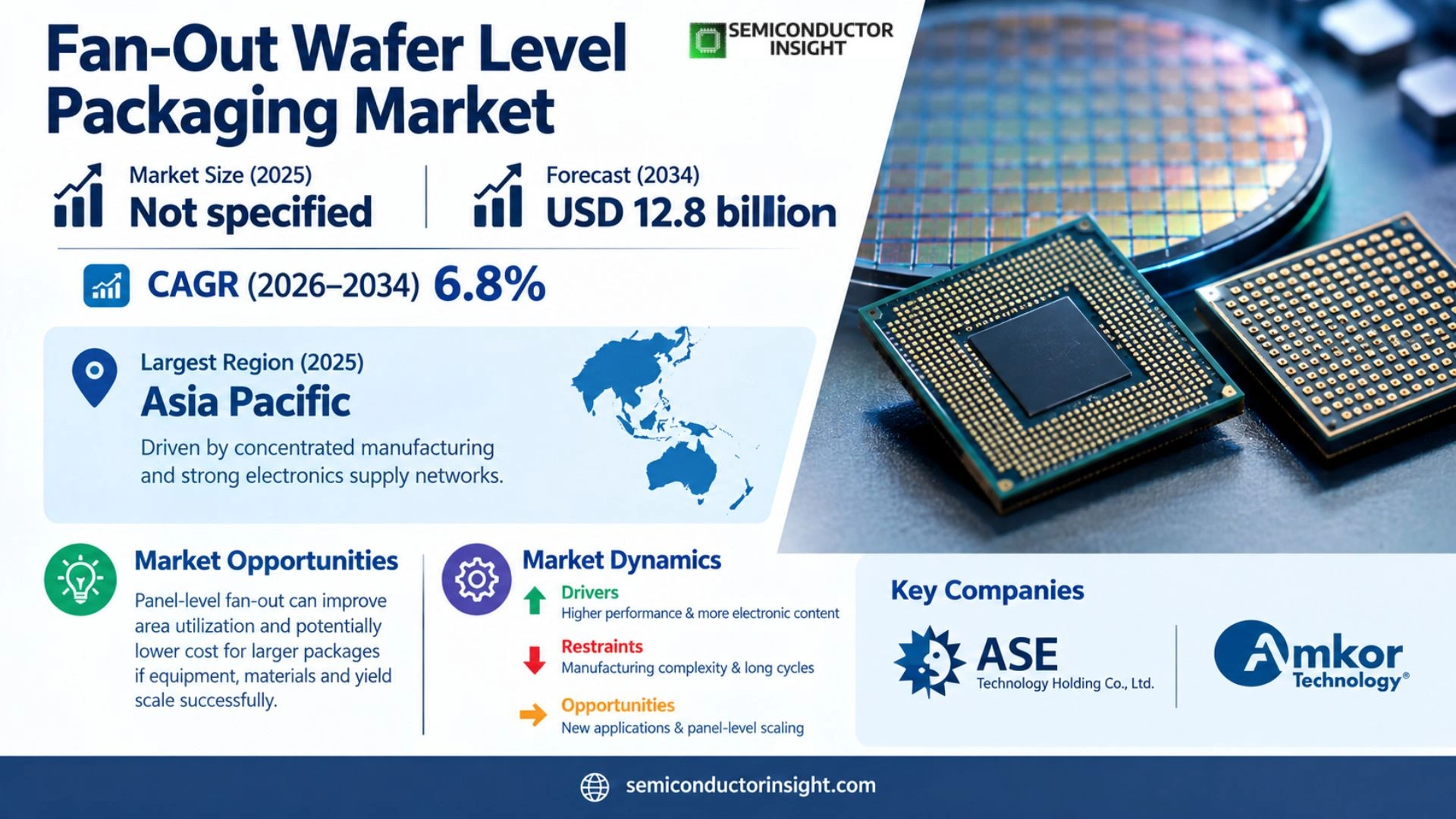
- The Fan-Out Wafer Level Packaging Market was valued at USD 7.1 billion in the 2025 base year and is projected to reach USD 12.8 billion by 2034, expanding at a 6.8% CAGR during 2026–2034.
- FBGA-based fan-out leads by type because it combines thin construction and dense routing with compatibility across established semiconductor package and board-assembly workflows.
- Smartphones remain the largest volume application, while automotive sensing, antenna-in-package, edge AI, and high-performance multi-die systems broaden the technology’s addressable market.
- Asia Pacific dominates through concentrated foundry, outsourced assembly and test, materials, equipment, electronics manufacturing, smartphone, and automotive ecosystems.
- Yield determines capacity economics. Die shift, warpage, redistribution-layer defects, material interactions, known-good-die quality, and final test performance decide cost per qualified package.
Fan-Out Wafer Level Packaging Market Overview
Fan-Out Wafer Level Packaging Market was valued at USD 7.1 billion in 2025 and is projected to reach USD 12.8 billion by 2034, growing at a CAGR of 6.8% during 2026–2034. Asia Pacific held the largest regional position in 2025, supported by concentrated manufacturing, downstream electronics production and established component supply networks.
Fan-out wafer-level packaging builds redistribution layers across a reconstituted wafer or molded carrier so electrical connections can extend beyond the original die footprint. The architecture removes or reduces dependence on a conventional laminate substrate and can support thin profiles, short interconnects, multiple dies, passive integration, and dense input-output routing. Commercial platforms range from low-density single-die packages to high-density system-level structures for mobile, networking, automotive, and computing applications.
The market enters the 2026 estimated year with strong demand from smartphones, connectivity modules, power management, automotive sensors, wearables, and heterogeneous integration. Growth through 2034 will be supported by greater functional density, finer redistribution layers, larger package formats, antenna-in-package adoption, chiplet architectures, and the need to reduce electrical distance between logic, memory, radio-frequency, and analog functions without relying exclusively on costly silicon interposers.
Economics depend on die size, package area, redistribution-layer count and pitch, mold and carrier process, known-good-die quality, warpage, placement accuracy, panel or wafer utilization, and final test yield. Fan-out can deliver compelling electrical and form-factor advantages, but cost leadership is not automatic. Suppliers must align design rules, materials, equipment, simulation, assembly sequence, and customer qualification to achieve stable yield at the intended volume and product mix.
Segment Analysis: By Type
By type, the Fan-Out Wafer Level Packaging market is segmented into FBGA-Based FO-WLP · Chip-on-Wafer FO-WLP. Each category represents a different degree of integration, qualification burden and value capture, so suppliers compete through a combination of material performance, design support, manufacturing consistency, package architecture and application-specific testing rather than through unit price alone. Procurement also reflects lifecycle support, interoperability, compliance evidence, warranty exposure, and the cost of unsuccessful qualification.
| Type | Market relevance |
|---|---|
| FBGA-Based FO-WLP | Distinct performance, condition, integration, and qualification requirements shape demand and supplier positioning. |
| Chip-on-Wafer FO-WLP | Distinct performance, condition, integration, and qualification requirements shape demand and supplier positioning. |
Segment Analysis: By Application
By application, the market covers Smartphones · Wearables · Automotive Sensors · IoT Devices. Demand varies by production volume and qualification intensity: consumer programmes reward scale and miniaturisation, while automotive, industrial, aerospace, medical or security designs place greater weight on reliability evidence, long product availability and system-level performance under demanding operating conditions. Channel design, documentation, service coverage, and total ownership economics further determine which application converts technical interest into repeat purchasing.
| Application | Market relevance |
|---|---|
| Smartphones | Purchasing criteria reflect use-case economics, technical requirements, warranty expectations, and channel support. |
| Wearables | Purchasing criteria reflect use-case economics, technical requirements, warranty expectations, and channel support. |
| Automotive Sensors | Purchasing criteria reflect use-case economics, technical requirements, warranty expectations, and channel support. |
| IoT Devices | Purchasing criteria reflect use-case economics, technical requirements, warranty expectations, and channel support. |
Regional Analysis
Asia Pacific is the largest regional market for Fan-Out Wafer Level Packaging products, combining an established component-production ecosystem with major downstream customers. North America and Europe are strategically important for premium, automotive, aerospace, industrial and specialised applications, while South America and Middle East & Africa are primarily import- and project-led markets where distributor reach, local support and supply continuity shape vendor selection.
How does regional demand differ across this market?
For Fan-Out Wafer Level Packaging, Asia Pacific holds the largest position, supported by an established customer base, supplier presence, and mature purchasing channels. Europe contributes regulation, industrial demand, and technical expertise, while Asia Pacific combines electronics manufacturing, large device populations, and expanding engineering capability. South America and the Middle East and Africa develop through targeted infrastructure, enterprise, research, consumer, or public-sector programs rather than uniform adoption.
| Region | Position |
|---|---|
| Asia Pacific | Largest and most established demand base |
| North America | Developing demand shaped by local applications, channels, and qualification conditions |
| Europe | Developing demand shaped by local applications, channels, and qualification conditions |
| South America | Developing demand shaped by local applications, channels, and qualification conditions |
| Middle East & Africa | Developing demand shaped by local applications, channels, and qualification conditions |
Key Fan-Out Wafer Level Packaging Manufacturers and Competitive Landscape
The Fan-Out Wafer Level Packaging competitive landscape includes global technology leaders, diversified semiconductor or component groups, RF and imaging specialists, and regional manufacturers. The report profiles every named company across product positioning, manufacturing footprint, application exposure, recent development activity and strategic strengths; the complete coverage list is reproduced below so the intended company universe is explicit.
The report covers ASE Technology Holding, Amkor Technology, TSMC, JCET Group, STATS ChipPAC, Nepes, Powertech Technology, Siliconware Precision Industries, Unimicron Technology, Deca Technologies, Infineon Technologies, STMicroelectronics, Huatian Technology, Tongfu Microelectronics, and Jiangsu Changjiang Electronics Technology. Competition spans foundry-integrated packaging, global outsourced assembly and test groups, regional packaging specialists, substrate companies, technology licensors, and integrated device manufacturers.
Vendors differentiate through redistribution-layer density, package size, die count, placement accuracy, warpage control, thermal design, electrical performance, embedded passives, antenna integration, design enablement, production yield, and qualification history. Scale and customer proximity are important because programs require close co-development between chip, package, and system teams. Proprietary design rules and process flows can create switching costs, while licensed technologies and common tool support can broaden adoption across multiple manufacturing partners.
Key companies profiled
- ASE Technology Holding Co., Ltd.
- Amkor Technology, Inc.
- Taiwan Semiconductor Manufacturing Company (TSMC)
- JCET Group Co., Ltd.
- STATS ChipPAC Pte. Ltd.
- Nepes Corporation
- Powertech Technology Inc.
- Siliconware Precision Industries Co., Ltd.
- Unimicron Technology Corporation
- Deca Technologies Inc.
- Infineon Technologies AG
- STMicroelectronics N.V.
- Huatian Technology Co., Ltd.
- Tongfu Microelectronics Co., Ltd.
- Jiangsu Changjiang Electronics Technology Co., Ltd.
Fan-Out Wafer Level Packaging Production Capacity Analysis
Production capacity is a material competitive factor in the Fan-Out Wafer Level Packaging market because electrical performance depends on specialised processes, qualified materials, repeatable yields and application-specific test capability. Capacity cannot be assessed only by nominal factory floor area: effective supply is the output that passes dimensional, electrical, reliability and customer qualification requirements at the required product mix.
Effective capacity is measured by qualified reconstituted-wafer or panel output at acceptable yield, not by nominal cleanroom area. Production requires die preparation, known-good-die selection, high-accuracy placement, temporary carriers, molding, grinding, redistribution-layer lithography, copper plating, dielectric processing, bumping, singulation, test, and inspection. Bottlenecks can occur in placement, exposure field size, warpage handling, multilayer RDL yield, or final electrical test even when molding capacity is available.
High-density fan-out increases process sensitivity. Die shift during molding must be corrected by adaptive alignment or design compensation; large packages amplify warpage and carrier-release risk; fine lines and spaces demand advanced lithography, clean surfaces, uniform plating, and defect inspection. Capacity expansion therefore includes metrology, modeling, automated material handling, and process control. A supplier that adds equipment without stabilizing these interactions may increase starts while producing little additional customer-qualified output.
Product mix affects utilization because mobile packages, automotive sensors, antenna modules, and multi-die computing structures use different wafer formats, RDL layers, materials, test flows, and qualification standards. High-volume consumer programs reward throughput and cost, whereas automotive and HPC packages require more complex reliability and thermal verification. Modular process platforms, shared design kits, and flexible lines allow manufacturers to allocate capacity across applications without creating excessive changeover loss or fragmented engineering support.
Fan-Out Wafer Level Packaging Market Dynamics: Drivers, Restraints and Opportunities
Fan-Out Wafer Level Packaging market growth reflects expanding electronic content and higher performance requirements, moderated by manufacturing complexity, long qualification cycles and competing technologies. The impact ranges below are directional analytical estimates rather than additive forecasts; they show the relative pressure each factor can place on the baseline CAGR when other assumptions remain broadly stable.
Growth reflects the semiconductor industry’s shift from transistor scaling alone toward system-level performance through advanced packaging. Fan-out reduces interconnect length, enables thinner products, and supports heterogeneous integration across logic, memory, RF, analog, sensors, and passives. Demand can be concentrated because a small number of high-volume mobile or computing designs materially affect factory loading. Qualification timing and customer product cycles therefore create pronounced differences between technology adoption and annual revenue recognition.
The market competes with flip-chip ball-grid arrays, wafer-level chip-scale packages, embedded-die substrates, 2.5D interposers, and other chiplet platforms. Fan-out wins when electrical performance, package thickness, integration density, and total cost align with the application. It can lose when die size, package area, yield risk, thermal requirements, or substrate availability favors another architecture. Suppliers must offer credible design comparison and manufacturing evidence rather than positioning fan-out as universally superior.
MARKET DRIVERS
Drivers Impact Analysis*
| Driver | (~) % impact on CAGR forecast | Geographic relevance | Impact timeline |
|---|---|---|---|
| Mobile and wearable miniaturization | +1.5% | Asia Pacific and global device brands | Short term (≤2 years) |
| AI and high-performance multi-die integration | +1.2% | Taiwan, United States, South Korea | Long term (≥4 years) |
| 5G/6G antenna-in-package adoption | +0.9% | Asia Pacific, North America, Europe | Medium term (2–4 years) |
| Automotive radar, sensing and connectivity | +0.8% | China, Europe, Japan, North America | Long term (≥4 years) |
| Panel-level fan-out development | +0.6% | Taiwan, South Korea, China, Europe | Medium term (2–4 years) |
| Design kits and adaptive patterning | +0.4% | Global packaging design ecosystem | Short term (≤2 years) |
Mobile and wearable devices drive volume because designers require thin packages, dense routing, lower parasitics, and integration of application processors, power management, radio-frequency components, sensors, and passives in restricted space. Fan-out supports compact system-in-package and package-on-package configurations while avoiding some conventional substrate constraints. Continued demand depends on cost per good package, device roadmap alignment, antenna performance, thermal management, and the ability to deliver large consumer ramps without yield volatility.
Artificial intelligence and high-performance computing are expanding the addressable market toward larger, denser fan-out structures. Chiplet systems need short, high-bandwidth links between compute, I/O, memory, and specialized accelerators. Fan-out bridges and high-density RDL can complement organic substrates or provide alternatives for selected architectures. Growth requires control of large-package warpage, power delivery, thermal paths, signal integrity, repair strategy, and known-good-die risk across expensive multi-die assemblies.
Automotive electronics create a qualification-led demand stream for radar, connectivity, power management, sensors, and advanced driver-assistance modules. Fan-out can reduce size and improve high-frequency performance, but vehicle programs require temperature cycling, moisture resistance, mechanical robustness, traceability, and long availability. Suppliers that establish automotive-grade process controls and regional support can convert technical advantages into durable programs, although design cycles are slower and change management is stricter than in consumer electronics.
MARKET RESTRAINTS
Restraints Impact Analysis*
| Restraint | (~) % impact on CAGR forecast | Geographic relevance | Impact timeline |
|---|---|---|---|
| Complex process integration and capital intensity | −1.3% | All advanced-packaging regions | Persistent |
| Warpage, die shift and multilayer RDL yield | −1.0% | Large and high-density packages | Persistent |
| Alternative advanced-packaging architectures | −0.7% | Mobile, computing and automotive | Medium term (2–4 years) |
| Known-good-die and multi-die assembly risk | −0.5% | AI, HPC and heterogeneous systems | Long term (≥4 years) |
| Specialized materials and engineering talent | −0.4% | Emerging production locations | Medium term (2–4 years) |
Process complexity and capital intensity restrain adoption. Reconstitution, molding, carrier handling, fine-line lithography, plating, dielectric formation, inspection, and test require specialized equipment and integration expertise. Multilayer RDL and large packages increase defect opportunities, while design changes can require new masks and validation. Smaller providers may struggle to fund capacity before customer commitment, but customers may hesitate to commit until the supplier demonstrates stable yield, creating a difficult scale-up sequence.
Warpage, die shift, and material interactions can reduce yield. Mold compound shrinkage, carrier behavior, dielectric stress, copper density, package geometry, and thermal history interact across the process. Placement errors can misalign redistribution layers, while excessive warpage affects lithography, handling, assembly, and board-level reliability. Modeling and adaptive patterning help, but each package requires design-specific verification, making rapid transfer between sites or material sets more difficult than nominal process descriptions suggest.
Alternative packaging architectures limit market penetration. Flip-chip substrates provide mature infrastructure for many processors, wafer-level chip-scale packages remain economical for small dies, and silicon interposers or hybrid-bonded structures offer extreme density for premium computing. Customers compare total package cost, yield, thermal performance, test access, supply capacity, and roadmap risk. Fan-out suppliers must show application-specific advantages and avoid excessive proprietary lock-in that discourages second sourcing or long-term platform adoption.
MARKET OPPORTUNITIES
Panel-level fan-out can improve area utilization and potentially lower cost for larger packages if equipment, materials, and yield scale successfully. Rectangular panels offer more usable area than round wafers, but larger formats increase challenges in warpage, uniformity, lithography, handling, and standards. Suppliers that develop stable panel processes, interoperable materials, and scalable inspection can address chiplets, power devices, automotive modules, and other applications needing more package area than traditional mobile fan-out.
Antenna-in-package creates opportunities in 5G, future 6G, radar, satellite, and short-range sensing. Fan-out can integrate RF dies, antennas, passives, and redistribution structures with short electrical paths and compact form factors. Performance depends on low-loss materials, dimensional accuracy, electromagnetic design, shielding, thermal behavior, and test strategy. Collaboration among RF chip vendors, packaging houses, materials suppliers, and system OEMs is essential because package geometry directly affects antenna and radio performance.
Design enablement and technology licensing can expand adoption beyond factories owned by a single provider. Package assembly design kits, simulation models, automated routing, adaptive patterning, and verified reference flows reduce iteration between die and packaging teams. Licensing can create multi-source capacity for successful architectures while generating royalty and engineering revenue. The strongest opportunities combine differentiated process intellectual property with tools that make yield, reliability, and electrical behavior predictable before physical qualification begins.
Fan-Out Wafer Level Packaging Supply Chain Analysis
The Fan-Out Wafer Level Packaging supply chain links specialty materials and wafer or ceramic processing equipment to high-precision manufacturing, packaging, distribution and downstream system integration. Commercial resilience depends on qualified alternate materials, realistic yield assumptions, geographic redundancy and traceable process controls because a nominal second source is not interchangeable until the customer has validated electrical behaviour, reliability and package compatibility.
The supply chain begins with known-good semiconductor dies, redistribution-layer metals, dielectric polymers, mold compounds, carriers, release materials, photoresists, plating chemicals, under-bump materials, balls, and test interfaces. Equipment suppliers provide placement, molding, grinding, lithography, plating, inspection, and singulation systems. Foundries, outsourced assembly and test companies, design-tool vendors, substrate partners, and OEMs coordinate architecture, simulation, manufacturing, final test, board assembly, and system qualification.
Resilience depends on material qualification, equipment matching, and customer-approved site transfer. Changing mold compound, dielectric, carrier, plating chemistry, exposure tool, or placement platform can alter warpage, adhesion, line geometry, moisture behavior, and reliability. Strong programs maintain detailed process windows, lot traceability, statistical data, approved alternates, spare tooling, and shared failure analysis. Geographic redundancy becomes useful only after the second line reproduces design rules, yield, and reliability for the customer’s exact package.
Recent Developments in the Fan-Out Wafer Level Packaging Market
Developments tracked to September 2026 and linked to official company or industry sources.
- October 2025 Published
ASE published an analysis of fan-out panel-level packaging opportunities and challenges for AI and high-performance computing, emphasizing larger package formats, process control, and heterogeneous integration requirements. Source - June 2025 Published
ASE presented research on a 300-millimeter panel-level fan-out approach designed for chiplet integration in high-performance computing, including advanced redistribution and large-format process development. Source - May 2025 Published
ASE announced FOCoS-Bridge with through-silicon vias as an advanced fan-out structure designed to reduce power loss and support high-bandwidth AI and computing packages. Source - December 2025 Published
ASE detailed VIPack as a scalable advanced-packaging platform that includes high-density redistribution-layer fan-out package-on-package and fan-out chip-on-substrate technologies for heterogeneous integration. Source - February 2025 Published
Amkor’s annual filing described wafer-level fan-out packages for power management, transceivers, radar, specialty silicon, and multi-die applications, confirming continued commercial deployment across diverse end markets. Source
REPORT SCOPE & SEGMENTATION
| Attribute | Details |
|---|---|
| Study Period | 2021–2034 |
| Base Year | 2025 |
| Estimated Year | 2026 |
| Forecast Year | 2034 |
| Historical Period | 2021–2025 |
| Market Size 2025 | USD 7.1 billion |
| Market Size 2034 | USD 12.8 billion |
| Growth Rate | CAGR of 6.8% from 2026–2034 |
| Unit | Value in USD billion and shipment or production volume where disclosed |
| Segmentation | By Type, By Application, additional technology axis and By Region |
| By Type | FBGA-Based FO-WLP · Chip-on-Wafer FO-WLP |
| By Application | Smartphones · Wearables · Automotive Sensors · IoT Devices |
| By Integration Approach and Device Category | Heterogeneous Integration · System-in-Package · Antenna-in-Package · Mobile Communications · Advanced Driver-Assistance Systems · Medical Wearables |
| By Region | Each region analysed by type, application and countryNorth AmericaU.S., Canada, MexicoEuropeGermany, France, U.K., Italy, Nordic Countries, BeneluxAsia PacificChina, Japan, South Korea, India, Southeast AsiaSouth AmericaBrazil, Argentina, Rest of South AmericaMiddle East & AfricaTurkey, Israel, Saudi Arabia, UAE, Rest of MEA |
| Key Companies Profiled | ASE Technology Holding Co., Ltd.; Amkor Technology, Inc.; Taiwan Semiconductor Manufacturing Company (TSMC); JCET Group Co., Ltd.; STATS ChipPAC Pte. Ltd.; Nepes Corporation; Powertech Technology Inc.; Siliconware Precision Industries Co., Ltd.; Unimicron Technology Corporation; Deca Technologies Inc.; Infineon Technologies AG; STMicroelectronics N.V.; Huatian Technology Co., Ltd.; Tongfu Microelectronics Co., Ltd.; Jiangsu Changjiang Electronics Technology Co., Ltd. |
| Customization Scope | Free report customization equivalent to up to four analyst working days with purchase, including additions or alterations to country, regional and segment coverage. |
Frequently Asked Questions
What is fan-out wafer-level packaging?
The Fan-Out Wafer Level Packaging Market is valued at USD 7.1 billion in the 2025 base year and is projected to reach USD 12.8 billion by 2034, expanding at a CAGR of 6.8% during 2026–2034. The outlook covers FBGA-based and chip-on-wafer fan-out solutions used across smartphones, wearables, automotive sensors, IoT devices, communications, and heterogeneous systems, with Asia Pacific holding the leading regional position.
What is the market outlook through 2034?
Demand is expected to expand through 2034 as semiconductor companies use advanced packaging to achieve greater functional density, shorter electrical paths, thinner products, and heterogeneous integration. Mobile devices will continue to support volume, while artificial-intelligence hardware, chiplets, antenna-in-package designs, automotive sensors, and edge systems create new value. Suppliers that control warpage, die placement, high-density redistribution layers, thermal behavior, and qualified yield will secure the strongest programs.
Which product type leads?
FBGA-based fan-out holds the leading position because it aligns with established board-assembly practices while providing thinner construction, dense routing, and useful thermal and electrical performance. Chip-on-wafer and higher-density fan-out approaches are gaining importance for multi-die and heterogeneous systems. The appropriate architecture depends on package size, input-output count, redistribution-layer density, test strategy, thermal load, substrate interaction, and target manufacturing cost.
Which applications create the strongest demand?
Smartphones remain the principal volume application because advanced devices require compact application processors, power management, RF functions, connectivity modules, and package-on-package integration. Wearables and IoT devices also value thin form factors and low parasitics. Automotive sensors, radar, and control modules provide qualification-led growth, while artificial-intelligence and high-performance computing create opportunities for larger multi-die fan-out and bridge structures.
Why does Asia Pacific lead?
Asia Pacific concentrates semiconductor foundries, outsourced assembly and test providers, advanced substrates, packaging materials, electronics manufacturing, smartphones, automotive electronics, and major customers across Taiwan, South Korea, China, Japan, and Southeast Asia. TSMC, ASE, JCET, SPIL, Powertech, Nepes, Huatian, and Tongfu strengthen regional capacity. North America remains important for chip design, equipment, materials, technology licensing, and high-performance computing demand.
What drives market growth?
Growth is driven by thinner electronics, higher input-output density, improved signal integrity, heterogeneous integration, chiplet adoption, 5G and future 6G radio modules, automotive electronics, and demand for energy-efficient computing. Fan-out enables redistribution beyond the die and can integrate several functions without a conventional substrate. Continued adoption depends on stable yield, competitive cost, scalable package size, design tools, thermal solutions, and qualified production capacity.
What are the main restraints?
Capital intensity, complex process integration, warpage, die shift, fine-line redistribution-layer defects, material interactions, known-good-die risk, and limited engineering talent restrain adoption. Large or multilayer packages magnify yield and handling challenges. Fan-out also competes with flip-chip substrates, wafer-level chip-scale packaging, embedded-die structures, silicon interposers, and hybrid bonding, requiring suppliers to demonstrate a clear application-specific performance and cost advantage.
How do suppliers compete?
Suppliers compete through redistribution-layer pitch and count, package size, die placement, warpage control, mold and dielectric systems, thermal performance, signal integrity, antenna capability, embedded passives, design enablement, production yield, capacity, and customer qualification. Foundry-integrated providers offer close process coordination, while outsourced assembly and test companies provide broad customer access and manufacturing scale. Technology licensing and adaptive patterning can support differentiated multi-source production strategies.
Where are the best opportunities?
Opportunities include panel-level fan-out, large chiplet packages, fan-out bridges, antenna-in-package, automotive radar and sensors, power management, medical wearables, edge computing, and multi-die system-in-package designs. Design kits, simulation models, adaptive patterning, automated inspection, and licensed process platforms can shorten qualification. Suppliers that solve large-format warpage, thermal management, power delivery, high-density routing, and predictable cost can capture premium computing and communications programs.
Which companies are covered?
The report covers ASE Technology Holding, Amkor Technology, TSMC, JCET Group, STATS ChipPAC, Nepes, Powertech Technology, Siliconware Precision Industries, Unimicron Technology, Deca Technologies, Infineon Technologies, STMicroelectronics, Huatian Technology, Tongfu Microelectronics, and Jiangsu Changjiang Electronics Technology. Profiles examine package platforms, process capability, capacity, applications, geographic reach, technology partnerships, customer positioning, and recent developments for every company included in the report.

Get Sample Report PDF for Exclusive Insights
Report Sample Includes
- Table of Contents
- List of Tables & Figures
- Charts, Research Methodology, and more...
 Download Sample Report PDF