Electroforming Printing Stencil Market Insights
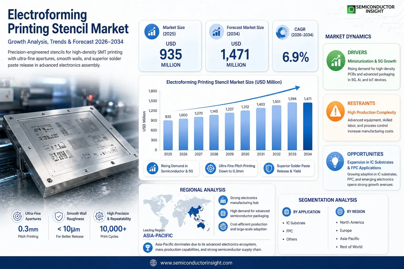
Global Electroforming Printing Stencil market size was valued at USD 935 million in 2025. The market is projected to reach USD 1,471 million by 2034, exhibiting a CAGR of 6.9% during the forecast period.
Electroforming printing stencils are precision-engineered tools essential for high-density printing in electronics assembly. Designed for applications like 0.3mm pitch components and 0.603mm apertures, these stencils feature exceptionally smooth wall roughness. This enhances solder paste release and flow properties, ensuring superior deposit quality in surface mount technology processes.
The market benefits from surging demand in semiconductor packaging and flexible electronics, driven by miniaturization trends and 5G deployment. Furthermore, advancements in IC substrates and FPC manufacturing bolster expansion. Key players such as StenTech, Bon-Mark, BlueRing Stencils, MOKO Technology, Alpha Assembly Solutions, ASMPT SMT Solutions, and Stencils Unlimited dominate with innovative portfolios. Their focus on framed and frameless variants supports diverse applications including IC substrates, FPC, and others.
MARKET DRIVERS
Advancements in Electronics Manufacturing
Electroforming Printing Stencil Market is propelled by the surging demand for high-precision stencils in surface-mount technology (SMT) assembly lines. Electroforming techniques deliver ultra-fine apertures essential for depositing minute amounts of solder paste on increasingly dense PCB layouts, supporting the miniaturization trend in consumer electronics and automotive sectors.
Growth in 5G and Automotive Applications
Expansion of 5G infrastructure and electric vehicle production has intensified the need for reliable stencil solutions. With global PCB production expected to rise by 6.5% annually through 2028, electroformed stencils offer superior durability and repeatability, reducing defects in high-volume manufacturing environments.
➤ Electroforming stencils achieve wall thicknesses below 10 microns, enabling fine-pitch printing down to 0.3mm, which laser alternatives struggle to match consistently.
Additionally, rising investments in semiconductor fabrication further bolster market momentum, as these stencils ensure precise material deposition critical for yield optimization.
MARKET CHALLENGES
Technical Complexity in Production
Producing electroformed printing stencils demands specialized equipment and skilled labor, complicating scalability for smaller manufacturers in Electroforming Printing Stencil Market. Process variations like bath chemistry control can lead to inconsistencies, impacting stencil performance in demanding applications.
Other Challenges
Cost Pressures and Supply Chain Disruptions
High material costs for nickel and precious metal catalysts, coupled with global supply chain volatility, elevate production expenses by up to 15% in recent years, challenging profitability amid competitive pricing demands from electronics OEMs.Competition from alternative technologies, such as laser-cut or etched stencils, adds pressure, as they offer quicker turnaround times despite inferior precision for ultra-fine pitches.
MARKET RESTRAINTS
High Initial Investment Barriers
Electroforming Printing Stencil Market faces significant restraints from substantial capital requirements for cleanroom facilities and proprietary electroforming systems, deterring entry for mid-tier players and limiting market expansion in emerging economies.Environmental regulations on chemical waste disposal from electroforming processes impose additional compliance costs, estimated at 10-12% of operational budgets, slowing adoption in regions with stringent norms like the EU.Dependency on skilled technicians for process optimization remains a bottleneck, as workforce shortages in precision manufacturing hinder consistent output quality and innovation pace.
MARKET OPPORTUNITIES
Innovation in Hybrid Stencil Technologies
Opportunities abound in Electroforming Printing Stencil Market through hybridization with additive manufacturing, enabling custom stencils for advanced packaging like fan-out wafer-level formats, projected to grow at 8% CAGR by 2030.Expansion into medical device assembly and aerospace sectors presents untapped potential, where electroformed stencils’ precision supports micro-scale soldering needs in high-reliability environments.Sustainable electroforming processes using recyclable electrolytes could capture eco-conscious markets, aligning with global green manufacturing initiatives and fostering long-term demand growth.
Electroforming Printing Stencil Market Trends
Rising Adoption in High-Density Electronics Printing
Electroforming Printing Stencil Market is experiencing notable growth driven by the demand for precision in high-density printing applications, such as 0.3mm pitch components and 0.603mm apertures. These stencils feature exceptionally smooth aperture walls that enhance solder paste release properties, enabling reliable performance in advanced PCB assembly processes. Manufacturers are increasingly turning to electroforming technology to meet the challenges of miniaturization in electronics, where traditional stenciling methods fall short in achieving uniform solder deposits. This trend is particularly evident in sectors requiring fine-pitch printing, supporting the production of compact devices with higher component densities.
Other Trends
Shift Towards Framed Stencils
In Electroforming Printing Stencil Market, the framed segment is gaining prominence due to its superior stability and ease of handling in high-volume production environments. Framed stencils provide enhanced tension control and repeatability, making them ideal for automated surface mount technology lines. This preference is influencing supplier strategies, with key players like StenTech, Bon-Mark, and BlueRing Stencils optimizing their portfolios to cater to framed designs. Meanwhile, frameless options continue to serve niche applications where flexibility is prioritized over rigidity.
Expansion in Key Applications and Regions
Electroforming Printing Stencil Market is seeing accelerated uptake in applications like IC substrates and flexible printed circuits (FPC), where precision stenciling is critical for yield optimization. Industry surveys highlight growing demand from these segments, alongside others in advanced packaging. Regionally, Asia, particularly China, Japan, and South Korea, leads with robust manufacturing bases, followed by North America and Europe. Companies such as MOKO Technology, ASMPT SMT Solutions, and Christian Koenen GmbH are responding to these dynamics through product innovations and expanded capacities. Challenges like supply chain obstacles and technical hurdles in aperture refinement persist, yet drivers including industry consolidation and technological advancements foster a positive outlook for sustained market evolution.
COMPETITIVE LANDSCAPE
Key Industry Players
Electroforming Printing Stencil Market Leaders and Dynamics
Electroforming Printing Stencil Market features a competitive landscape led by specialized manufacturers focusing on high-density printing solutions for fine-pitch components such as 0.3mm and 0.603mm apertures. Key leaders including StenTech, Bon-Mark, and BlueRing Stencils command substantial market shares, with the global top five players collectively holding a significant portion of revenue in 2025. This oligopolistic structure is driven by technological barriers in electroforming processes that ensure smooth aperture walls for optimal solder paste release. Companies prioritize innovation in framed and frameless stencils tailored for applications in IC substrates and flexible printed circuits (FPC), amid growing demand from electronics assembly sectors. The market’s moderate concentration fosters strategic partnerships and R&D investments to address challenges like regional supply chain variations across North America, Europe, and Asia.
Beyond the frontrunners, a robust ecosystem of niche players contributes to market diversity, including MOKO Technology, ASMPT SMT Solutions, and MkFF Laserteknique International, which excel in customized solutions for high-precision SMT processes. Firms like Christian Koenen GmbH and Process Lab Micron emphasize European quality standards, while Asian specialists such as Jiangsu Leader Electronic Information Technology and Nantong Zhuolida Metal Technology leverage cost efficiencies and rapid scaling. These secondary competitors target underserved segments like ‘Others’ applications, navigating obstacles such as price fluctuations and raw material dependencies. Overall, the competitive intensity is heightened by mergers, acquisitions, and expansions, positioning the industry for a projected CAGR of 6.9% through 2034, with players differentiating via superior aperture precision and yield improvements in advanced packaging.
List of Key Electroforming Printing Stencil Companies Profiled
- StenTech
- Bon-Mark
- BlueRing Stencils
- MOKO Technology
- Alpha Assembly Solutions
- ASMPT SMT Solutions
- MkFF Laserteknique International
- Stencils Unlimited
- TechnoTronix
- Epec Engineered Technologies
- Christian Koenen GmbH
- Process Lab Micron
- Precision Tech
- MICROEF
- Jiangsu Leader Electronic Information Technology
- Konwin
- Nantong Zhuolida Metal Technology
Segment Analysis:
| Segment Category | Sub-Segments | Key Insights |
| By Type |
|
Framed
|
| By Application |
|
IC Substrate
|
| By End User |
|
Semiconductor Packaging Houses
|
| By Pitch |
|
0.3mm Pitch
|
| By Frame Material |
|
Stainless Steel
|
Regional Analysis: Electroforming Printing Stencil Market
Asia-Pacific
Asia-Pacific’s Electroforming Printing Stencil Market benefits from dense manufacturing hubs, where electroforming excels in producing ultra-thin, high-precision stencils for fine-pitch soldering. Cost-effective raw materials and skilled labor enable rapid prototyping and mass production, catering to smartphone and LED assembly lines.
Regional R&D focuses on hybrid electroforming techniques, improving stencil thickness uniformity and release properties. This supports advanced SMT demands, reducing bridging issues and enhancing yield rates in high-volume electronics fabrication.
Seamless integration with PCB and solder paste suppliers streamlines Electroforming Printing Stencil workflows. Local ecosystems minimize lead times, fostering agile responses to fluctuating demands in consumer and industrial electronics sectors.
Strong export capabilities position Asia-Pacific stencils in global markets, leveraging quality certifications and customization for automotive and telecom applications. Strategic partnerships drive market penetration and technology transfers.
North America
North America’s Electroforming Printing Stencil Market emphasizes innovation and high-reliability applications, particularly in aerospace, defense, and medical devices. Precision engineering firms leverage electroforming for stencils with exceptional edge definition, supporting complex multilayer PCBs. Collaborative ecosystems involving universities and tech giants advance laser-assisted electroforming, enhancing resolution for miniaturized components. Business strategies focus on customization and quick-turn services, catering to prototyping needs. Sustainability initiatives promote recyclable nickel processes, aligning with regulatory pressures. The region’s mature infrastructure facilitates seamless adoption in high-margin sectors, where stencil performance directly impacts assembly yields. Investments in automation refine electroforming consistency, positioning North America as a hub for premium Electroforming Printing Stencil solutions amid evolving electronics demands.
Europe
Europe’s Electroforming Printing Stencil Market is characterized by stringent quality standards and automotive sector integration. Countries like Germany and the UK lead in developing durable electroforming stencils for electric vehicle power electronics and industrial automation. Emphasis on environmental compliance drives adoption of low-emission electroforming baths, ensuring compliance with REACH regulations. Collaborative industry consortia optimize stencil designs for lead-free soldering, reducing voids in high-reliability assemblies. Business strategies prioritize modular production lines, enabling scalability for diverse applications in renewable energy and telecommunications. Precision tolerances achieved through electroforming support Europe’s push towards Industry 4.0, where smart factories demand flawless stencil performance. This fosters a competitive landscape centered on value-added services and long-term partnerships.
South America
South America’s Electroforming Printing Stencil Market is emerging, propelled by growing electronics assembly in Brazil and Mexico. Local manufacturers adopt electroforming to meet demands from consumer goods and renewable energy sectors, focusing on cost-effective stencil production for mid-range PCBs. Investments in training programs enhance technical expertise, bridging skill gaps for finer pitch capabilities. Business strategies emphasize import substitution, with regional firms partnering for technology transfers to build domestic capacity. Infrastructure developments support expanded SMT lines, increasing reliance on reliable electroforming stencils. Challenges like supply volatility are addressed through diversified sourcing, positioning South America for gradual integration into the global Electroforming Printing Stencil ecosystem.
Middle East & Africa
The Middle East & Africa region in Electroforming Printing Stencil Market sees potential growth tied to oil-to-tech diversification and smart city projects. Electroforming stencils gain traction in solar inverters and data center hardware, where precision is critical. Gulf nations invest in high-tech parks, fostering local production of advanced stencils via electroforming for harsh-environment electronics. Africa’s burgeoning telecom infrastructure drives demand for robust stencil solutions. Business strategies involve joint ventures with Asian suppliers, transferring knowledge for customized applications. Emphasis on resilient supply chains supports expansion, with electroforming enabling high-yield printing in resource-constrained settings. Strategic focus on workforce upskilling accelerates adoption across the Electroforming Printing Stencil value chain.
Report Scope
This market research report provides a comprehensive analysis of Electroforming Printing Stencil Market, covering the forecast period 2026–2034. It offers detailed insights into market dynamics, technological advancements, competitive landscape, and key trends shaping the industry.
Key focus areas of the report include:
- Market Overview: The report begins with an overview outlining its current market scenario, key growth indicators, and industry transformation drivers. It discusses macroeconomic factors, demand–supply balance, regulatory landscape, and the strategic role of electroforming printing stencils in powering advancements across industries such as automotive, telecommunications, consumer electronics, and industrial automation.
- Market Size & Forecast: Historical data and future projections for revenue, unit shipments, and market value across major regions and segments.
- Segmentation Analysis: Detailed breakdown by product type, technology, application, and end-user industry to identify high-growth segments and investment opportunities.
- Regional Insights: Insights into market performance across North America, Europe, Asia-Pacific, Latin America, and the Middle East & Africa, including country-level analysis where relevant.
- Competitive Landscape: Profiles of leading market participants, including their product offerings, R&D focus, manufacturing capacity, pricing strategies, and recent developments such as mergers, acquisitions, and partnerships.
- Technology Trends & Innovation: Assessment of emerging technologies, integration of AI/IoT, semiconductor design trends, fabrication techniques, and evolving industry standards.
- Market Drivers & Restraints: Evaluation of factors driving market growth along with challenges, supply chain constraints, regulatory issues, and market-entry barriers.
- Stakeholder Insights: Insights for component suppliers, OEMs, system integrators, investors, and policymakers regarding the evolving ecosystem and strategic opportunities.
Primary and secondary research methods are employed, including interviews with industry experts, data from verified sources, and real-time market intelligence to ensure the accuracy and reliability of the insights presented.
FREQUENTLY ASKED QUESTIONS:
What is the current market size of Electroforming Printing Stencil Market?
-> Electroforming Printing Stencil Market was valued at USD 935 million in 2025 and is expected to reach USD 1471 million by 2034, growing at a CAGR of 6.9% during the forecast period.
Which key companies operate in Electroforming Printing Stencil Market?
-> Key players include StenTech, Bon-Mark, BlueRing Stencils, MOKO Technology, Alpha Assembly Solutions, ASMPT SMT Solutions, MkFF Laserteknique International, Stencils Unlimited, TechnoTronix, Epec Engineered Technologies, among others.
What are the key growth drivers?
-> Key growth drivers include demand for high-density printing stencils supporting 0.3mm pitch and 0.603mm components, smooth aperture walls for improved solder paste release, and expansion in IC substrate and FPC applications.
Which region dominates the market?
-> Asia is the fastest-growing region, while North America remains a key market.
What are the emerging trends?
-> Emerging trends include advancements in electroforming for ultra-fine pitch stencils, focus on Framed and Frameless types, and growth in applications for IC Substrate, FPC, and others.

Get Sample Report PDF for Exclusive Insights
Report Sample Includes
- Table of Contents
- List of Tables & Figures
- Charts, Research Methodology, and more...