Compound Semiconductor Inspection Equipment Market Insights
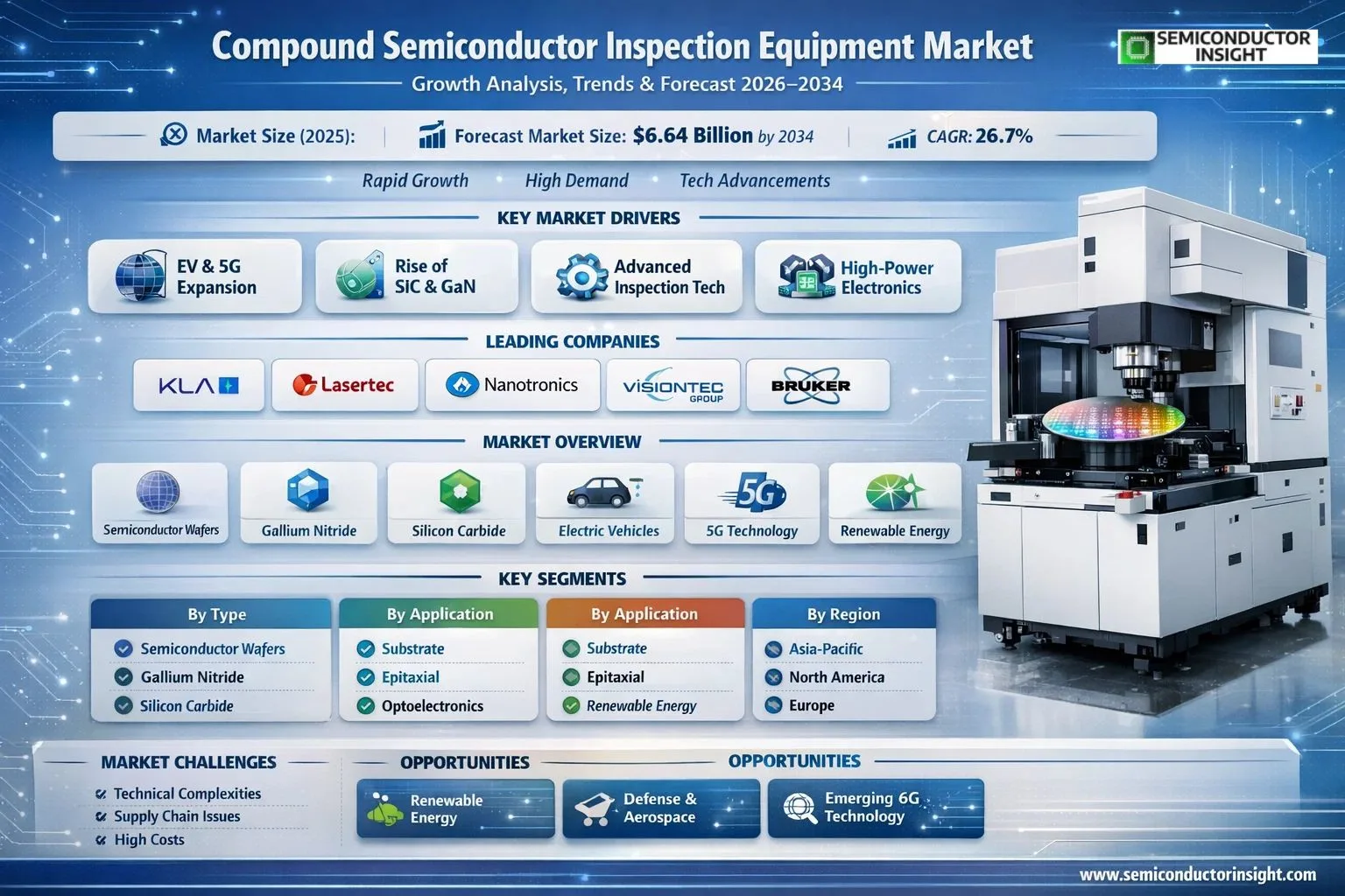
Global Compound Semiconductor Inspection Equipment market size was valued at USD 1.31 billion in 2025. The market is projected to grow from USD 1.66 billion in 2026 to USD 6.64 billion by 2034, exhibiting a CAGR of 26.7% during the forecast period.
Compound semiconductor inspection equipment comprises highly specialized systems designed to detect and classify microscopic defects, particles, scratches, pits, and cracks on wafers made from materials like silicon carbide (SiC) and gallium nitride (GaN). These systems are critical for maintaining high yield in the fabrication of advanced power electronics and optoelectronics, as even nanoscale imperfections can significantly impact the performance and reliability of the final semiconductor devices.
The market is experiencing explosive growth primarily due to the rapid acceleration in automotive electrification. The demand for SiC and GaN power devices, which are key components in electric vehicle (EV) powertrains, onboard chargers, and fast-charging infrastructure, has surged dramatically. This, in turn, drives the need for high-precision inspection systems throughout the manufacturing process to ensure device quality and reliability. Furthermore, advancements in inspection technologies, such as the integration of artificial intelligence for automated defect classification and the development of systems with higher throughput and sensitivity, are contributing significantly to market expansion. Key industry players, including KLA Corporation with its Surfscan® SP series and Lasertec with its SICA platform, are continuously innovating and launching new products to capture this growing demand.
MARKET DRIVERS
Expansion in 5G Infrastructure and Electric Vehicles
Compound Semiconductor Inspection Equipment Market is propelled by surging demand for high-performance materials like gallium nitride (GaN) and silicon carbide (SiC) in 5G base stations and electric vehicle power electronics. These applications require precise defect detection at nanoscale levels to ensure reliability, driving adoption of advanced optical and electron beam inspection systems.
Global 5G deployments have accelerated, with over 1.5 million base stations installed by mid-2023, necessitating robust inspection tools for compound wafers to minimize yield losses exceeding 20% in early production runs.
Innovation in High-Power Electronics
Advancements in compound semiconductor fabrication for RF and power devices further fuel market growth, as manufacturers integrate automated inspection for real-time process control.
➤ The market is projected to expand at a CAGR of 9.2% through 2030, supported by rising EV production targeting 17 million units annually by 2028.
Enhanced metrology capabilities address the shift to 200mm and 300mm wafers, optimizing throughput in high-volume manufacturing environments.
MARKET CHALLENGES
Technical Complexities in Nanoscale Inspection
Inspecting compound semiconductors presents hurdles due to their heterogeneous structures, where traditional silicon tools falter in detecting subsurface defects in materials like GaAs and InP, leading to higher false positives and extended calibration times.
Integration of AI-driven analytics remains inconsistent across fabs, complicating scalability for Compound Semiconductor Inspection Equipment Market as node sizes shrink below 5nm equivalents.
Other Challenges
Supply Chain Disruptions
Geopolitical tensions have increased lead times for rare earth-dependent components, inflating equipment costs by up to 15% in 2023 and delaying market penetration in emerging regions.
Skill gaps in operating sophisticated systems hinder adoption, with training demands outpacing workforce development in key Asian manufacturing hubs.
MARKET RESTRAINTS
High Capital Intensity and Cost Barriers
Compound Semiconductor Inspection Equipment Market faces significant restraints from elevated upfront investments, often exceeding $10 million per advanced toolset, deterring smaller fabs and startups from upgrading legacy systems.
Maintenance expenses for vacuum-based e-beam inspectors add ongoing burdens, with annual costs averaging 20% of purchase price, limiting expansion in cost-sensitive sectors like consumer LEDs.
Compatibility issues with diverse compound materials slow standardization efforts, prolonging ROI periods beyond 3-5 years for many deployments.
MARKET OPPORTUNITIES
Growth in Renewable Energy and Defense Applications
Opportunities abound in solar inverters and radar systems leveraging SiC and GaN, where demand for high-resolution inspection equipment is set to rise with global renewable capacity additions targeting 500 GW annually by 2025.
Emerging 6G R&D initiatives promise further expansion, emphasizing non-destructive testing for next-gen compound devices in Compound Semiconductor Inspection Equipment Market.
Hybrid inspection platforms combining darkfield and laser scattering technologies offer pathways to capture shares in underserved photonics segments, projected to grow 12% yearly.
Compound Semiconductor Inspection Equipment Market Trends
Surge in Demand from Electric Vehicle Electrification
Compound Semiconductor Inspection Equipment Market is experiencing robust growth primarily due to the accelerating electrification of automobiles. As electric vehicles gain widespread adoption, the demand for silicon carbide (SiC) and gallium nitride (GaN) power devices has intensified, positioning these materials as critical components in EV powertrains. Inspection equipment plays a pivotal role in ensuring the quality of SiC and GaN wafers by detecting defects such as particles, scratches, pits, and cracks during production. This trend underscores the market’s alignment with Global shift toward sustainable transportation, where high-reliability semiconductors are essential for efficient power management and thermal performance.
Other Trends
Advancements in High-Precision Inspection Technologies
Leading systems like KLA Corporation’s Surfscan SP Ax and Candela 8520, Lasertec’s SICA88, and Nanotronics’ nSpec PRISM are setting new benchmarks in Compound Semiconductor Inspection Equipment Market with their superior precision and efficiency. These tools enable non-contact detection of microscopic defects on substrates and epitaxial layers, supporting higher yields in SiC and GaN manufacturing. Manufacturers are increasingly investing in automated, AI-enhanced inspection solutions to meet stringent quality standards for power electronics, reducing downtime and enhancing throughput in fabrication facilities.
In the SiC inspection equipment segment, innovations focus on handling larger wafer sizes and complex surface topographies, while GaN systems emphasize real-time monitoring for epitaxial growth uniformity. This technological evolution is driven by industry collaboration among key players including Visiontec Group, TASMIT, Inc., and Bruker, fostering modular designs adaptable to diverse production scales.
Regional Expansion and Competitive Dynamics in Asia-Pacific
Asia-Pacific, particularly China, Japan, and South Korea, dominates Compound Semiconductor Inspection Equipment Market, accounting for a significant portion of global deployments due to concentrated SiC and GaN production capacities. Local firms such as Angkun Vision, Shenzhen Glint Vision, CETC Fenghua, and HGTECH are intensifying competition against established leaders like KLA and Lasertec, offering cost-effective alternatives tailored to regional supply chains. This shift is propelled by government initiatives supporting semiconductor self-sufficiency and the booming EV and renewable energy sectors. In Europe and North America, demand grows steadily from applications in 5G infrastructure and aerospace, though Asia’s scale drives overall market innovation and pricing pressures.
Challenges persist, including supply chain vulnerabilities and the need for skilled operators, yet the outlook remains positive as substrate and epitaxial inspection applications expand into emerging areas like fast-charging systems and high-frequency devices. Strategic mergers and R&D investments among top players signal sustained momentum in this vital niche of the semiconductor ecosystem.
COMPETITIVE LANDSCAPE
Key Industry Players
Dominating Manufacturers in Compound Semiconductor Inspection Equipment
Compound Semiconductor Inspection Equipment Market is led by KLA Corporation, a dominant force with advanced systems like Surfscan SP Ax and Candela 8520, renowned for high precision in detecting defects such as particles, scratches, pits, and cracks on silicon carbide (SiC) and gallium nitride (GaN) wafers. KLA holds a significant market share, driven by surging demand for power devices in electric vehicles and electrification trends. The market structure is moderately concentrated, with top players controlling over 50% of global revenues, while innovation in inspection technologies for substrates and epitaxial layers shapes competitive dynamics amid rapid growth from $1,309 million in 2025 to $6,635 million by 2034 at a 26.7% CAGR.
Beyond KLA, niche players like Lasertec with its SICA88 system and Nanotronics featuring nSpec PRISM contribute specialized solutions, focusing on efficiency for SiC and GaN production challenges. Emerging competitors, particularly from Asia, including TASMIT, Bruker, and various Chinese firms such as Angkun Vision and Shenzhen Glint Vision, are gaining traction through cost-effective innovations and regional supply chain integration. This fragmented tail of the market intensifies competition, pushing advancements in defect detection for automotive and power electronics applications, though leaders maintain edges in scale and R&D.
List of Key Compound Semiconductor Inspection Equipment Companies Profiled
- KLA Corporation
- Lasertec
- Nanotronics
- Visiontec Group
- Bruker
- TASMIT, Inc.
- LAZIN CO.,LTD
- EtaMax
- Spirox Corporation
- Angkun Vision (Beijing) Technology
- Shenzhen Glint Vision
- CETC Fenghua Information Equipment
- CASI Vision Technology (Luoyang) Co., Ltd
- Shanghai Youruipu Semiconductor Equipment
- Dalian Chuangrui Spectral Technology Co., Ltd
Segment Analysis:
| Segment Category | Sub-Segments | Key Insights |
| By Type |
|
SiC Inspection Equipment
|
| By Application |
|
Substrate
|
| By End User |
|
Automotive
|
| By Technology |
|
Laser Scattering
|
| By Deployment |
|
Standalone Systems
|
Regional Analysis: Compound Semiconductor Inspection Equipment Market
Asia-Pacific
Asia-Pacific’s expansive manufacturing landscape underpins Compound Semiconductor Inspection Equipment Market, with key foundries prioritizing defect-free production. Inspection equipment facilitates precise wafer-level analysis, vital for compound materials prone to unique crystalline imperfections. This focus drives adoption of high-resolution imaging systems, optimizing processes across power electronics and photonics sectors.
Innovation thrives in Asia-Pacific, where equipment developers integrate machine learning for real-time anomaly detection in Compound Semiconductor Inspection Equipment Market applications. Tailored solutions address GaN and SiC-specific challenges, enhancing metrology accuracy and reducing false positives, thereby supporting the region’s leadership in advanced semiconductor ecosystems.
Robust supply chains in Asia-Pacific streamline Compound Semiconductor Inspection Equipment Market, enabling swift integration of inspection tools into fab operations. Proximity of suppliers and end-users minimizes disruptions, fostering agile responses to evolving production needs in high-stakes sectors like telecommunications and renewable energy.
Strategic investments and supportive policies accelerate growth in Asia-Pacific’s Compound Semiconductor Inspection Equipment Market. Initiatives fund R&D for next-gen inspection technologies, cultivating partnerships that bridge equipment providers with device manufacturers, ensuring sustained regional dominance.
North America
North America plays a pivotal role in Compound Semiconductor Inspection Equipment Market through its emphasis on cutting-edge R&D and original equipment manufacturing. Leading firms here specialize in developing high-precision inspection systems for compound semiconductors, focusing on applications in defense, aerospace, and telecommunications. The region’s strong intellectual property framework encourages innovation in automated metrology tools, addressing complex defect modes in materials like GaAs and InP. Collaborations between academia and industry drive advancements, while a skilled workforce ensures effective deployment. Though production volumes trail Asia-Pacific, North America’s focus on premium, customized solutions positions it as a quality leader, influencing global standards in Compound Semiconductor Inspection Equipment Market.
Europe
Europe contributes significantly to Compound Semiconductor Inspection Equipment Market with its expertise in precision engineering and automotive applications. Countries like Germany and the UK host developers of advanced inspection platforms tailored for SiC and GaN devices used in electric vehicles and industrial power systems. Emphasis on sustainability integrates eco-friendly inspection processes, minimizing waste in compound semiconductor fabrication. Regulatory standards promote high-reliability tools, fostering trust among manufacturers. Europe’s integrated approach links inspection equipment with broader quality assurance ecosystems, supporting steady market expansion amid rising demand for efficient power electronics.
South America
South America represents an emerging frontier in Compound Semiconductor Inspection Equipment Market, with gradual adoption driven by growing electronics sectors in Brazil and neighboring nations. Initial focus lies on importing inspection tools for nascent compound semiconductor initiatives in renewable energy and consumer devices. Local investments aim to build capabilities, reducing reliance on foreign suppliers. Challenges like infrastructure gaps are offset by international partnerships, introducing foundational metrology systems. This positions South America for measured growth as regional industries mature and integrate advanced inspection practices.
Middle East & Africa
The Middle East & Africa region is nascent yet promising in Compound Semiconductor Inspection Equipment Market, propelled by diversification efforts in the UAE and South Africa. Investments in semiconductor hubs target inspection equipment for power management in oil-to-renewables transitions. Emphasis on training programs builds local expertise, while strategic alliances bring in sophisticated tools for GaN-based systems. Despite infrastructural hurdles, visionary projects signal potential for accelerated uptake, enhancing regional competitiveness in specialized compound semiconductor applications.
Report Scope
This market research report provides a comprehensive analysis of Compound Semiconductor Inspection Equipment Market, covering the forecast period 2026–2034. It offers detailed insights into market dynamics, technological advancements, competitive landscape, and key trends shaping the industry.
Key focus areas of the report include:
- Market Overview: The report begins with an overview outlining its current market scenario, key growth indicators, and industry transformation drivers. It discusses macroeconomic factors, demand–supply balance, regulatory landscape, and the strategic role of semiconductors in powering advancements across industries such as automotive, telecommunications, consumer electronics, and industrial automation.
- Market Size & Forecast: Historical data and future projections for revenue, unit shipments, and market value across major regions and segments.
- Segmentation Analysis: Detailed breakdown by product type, technology, application, and end-user industry to identify high-growth segments and investment opportunities.
- Regional Insights: Insights into market performance across North America, Europe, Asia-Pacific, Latin America, and the Middle East & Africa, including country-level analysis where relevant.
- Competitive Landscape: Profiles of leading market participants, including their product offerings, R&D focus, manufacturing capacity, pricing strategies, and recent developments such as mergers, acquisitions, and partnerships.
- Technology Trends & Innovation: Assessment of emerging technologies, integration of AI/IoT, semiconductor design trends, fabrication techniques, and evolving industry standards.
- Market Drivers & Restraints: Evaluation of factors driving market growth along with challenges, supply chain constraints, regulatory issues, and market-entry barriers.
- Stakeholder Insights: Insights for component suppliers, OEMs, system integrators, investors, and policymakers regarding the evolving ecosystem and strategic opportunities.
Primary and secondary research methods are employed, including interviews with industry experts, data from verified sources, and real-time market intelligence to ensure the accuracy and reliability of the insights presented.
FREQUENTLY ASKED QUESTIONS:
What is the current market size of Compound Semiconductor Inspection Equipment Market?
-> Compound Semiconductor Inspection Equipment Market was valued at USD 1,309 million in 2025 and is expected to reach USD 6,635 million by 2034, at a CAGR of 26.7% during the forecast period.
Which key companies operate in Compound Semiconductor Inspection Equipment Market?
-> Key players include KLA Corporation, Lasertec, Nanotronics, Visiontec Group, and Bruker, among others.
What are the key growth drivers?
-> Key growth drivers include accelerating electrification of automobiles and surging demand for silicon carbide and gallium nitride power devices in electric vehicles.
Which region dominates the market?
-> Asia dominates the market, driven by major countries such as China, Japan, and South Korea.
What are the emerging trends?
-> Emerging trends include high-precision inspection systems for detecting defects like particles, scratches, pits, and cracks in SiC and GaN production.

Get Sample Report PDF for Exclusive Insights
Report Sample Includes
- Table of Contents
- List of Tables & Figures
- Charts, Research Methodology, and more...