
Key Statistics
Key Takeaways
- Soft pads are the leading product type because their controlled compressibility and surface conformity support low-defect polishing across oxide, STI, dielectric and finishing steps where within-wafer uniformity is critical.
- 300 mm wafers are the dominant application because advanced logic, DRAM, 3D NAND and high-volume foundry manufacturing increasingly run on 300 mm platforms, creating the largest recurring consumables demand for polishing pads.
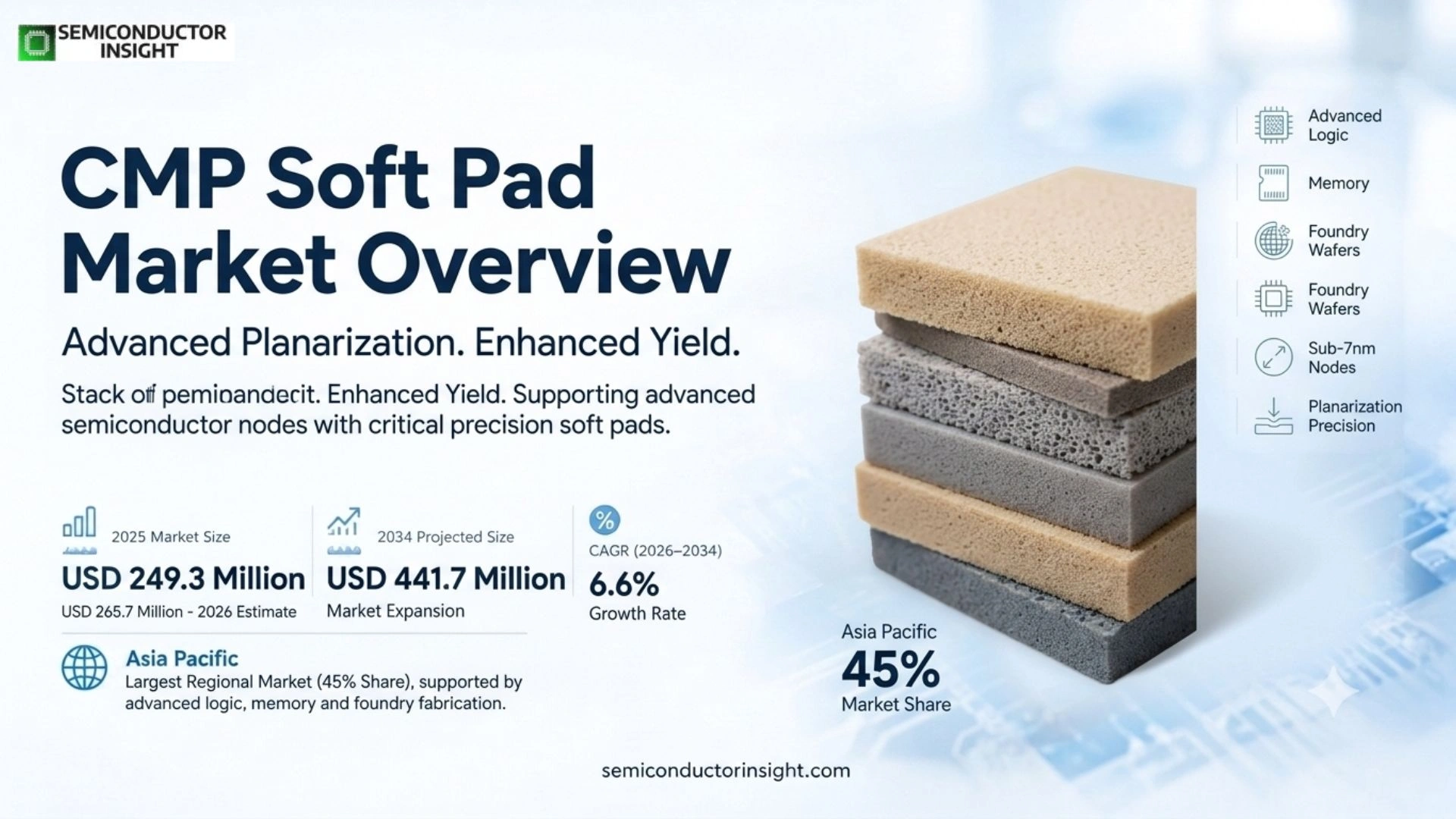
- Asia Pacific is the largest region with a 45% market share, driven by the concentration of semiconductor fabrication in Taiwan, South Korea, China and Japan and the proximity of pad suppliers to high-volume fabs.
- Supplier qualification creates high switching costs. CMP pads are validated together with slurry, conditioner, pressure, platen speed and post-CMP cleaning conditions, so a new pad must prove removal rate, defects, planarization and lifetime before production adoption.
- Advanced nodes are raising performance requirements. TSMC entered 2 nm high-volume manufacturing in 4Q 2025, while SEMI’s Q2 2026 300 mm outlook tracks more than 400 fabs and lines and expects record equipment spending, expanding the process base that consumes CMP pads.
CMP Soft Pad Market Overview
CMP Soft Pad market was valued at USD 249.3 million in 2025 and is projected to reach USD 441.7 million by 2034, representing a 6.6% CAGR during 2026–2034. The 2026 estimated market size is USD 265.7 million. Asia Pacific is the largest region with a 45% market share, supported by the concentration of advanced logic, memory and foundry wafer fabrication.
CMP soft pads are polymer-based consumables used in chemical mechanical planarization to maintain controlled contact between a wafer surface and the polishing slurry. Their mechanical properties influence material removal, within-wafer non-uniformity, dishing, erosion, scratches and defectivity. Unlike a generic polishing surface, a semiconductor CMP pad is engineered around hardness, compressibility, pore structure, groove geometry, surface texture and conditioning response so that process behavior remains stable over many wafers.
Pad performance is inseparable from the rest of the CMP module. The same material can behave differently when paired with another slurry, conditioner disk, platen pressure or wafer pattern density. Fabs therefore qualify pad and slurry combinations using removal rate, selectivity, defect count, endpoint behavior and lifetime. This creates a technically demanding supply relationship in which lot-to-lot consistency and application engineering can matter more than the lowest consumable price.
Demand expands with wafer starts and the number of planarization steps per wafer. Advanced logic, gate-all-around devices, 3D NAND, HBM and heterogeneous integration use repeated material deposition and patterning, increasing the need for tightly controlled surface planarity. At the same time, leading fabs are moving more production to 300 mm and advanced nodes, where the economic value of each wafer makes defect reduction particularly important and supports premium polishing consumables.
Segment Analysis: By Type
By type, the report covers Soft Pad, Adjustable Pad, Composite Pad, Grooved Pad and Others. Soft pads hold the leading position because conformability and controlled compressibility help reduce local defects and improve contact across wafer topography, while adjustable and composite designs address process windows that require more deliberate pressure distribution, stiffness or lifetime control.
| Type | Material / process role | Market position |
|---|---|---|
| Soft Pad | Soft pads use compliant polymer or fiber structures that conform to local wafer topography and distribute contact pressure more gently than harder polishing surfaces. They are well suited to buff, oxide, dielectric and finishing steps where scratch reduction and low defectivity are important. Performance depends on pore structure, pad rebound, slurry transport and conditioning response. | Leading segment. Soft pads are favored in processes where surface quality and planarization consistency are more important than maximum removal aggression. Advanced-node fabs value stable mechanical response because the cost of a scratch or local defect rises sharply as die value increases. |
| Adjustable Pad | Adjustable or tunable pad systems alter effective pressure, compliance or support characteristics to widen the process window across different wafer topographies. They can help compensate for edge effects, pattern-density variation or process drift when a fixed mechanical response is insufficient. | A specialized growth segment. Adoption is strongest in complex processes where fabs are willing to pay for better controllability, but additional hardware, recipe development and qualification can slow deployment relative to conventional pads. |
| Composite Pad | Composite pads combine layers or materials with different hardness, porosity or backing properties. The architecture can provide a firm polishing surface with a compliant sub-pad, allowing suppliers to tune removal efficiency, local contact and vibration behavior independently. | A technically important segment in high-value CMP steps. Composite constructions are useful when one monolithic material cannot deliver both stable removal and low defectivity, but manufacturing consistency across bonded layers is essential. |
| Grooved Pad | Grooved pads use engineered channels to distribute slurry, evacuate debris and control hydrodynamic behavior across the polishing surface. Groove width, pitch, depth and pattern can influence slurry utilization, pad conditioning and local removal behavior. | A design feature that can be sold as a distinct pad category or integrated into soft and composite products. Differentiation comes from combining groove geometry with material chemistry and process-specific conditioner behavior. |
Material composition and end-user segmentation
Demand can also be segmented by material composition and end user. Polyurethane foam is the leading material family because its hardness, pore structure and elastic recovery can be engineered over a broad range. Non-woven fiber and composite systems serve selected finishing and specialty processes. Semiconductor foundries are the largest end-user group because high wafer volumes and frequent advanced-node process changes create recurring demand for qualified consumables and local technical support.
| Axis | Segments | Commercial implication |
|---|---|---|
| By Material Composition | Polyurethane Foam · Non-woven Fibers · Composite Materials · Others | Polyurethane provides the broadest tunability in hardness, porosity and conditioning response. Fiber-based pads support low-defect finishing and specialty applications, while composites combine layers to balance removal efficiency and wafer conformity. |
| By End User | Semiconductor Foundries · Integrated Device Manufacturers · Research & Development Centers | Foundries create the largest recurring consumption because they run high wafer volumes across many customer products. IDMs also maintain large qualified pad sets, while R&D centers purchase lower volumes but influence future material and process requirements. |
Segment Analysis: By Application
By application, 300 mm Wafer polishing is the dominant segment, followed by 200 mm and other wafer sizes. The 300 mm platform concentrates leading-edge logic, DRAM, NAND and large-volume foundry production, so it generates the largest consumables requirement. Mature 200 mm fabs remain important for analog, power, MEMS and specialty semiconductors where long-qualified CMP processes continue to operate.
| Application | Demand characteristics |
|---|---|
| 300 mm Wafer | The dominant application includes leading-edge logic, high-performance computing, DRAM, NAND and advanced foundry production. A 300 mm wafer contains more die and higher economic value than smaller formats, so CMP defects are costly. Fabs therefore emphasize pad uniformity, lifetime, stable conditioning and compatibility with advanced slurries across repeated oxide, metal and dielectric planarization steps. |
| 200 mm Wafer | Mature 200 mm fabs manufacture analog, power, MEMS, sensors and specialty ICs. Their CMP recipes are often long-qualified and stable, which makes suppliers compete on consistency, lifecycle support and cost rather than only the newest material technology. Capacity constraints in 200 mm specialty fabs can sustain healthy pad consumption even when node migration is limited. |
| Other Wafer Sizes | 150 mm and specialty wafer formats remain in compound semiconductor, research and legacy production. Volumes are smaller, but processes can require customized pad hardness, groove design or chemical compatibility. Suppliers with flexible converting and technical support can serve these niches without relying on the largest 300 mm volumes. |
Regional Analysis
Asia Pacific leads the CMP Soft Pad market with a 45% market share. Taiwan, South Korea, China and Japan combine the largest concentration of 300 mm foundry and memory capacity with local materials and consumables suppliers. North America is the second-largest market at 28%, supported by advanced logic, memory and domestic fab expansion. Europe is smaller but technically demanding in automotive and specialty semiconductors.
How do CMP pad demand mechanisms differ across semiconductor manufacturing regions?
CMP pad demand is closely tied to wafer starts and process complexity rather than to downstream electronics consumption. Asia Pacific leads because the region contains the deepest front-end semiconductor manufacturing base. North America is expanding advanced-node and memory capacity, Europe emphasizes automotive and specialty technologies, and emerging regions remain smaller until new wafer-fabrication projects move from construction into production.
| Region | Market position | Growth outlook | Demand profile | What decides supplier selection |
|---|---|---|---|---|
| Asia Pacific | Largest, 45% share | High | Foundry & memory | Local support, yield and advanced-node qualification |
| North America | Second, 28% source share | High | Logic, memory & R&D | Defect control, process IP and supply assurance |
| Europe | Specialized | Moderate | Automotive & industrial | Lifecycle, sustainability and reliability |
| South America | Small | Selective | Specialty & imported materials | Logistics and technical support |
| Middle East & Africa | Emerging | Selective | New semiconductor investment | Fab ramp timing and qualified imports |
Competitive Landscape
Key participants include DuPont, CMC Materials, FUJIBO, IVT Technologies, TWI Incorporated, 3M, Dow Chemical, AGC and Shin-Etsu Chemical. The competitive structure is moderately concentrated because advanced CMP pads require proprietary polymer formulation, precision manufacturing, grooving, surface finishing and extensive fab qualification. Current industry ownership has changed in parts of the landscape, with Qnity now carrying major semiconductor CMP pad technology formerly associated with DuPont Electronics and CMC Materials integrated into Entegris.
DuPont’s IC1000 family established a long-running industry benchmark for CMP pads across copper, tungsten, STI/ceria, oxide and buff applications. In the current market, Qnity Electronics is expanding the product line with Optivision Max, launched in June 2026 for advanced nodes and evolving device architectures. The competitive advantage is not a single pad chemistry but a broad materials portfolio, application data and deep qualification history across leading fabs.
Entegris combines the former CMC Materials portfolio with a wider contamination-control and semiconductor materials business. This creates opportunities to coordinate slurry, pad, filtration and post-CMP process support around customer defect goals. FUJIBO and Japanese specialty suppliers compete through precision polymer and textile technologies, while regional Asian companies can use local fab proximity and fast customization to win specific process steps.
Supplier concentration is reinforced by qualification cost. Fabs are reluctant to change a pad that already delivers stable yield unless a new product offers a clear improvement in defectivity, lifetime, removal rate or cost of ownership. This favors vendors with strong on-site application engineering, quality systems and the manufacturing scale to reproduce pad properties across many lots.
Competitive tier structure
| Tier | Companies | Basis of competition |
|---|---|---|
| Global platform suppliers | DuPont / Qnity; CMC Materials / Entegris; FUJIBO | Broad pad portfolios, deep fab qualifications, advanced-node R&D and global technical support |
| Materials & specialty suppliers | 3M; Dow Chemical; AGC; Shin-Etsu Chemical | Polymer, chemical and precision-material capabilities supporting selected CMP applications and adjacent process materials |
| Regional specialists | IVT Technologies; TWI Incorporated | Customized pad structures, local customer support and niche process targeting |
Key companies profiled in the report scope
- DuPont de Nemours, Inc. / Qnity Electronics
- CMC Materials, Inc. / Entegris
- FUJIBO Holdings
- IVT Technologies Co., Ltd.
- TWI Incorporated
- 3M Company
- Dow Chemical Company
- AGC Inc.
- Shin-Etsu Chemical Co., Ltd.
CMP Soft Pad Production Capacity & Supply-Side Analysis
CMP pad capacity depends on polymer formulation, foaming or fiber processing, casting, curing, precision thickness control, grooving, surface finishing, inspection and clean packaging. Physical factory output is only one part of usable capacity because semiconductor customers require tight lot-to-lot consistency and qualified formulations. A supplier can expand production faster than it can expand approved customer volume if new lines or raw-material changes require requalification.
Pad manufacturing must control hardness, compressibility, pore size, groove geometry and thickness across large production lots. Small shifts can change slurry transport, contact pressure or conditioning rate and alter wafer removal behavior. Statistical process control and traceability are therefore essential. Suppliers also need converting flexibility because different customers may use unique diameters, grooves or sub-pad constructions even when the core polymer formulation is similar.
Regional inventory near fabs can be as important as central manufacturing. Pads are recurring consumables, and a shortage can interrupt wafer production even if every tool is operational. Large suppliers maintain local technical and logistics support in Taiwan, Korea, Japan, China and the United States, while emerging suppliers often partner with distributors. The best supply position combines qualified global manufacturing with local stock and engineers who can respond to process excursions.
Market Dynamics
Growth is driven by 300 mm capacity expansion, advanced-node logic, HBM and 3D NAND, more CMP steps per wafer and advanced packaging. Restraints include long qualification cycles, strict consistency requirements, specialty polymer cost and process substitution in selected steps. Opportunities center on low-defect soft pads, sustainable materials, smart conditioning and packaging-related planarization.
MARKET DRIVERS
Drivers Impact Analysis*
| Factor | Forecast impact* | Geographic relevance | Impact timeline |
|---|---|---|---|
| 300 mm fab capacity expansion | High | Asia Pacific, North America | Medium to long term |
| Advanced-node process complexity | High | Leading-edge fabs | Persistent |
| HBM / 3D NAND scaling | Medium to high | Korea, Taiwan, China, U.S. | Medium term |
| Advanced packaging planarization | Medium | Global packaging hubs | Medium to long term |
*Directional analytical rating; it is not a measured contribution to the headline CAGR.
300 mm capacity expands recurring consumables demand
SEMI’s 2026 outlook shows sustained investment in 300 mm fabs driven by AI, high-performance computing and memory. Once a new line reaches production, every qualifying CMP step consumes pads continuously. This creates a recurring revenue stream tied to wafer starts and tool utilization rather than the one-time capital purchase of the CMP equipment itself.
Advanced nodes tighten defect budgets
Leading-edge transistors and dense interconnect stacks require flatter surfaces and more precise material removal. A scratch, particle or local non-uniformity can destroy expensive die, so fabs place greater value on stable pad texture, controlled compliance and predictable conditioning. This shifts purchasing toward proven high-performance pads even when they cost more per unit.
Memory architectures add repeated polishing steps
3D NAND, advanced DRAM and HBM create complex stacks of oxide, metal and dielectric materials. Higher layer counts and advanced memory packaging can increase the number and difficulty of CMP operations. Suppliers that support several material systems with compatible soft-pad platforms can capture more consumable value per wafer.
Advanced packaging creates new process surfaces
Hybrid bonding, TSV reveal and heterogeneous integration require extremely flat interfaces before dies or wafers are bonded. These steps can need different mechanical behavior from front-end CMP. Pad companies that co-develop products with slurry and packaging customers can extend beyond traditional STI, oxide and metal applications.
MARKET RESTRAINTS
Restraints Impact Analysis*
| Factor | Forecast impact* | Geographic relevance | Impact timeline |
|---|---|---|---|
| Long fab qualification cycles | High | Global | Persistent |
| Batch consistency requirements | High | Advanced fabs | Persistent |
| Specialty polymer cost | Medium | Global supply chain | Short to medium term |
| Alternative planarization approaches | Low to medium | Process-specific | Long term |
*Directional analytical rating; it is not a measured contribution to the headline CAGR.
Qualification slows supplier switching
A new pad must be tested with the customer’s slurry, conditioner, tool settings and wafer patterns. Fabs evaluate removal rate, non-uniformity, defects, lifetime and downstream yield before approving production. The process can take months, which creates high barriers for new entrants and delays revenue even when a product performs well in laboratory tests.
Manufacturing variation can create yield risk
Pad hardness, pore distribution, groove dimensions and thickness influence process behavior. If a manufacturing lot drifts, wafer defects or removal rate can change before the root cause is obvious. Suppliers therefore carry high quality-control costs and fabs may require detailed change notification before a raw material, line or manufacturing location is modified.
Advanced polymers and precision conversion increase cost
High-performance pads use engineered polyurethane, fibers, fillers and proprietary manufacturing steps. Precision grooving, surface finishing and clean packaging add more cost. Cost-sensitive fabs or mature processes may resist premium products unless the supplier can demonstrate longer pad life, lower slurry use or better yield.
Some process changes can reduce mechanical polishing intensity
Deposition, etch, bonding and process integration improvements can reduce the amount of CMP required in selected steps. These technologies are not a broad replacement for planarization, but they can change pad demand within a process flow. Suppliers must therefore follow device architecture and packaging roadmaps rather than extrapolating pad consumption only from wafer volume.
MARKET OPPORTUNITIES
Launch lower-defect pads for sub-2 nm logic
New gate-all-around nodes demand very tight planarity and defect control. Suppliers can target low-scratch soft pads with controlled pore structures and conditioning behavior for oxide, dielectric and metal finishing. The strongest commercial proposition is a measurable yield or lifetime improvement validated on customer wafers rather than a generic material claim.
Develop more sustainable pad materials
Semiconductor manufacturers are reducing waste and seeking lower-impact consumables. Longer pad lifetime, recyclable packaging, lower-solvent processing and alternative polymer chemistries can reduce environmental burden. A sustainable pad must still match incumbent defect and removal performance, so materials innovation needs to be qualified as part of the full CMP process.
Integrate pad, conditioner and process analytics
Pad wear changes surface texture and removal behavior over time. Suppliers can add conditioning guidance, lifetime models or sensor data that help fabs predict when performance will drift. Digital process support can strengthen customer relationships and reduce waste by replacing pads based on actual process condition rather than conservative fixed intervals.
Expand into advanced packaging CMP
Hybrid bonding, TSV and interposer processes create new planarization surfaces and wafer forms. These applications may require softer contact, different grooves or new sub-pad constructions. Suppliers that engage early with packaging houses and foundries can establish qualifications before volume production and secure long product cycles.
CMP Soft Pad Supply Chain Analysis
Raw-material consistency sets the mechanical baseline
Polyurethane resin, fillers, fibers and additives influence hardness, rebound, porosity and chemical stability. Suppliers need qualified raw materials and change control because a subtle feedstock shift can alter polishing behavior. Backing layers and adhesives also matter because they influence pad compressibility and mechanical coupling to the platen.
Manufacturing converts chemistry into repeatable geometry
Foaming, casting, curing and fiber processing determine pore structure and bulk mechanics, while grooving and surface finishing control slurry flow and initial pad texture. Precision thickness and flatness are essential because non-uniform pad geometry can translate into wafer non-uniformity. Automated inspection and statistical process control improve consistency across lots.
Qualification creates the commercial barrier to entry
A pad supplier must prove performance on the customer’s actual CMP process. Removal rate alone is insufficient; fabs examine defects, selectivity, dishing, erosion, conditioning, lifetime and cleanability. The cost of this testing means customers tend to limit the number of qualified products, favoring suppliers that can support engineering trials quickly.
Wafer yield determines total pad value
A pad is inexpensive relative to the value of the wafers it polishes. Fabs will pay more for a product that reduces scratches, improves uniformity or extends lifetime without increasing slurry consumption. This yield leverage makes technical support and consistency central to supplier economics and helps explain why established products can remain qualified for many years.
Recent Developments in the CMP Soft Pad Market
Qnity launches Optivision Max CMP pad family
Qnity Electronics expanded its CMP offering with Optivision Max polishing pads designed to improve process control and yield across advanced nodes and evolving semiconductor device architectures. The launch shows continued product investment in engineered pad materials for tighter process windows.
SEMI updates global 300 mm fab outlook
SEMI’s Q2 2026 300 mm Fab Outlook tracks more than 400 fabs and lines and identifies AI, HPC and automotive demand as major investment drivers. Expanding 300 mm capacity increases the long-term installed base of CMP tools and recurring consumables demand.
TSMC moves 2 nm into high-volume manufacturing
TSMC reported that its 2 nm technology entered high-volume manufacturing in the fourth quarter of 2025 and expects a fast ramp in 2026. More advanced process structures increase the importance of tight surface planarity and low-defect CMP consumables.
SEMI forecasts strong advanced-node capacity growth
SEMI projected global 7 nm-and-below capacity to reach 1.4 million wafers per month by 2028, up 69% from 2024. Advanced-node capacity growth supports demand for higher-performance CMP pads and related process materials.
REPORT SCOPE & SEGMENTATION
| Attribute | Details |
|---|---|
| Study Period | 2020–2034 |
| Base Year | 2025 |
| Estimated Year | 2026 |
| Forecast Period | 2026–2034 |
| Historical Period | 2020–2025 |
| Market Size 2025 | USD 249.3 million |
| Market Size 2034 | USD 441.7 million |
| Growth Rate | CAGR of 6.6% from 2026–2034 |
| Unit | Value (USD Million) and pad unit consumption where applicable |
| Segmentation | By Type, By Application, By End User, By Material Composition, By Region |
| By Type | Soft Pad · Adjustable Pad · Composite Pad · Grooved Pad · Others |
| By Application | 300mm Wafer · 200mm Wafer · Other Wafer Sizes |
| By End User | Semiconductor Foundries · Integrated Device Manufacturers · Research & Development Centers |
| By Material Composition | Polyurethane Foam · Non-woven Fibers · Composite Materials · Others |
| By Region | Each region analysed by pad type, wafer size, end user, material composition and country semiconductor ecosystemNorth AmericaUnited States, Canada, MexicoEuropeGermany, France, United Kingdom, Italy, Nordics and other European marketsAsia PacificChina, Taiwan, South Korea, Japan, India, Southeast Asia and other Asian marketsSouth AmericaBrazil, Argentina and other South American marketsMiddle East & AfricaIsrael, Saudi Arabia, UAE, South Africa and other MEA markets |
| Key Companies Profiled | DuPont de Nemours, Inc. / Qnity Electronics · CMC Materials, Inc. / Entegris · FUJIBO Holdings · IVT Technologies Co., Ltd. · TWI Incorporated · 3M Company · Dow Chemical Company · AGC Inc. · Shin-Etsu Chemical Co., Ltd. |
| Customization Scope | Free report customization equivalent to up to four analyst working days with purchase. Addition or alteration to country, regional and segment scope. |
Frequently Asked Questions
What is the 2025 size of the CMP Soft Pad market?
The market size is USD 249.3 million in 2025 and is projected to reach USD 441.7 million by 2034. The 2026 estimate is USD 265.7 million and the 2026–2034 CAGR is 6.6%. Growth is supported by expanding 300 mm wafer capacity, more demanding advanced-node CMP steps and broader use of high-performance polishing consumables.
What is the long-term growth outlook for CMP Soft Pads?
The market is expected to expand at a 6.6% CAGR during 2026–2034 as wafer starts increase and advanced logic, memory and packaging processes demand tighter planarization control. Growth is strongest where 300 mm production, advanced-node manufacturing and additional CMP steps per wafer raise recurring consumption of qualified pads.
Which CMP pad type leads the market?
Soft pads lead because their compliant mechanical response helps control local wafer contact, reduce scratching and support low-defect finishing across oxide, STI and dielectric applications. Adjustable and composite pads serve more specialized requirements where fabs need additional control over pressure distribution, stiffness, lifetime or process stability.
Which application is the largest?
The 300 mm wafer segment is the largest because leading-edge logic, DRAM, NAND and high-volume foundry manufacturing are concentrated on 300 mm platforms. Continued capacity expansion increases the recurring consumption of CMP pads once new lines enter production, while the high value of advanced wafers increases willingness to pay for low-defect consumables.
Which region leads in 2025?
Asia Pacific leads with a 45% market share. Taiwan, South Korea, China and Japan combine the world’s deepest concentration of wafer fabrication, memory manufacturing and semiconductor materials suppliers. North America is the second-largest source region with 28% share and is expanding through new domestic fab investment.
What are the main growth drivers?
The strongest drivers are expansion of 300 mm fab capacity, migration to advanced logic nodes, growth in HBM and 3D NAND, more planarization steps per wafer and new advanced-packaging CMP requirements. Each factor increases either wafer volume, process-step count or the performance value of low-defect pads.
What are the main restraints?
The main restraints are long fab qualification cycles, strict lot-to-lot consistency requirements, specialty polymer and conversion cost, and the possibility that process-integration changes reduce CMP intensity in selected steps. Pad suppliers must prove repeatable yield performance before a fab will accept a new material.
How does a CMP pad affect wafer yield?
Pad hardness, compressibility, porosity, grooves and surface texture influence slurry transport and local contact pressure. Those properties affect removal rate, within-wafer uniformity, scratches, dishing and erosion. Because the pad works together with slurry, conditioner and tool settings, stable manufacturing and application-specific qualification are essential to maintaining production yield.
What opportunity does advanced packaging create?
Hybrid bonding, TSV reveal, interposers and 3D integration create additional surfaces that must be planar before bonding or redistribution. These processes can require different pad compliance and groove structures from front-end wafer CMP, giving suppliers an opportunity to develop packaging-specific soft and composite pad systems.
What does the report cover?
The report covers soft, adjustable, composite, grooved and other pads; 300 mm, 200 mm and other wafer applications; foundries, IDMs and R&D centers; polyurethane, non-woven and composite materials; five global regions; production and supply analysis; and the full profiled company set.
Research Sources & Evidence Base
View primary and authoritative evidence used in this overview
- Qnity Electronics. Optivision Max CMP Pad Family – June 2026 product release on next-generation polishing pads for advanced semiconductor nodes and evolving device architectures.
- DuPont. IC1000 CMP Pads – Product evidence covering long-running CMP pad applications including copper, tungsten, STI/ceria, oxide and buff.
- SEMI. 300mm Fab Outlook – Q2 2026 – Industry evidence on global 300 mm fab investment, capacity and AI-driven manufacturing expansion.
- TSMC. 2025 Annual Report – Primary foundry evidence on 3 nm revenue share, 2 nm high-volume manufacturing and ongoing advanced-fab investment.
- SEMI. Advanced Chipmaking Capacity Outlook – Industry data on projected growth of 7 nm-and-below capacity and leading-edge manufacturing investment.
Get Sample Report PDF for Exclusive Insights
Report Sample Includes
- Table of Contents
- List of Tables & Figures
- Charts, Research Methodology, and more...





