Chiplet interconnect UCIe physical layer jitter budget Market Insights
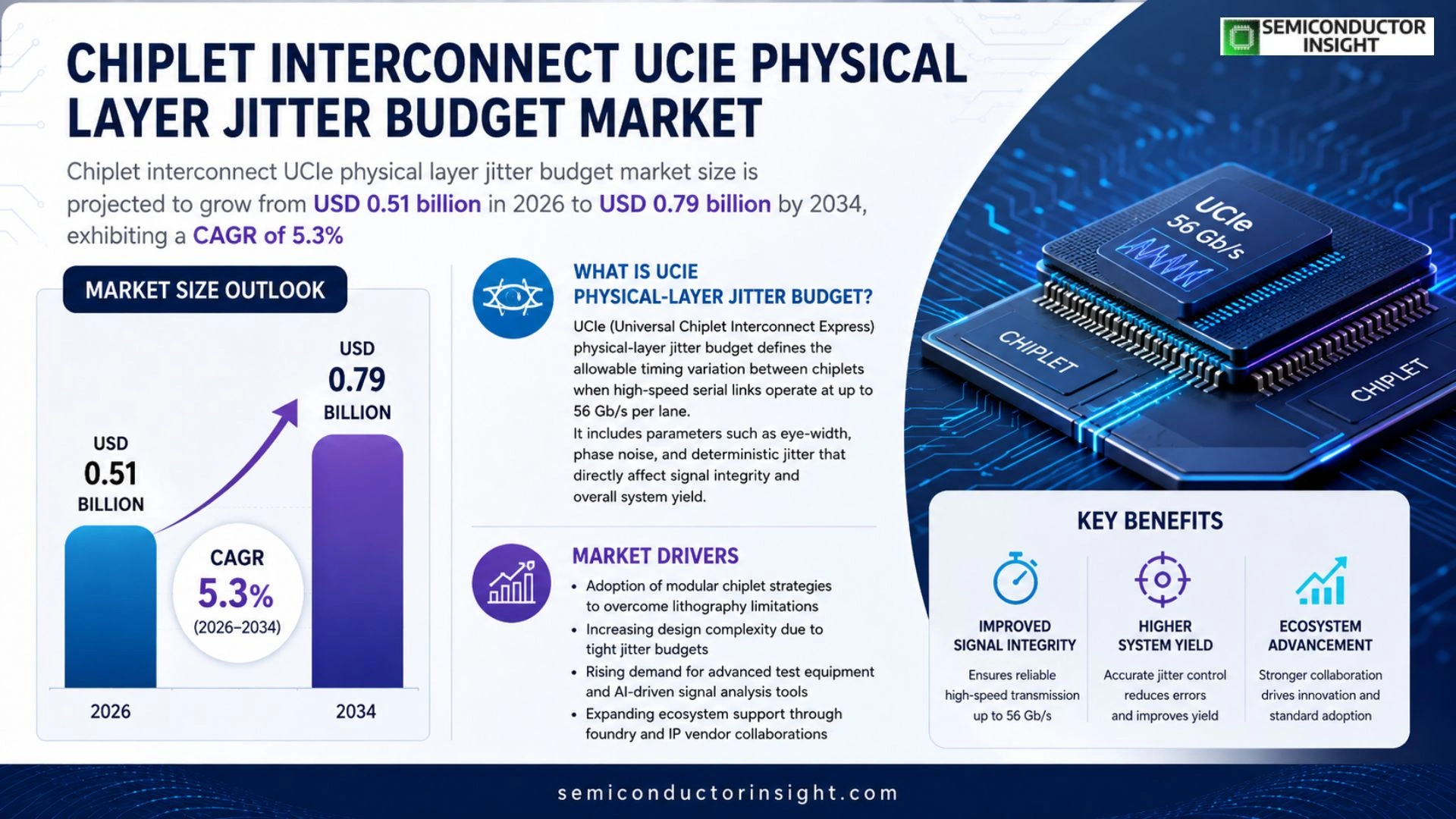
Global Chiplet interconnect UCIe physical layer jitter budget market size was valued at USD 0.46 billion in 2025. The market is projected to grow from USD 0.51 billion in 2026 to USD 0.79 billion by 2034, exhibiting a CAGR of 5.3% during the forecast period.
UCIe (Universal Chiplet Interconnect Express) physical‑layer jitter budget defines the allowable timing variation between chiplets when high‑speed serial links operate at up to 56 Gb/s per lane. It includes parameters such as eye‑width, phase noise, and deterministic jitter that directly affect signal integrity and overall system yield.
The market is accelerating because semiconductor firms are adopting modular chiplet strategies to bypass lithography constraints. However, tight jitter budgets create design complexity, prompting increased spending on advanced test equipment and AI‑driven signal analysis tools. Furthermore, recent collaborations announced by major foundries and IP vendors in early 2024 are expanding ecosystem support, further driving demand for compliant UCIe solutions.
MARKET DRIVERS
Rising Demand for Heterogeneous Compute
The surge in AI‑driven workloads and high‑performance computing is compelling designers to adopt chiplet architectures that can mix CPU, GPU, and accelerator dies. UCIe (Universal Chiplet Interconnect Express) provides a standardized physical layer, enabling faster time‑to‑market while maintaining signal integrity. This trend directly expands Chiplet interconnect UCIe physical layer jitter budget Market as OEMs prioritize low‑jitter connections to meet sub‑nanosecond latency targets.
Standardization Accelerates Ecosystem Growth
Industry consortia such as OCP and JEDEC have ratified the UCIe 1.0 specification, giving silicon vendors a clear roadmap. The resulting design reuse reduces NRE costs, and the predictable jitter budget lowers verification effort, driving broader market adoption across data center and edge devices.
➤ “Designs that meet the UCIe jitter budget can achieve up to 30% higher bandwidth efficiency compared with legacy interconnects.”
As manufacturers scale production, economies of scale further compress component pricing, reinforcing a virtuous cycle that sustains growth in Chiplet interconnect UCIe physical layer jitter budget Market.
MARKET CHALLENGES
Complex Signal Integrity Management
Achieving the stringent jitter budget requires meticulous PCB layout, advanced clock distribution, and high‑precision testing equipment. Many midsize fabs lack the expertise to validate UCIe links at the required picosecond resolution, creating a skill gap that slows adoption.
Other Challenges
Design Tool Integration
Existing EDA suites are still integrating full UCIe models, leading to fragmented simulation flows and longer design cycles.
MARKET RESTRAINTS
High Initial Capital Expenditure
Implementing a compliant physical layer demands specialized test hardware and upgraded manufacturing lines. The upfront cost can be prohibitive for low‑volume players, restraining market penetration despite the long‑term benefits of reduced jitter.
MARKET OPPORTUNITIES
Emerging Edge AI Applications
Edge devices that require real‑time inference are increasingly adopting chiplet solutions to balance performance and power. These deployments demand precise jitter control to maintain deterministic timing, opening a rapid growth corridor for vendors that can deliver validated UCIe physical‑layer solutions.
Chiplet interconnect UCIe physical layer jitter budget Market Trends
Growing Adoption of Modular Chiplet Architectures
Chiplet interconnect UCIe physical layer jitter budget market is experiencing a clear shift toward modular chiplet designs as semiconductor manufacturers seek to extend Moore’s Law without relying on smaller process nodes. By integrating pre‑qualified IP blocks, companies can shorten time‑to‑market while managing the stringent timing tolerances required for high‑speed serial links up to 56 Gb/s per lane. Recent ecosystem agreements announced in early 2024, where leading foundries and IP vendors committed to co‑develop validated UCIe PHY blocks and reference designs, lower entry barriers for smaller fabless firms. This collaborative environment encourages broader participation and sustains demand for compliant jitter‑budget solutions across compute, networking, and AI acceleration segments.
Other Trends
Design Complexity and Jitter Management
Design teams face increasing complexity as jitter budgets tighten to preserve eye‑width and minimize deterministic jitter at multi‑gigahertz frequencies. Advanced test equipment capable of sub‑picosecond resolution is becoming a standard investment, and AI‑driven signal analysis tools are being deployed to accelerate root‑cause identification. These technology adoptions help maintain high yield rates despite the tighter margins imposed by Chiplet interconnect UCIe physical layer jitter budget market, enabling manufacturers to meet performance targets without excessive redesign cycles.
Ecosystem Expansion and AI‑Driven Validation
Beyond hardware, the market is benefiting from an expanding ecosystem of software, verification IP, and design‑for‑test methodologies that address jitter budgeting early in the design flow. Machine‑learning models trained on large datasets of signal integrity measurements are now used to predict jitter impacts of layout variations, reducing the need for extensive physical prototyping. This shift toward predictive validation shortens development timelines and aligns with the strategic objectives of Chiplet interconnect UCIe physical layer jitter budget market, reinforcing its role as a catalyst for next‑generation system‑on‑chip solutions.
COMPETITIVE LANDSCAPE
Key Industry Players
Chiplet Interconnect UCIe Physical Layer Jitter Budget Market Overview
UCIe jitter‑budget ecosystem is presently anchored by a few vertically integrated semiconductor giants that control both silicon design and advanced packaging. Intel leads the market through its extensive portfolio of UCIe‑compliant silicon‑interposer solutions and its proprietary test‑equipment platforms that target the sub‑50 ps jitter envelope required for 56 Gb/s lanes. AMD, following its acquisition of Xilinx, has accelerated its chiplet strategy and now offers a broad range of UCIe IP blocks, positioning itself as a direct competitor to Intel in high‑performance compute segments. Foundry powerhouses such as TSMC and Samsung reinforce the structure by providing the advanced process nodes and interposer technologies that enable tight jitter control, while their joint IP programs with Intel and AMD expand the overall ecosystem. The market structure therefore reflects a dual‑layer model: leading IP vendors drive specification compliance, and leading foundries supply the manufacturing capability, creating a high barrier to entry for new entrants.
Beyond the dominant trio, a vibrant cohort of niche and specialist players adds depth to the competitive landscape. Qualcomm leverages its RF‑centric expertise to develop low‑power UCIe links for mobile and edge applications. NXP and Broadcom focus on automotive and networking segments, offering customized jitter‑budget analytics tools. Synopsys and Cadence provide simulation and verification suites that are essential for meeting deterministic jitter limits. IBM’s research arm contributes advanced signal‑integrity methodologies, while Rapid Silicon and GlobalFoundries deliver silicon‑prototyping services that accelerate time‑to‑market for emerging chiplet designs. Marvell’s data‑center portfolio, together with Arm’s IP frameworks, completes a diversified ecosystem that supports both high‑volume and boutique chiplet solutions.
List of Key Chiplet Interconnect UCIe Physical Layer Jitter Budget Companies Profiled
- Intel Corporation
- Advanced Micro Devices (AMD)
- Taiwan Semiconductor Manufacturing Company (TSMC)
- Samsung Electronics
- Qualcomm Incorporated
- NXP Semiconductors
- Broadcom Inc.
- Synopsys, Inc.
- Cadence Design Systems
- IBM Research
- Rapid Silicon
- GlobalFoundries
- Marvell Technology Group
- Arm Ltd.
- Xilinx (now part of AMD)
Segment Analysis:
| Segment Category | Sub-Segments | Key Insights |
| By Type |
|
High‑Performance Computing Chiplets
|
| By Application |
|
Data‑Center Accelerators
|
| By End User |
|
Semiconductor Foundries
|
| By Design Methodology |
|
Modular Co‑Design
|
| By Validation Tooling |
|
AI‑Driven Jitter Analyzers
|
Regional Analysis: North America
North America is witnessing a surge in the adoption of chiplet designs to overcome performance limitations of monolithic chips. This is particularly evident in the data center sector where the demand for higher bandwidth and lower power consumption is paramount. Companies are increasingly exploring and implementing UCIe to facilitate seamless communication between chiplets, thereby optimizing overall system performance and addressing challenges related to physical layer jitter budget.
The primary drivers for Chiplet interconnect UCIe physical layer jitter budget Market in North America include the growing complexity of electronic systems, the need for improved scalability, and the relentless pursuit of higher performance metrics. Government initiatives supporting semiconductor manufacturing and R&D further fuel market expansion. The focus on energy efficiency also plays a crucial role in driving innovation within this domain.
Despite strong growth prospects, the market faces challenges related to the complexity of chiplet design and manufacturing, standardization efforts, and the need for robust testing and validation methodologies to ensure reliable performance, particularly concerning physical layer jitter budget. Supply chain disruptions have also presented temporary restraints.
The future outlook for Chiplet interconnect UCIe physical layer jitter budget Market in North America remains highly positive. Continued innovation in UCIe technology, coupled with increasing adoption across various applications, is expected to drive significant market growth in the coming years. The region’s strong research capabilities and collaborative ecosystem will be instrumental in shaping future trends.
North America
The North American market for Chiplet interconnect UCIe physical layer jitter budget is experiencing robust growth, propelled by the dynamic data center landscape and advancements in high-performance computing. The region’s substantial investment in semiconductor innovation is a key factor in the development and adoption of these advanced interconnect solutions. Many leading technology companies are strategically based here, fostering a collaborative environment that accelerates technological advancements. The increasing need for bandwidth and reduced latency in applications like artificial intelligence and machine learning is further fueling the demand for UCIe technology. The emphasis on energy efficiency within data centers also aligns with the benefits offered by chiplet designs.
Europe
Europe represents a significant and steadily growing market for Chiplet interconnect UCIe physical layer jitter budget. Driven by strong industrial sectors, including automotive and industrial automation, the demand for higher-performance computing and connectivity is increasing. European initiatives focused on strengthening the domestic semiconductor industry are also providing a boost to the market. While adoption may be slightly less rapid than in North America, Europe is actively investing in research and development to remain competitive in this evolving field. The focus on power efficiency and reliability is particularly prominent in European applications.
Asia-Pacific
Asia-Pacific is emerging as the fastest-growing market for Chiplet interconnect UCIe physical layer jitter budget. Fueled by rapid expansion in the telecommunications, consumer electronics, and industrial sectors, the demand for advanced interconnect solutions is surging. Countries like China, Japan, and South Korea are major contributors to this growth, with significant investments being made in semiconductor manufacturing and research. The increasing adoption of 5G and the growing demand for edge computing are further driving market expansion. The focus on cost-effectiveness and scalability is a key consideration in this region.
South America
South America presents a relatively nascent but promising market for Chiplet interconnect UCIe physical layer jitter budget. The growth is primarily being driven by the expansion of the telecommunications infrastructure and increasing adoption of cloud computing services. While the overall market size is smaller compared to other regions, the potential for growth is significant, particularly in countries with developing technology sectors. Government initiatives aimed at promoting digital transformation are expected to further stimulate market demand.
Middle East & Africa
The Middle East & Africa region is an emerging market for Chiplet interconnect UCIe physical layer jitter budget, with growth being driven by investments in infrastructure development and the increasing adoption of digital technologies. The expansion of data centers and the growing demand for high-performance computing are key factors propelling market expansion. The region’s focus on technological advancement and its growing connectivity initiatives are expected to create favorable opportunities for Chiplet interconnect UCIe physical layer jitter budget Market.
Report Scope
This market research report provides a comprehensive analysis of the Chiplet interconnect UCIe physical layer jitter budget Market , covering the forecast period 2026–2034. It offers detailed insights into market dynamics, technological advancements, competitive landscape, and key trends shaping the industry.
Key focus areas of the report include:
- Market Overview: The report begins with an overview outlining its current market scenario, key growth indicators, and industry transformation drivers. It discusses macroeconomic factors, demand–supply balance, regulatory landscape, and the strategic role of semiconductors in powering advancements across industries such as automotive, telecommunications, consumer electronics, and industrial automation.
- Market Size & Forecast: Historical data and future projections for revenue, unit shipments, and market value across major regions and segments.
- Segmentation Analysis: Detailed breakdown by product type, technology, application, and end-user industry to identify high-growth segments and investment opportunities.
- Regional Insights: Insights into market performance across North America, Europe, Asia-Pacific, Latin America, and the Middle East & Africa, including country-level analysis where relevant.
- Competitive Landscape: Profiles of leading market participants, including their product offerings, R&D focus, manufacturing capacity, pricing strategies, and recent developments such as mergers, acquisitions, and partnerships.
- Technology Trends & Innovation: Assessment of emerging technologies, integration of AI/IoT, semiconductor design trends, fabrication techniques, and evolving industry standards.
- Market Drivers & Restraints: Evaluation of factors driving market growth along with challenges, supply chain constraints, regulatory issues, and market-entry barriers.
- Stakeholder Insights: Insights for component suppliers, OEMs, system integrators, investors, and policymakers regarding the evolving ecosystem and strategic opportunities.
Primary and secondary research methods are employed, including interviews with industry experts, data from verified sources, and real-time market intelligence to ensure the accuracy and reliability of the insights presented.
FREQUENTLY ASKED QUESTIONS:
What is the current market size of Chiplet interconnect UCIe physical layer jitter budget Market?
-> Chiplet interconnect UCIe physical layer jitter budget market is projected to grow from USD 0.51 billion in 2026 to USD 0.79 billion by 2034.
Which key companies operate in Chiplet interconnect UCIe physical layer jitter budget Market?
-> Key players include TSMC, Intel, AMD, Arm, Synopsys, and Cadence, among others.
What are the key growth drivers?
-> Key growth drivers include adoption of modular chiplet strategies, need to bypass lithography constraints, and increasing demand for high‑speed serial links up to 56 Gb/s per lane.
Which region dominates the market?
-> Asia‑Pacific leads the market due to its extensive semiconductor manufacturing base, while North America remains a significant contributor.
What are the emerging trends?
-> Emerging trends include AI‑driven signal analysis tools, advanced test equipment for jitter budgeting, and expanding ecosystem collaborations announced in early 2024.

Get Sample Report PDF for Exclusive Insights
Report Sample Includes
- Table of Contents
- List of Tables & Figures
- Charts, Research Methodology, and more...