Chip-level EMI shielding with conformal copper sputtering Market Insights
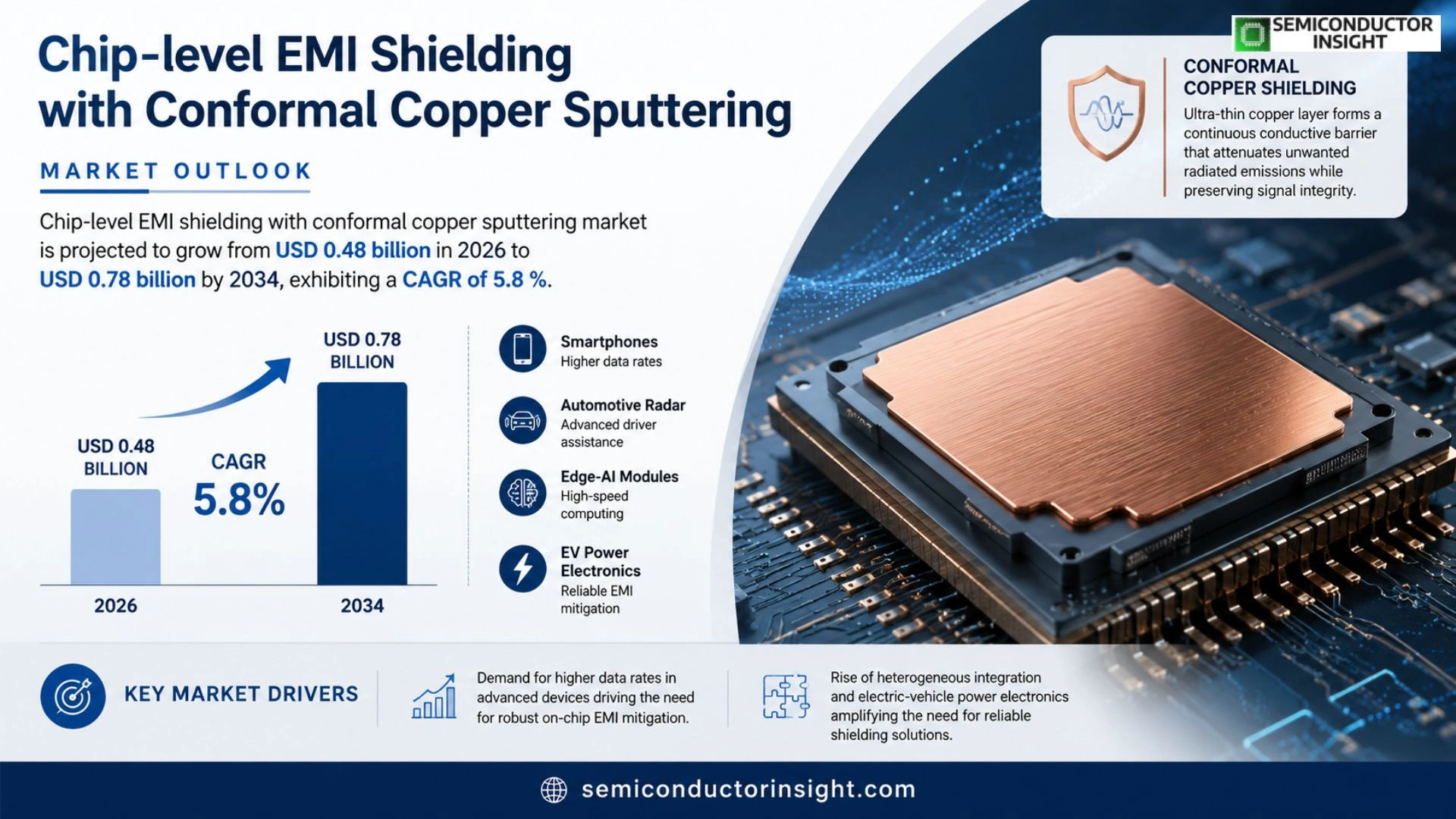
Global Chip-level EMI shielding with conformal copper sputtering market size was valued at USD 0.45 billion in 2025. The market is projected to grow from USD 0.48 billion in 2026 to USD 0.78 billion by 2034, exhibiting a CAGR of 5.8 % during the forecast period.
Chip‑level electromagnetic interference (EMI) shielding using conformal copper sputtering involves depositing ultra‑thin copper layers directly onto semiconductor packages to create a continuous conductive barrier that attenuates unwanted radiated emissions while preserving signal integrity. This technique enables higher frequency operation and supports aggressive form‑factor reduction in advanced microelectronics.
The market is accelerating because device manufacturers are pushing for higher data rates in smartphones, automotive radar, and edge‑AI modules, which demand robust on‑chip EMI mitigation. Furthermore, the rise of heterogeneous integration and the shift toward electric‑vehicle power electronics amplify the need for reliable shielding solutions.
MARKET DRIVERS
Growing Demand for Miniaturized Electronics
The rapid proliferation of IoT devices, wearables, and edge‑computing modules is forcing manufacturers to shrink form factors while maintaining performance. Chip-level EMI shielding with conformal copper sputtering Market solutions enable high‑density interconnects without compromising electromagnetic compatibility, making them indispensable for next‑generation miniaturized products.
Regulatory Push for Electromagnetic Compatibility
Stringent EMC standards in North America, Europe, and Asia‑Pacific are driving adoption of reliable shielding technologies. Companies are investing in conformal copper sputtering because it delivers uniform coverage on complex topographies, ensuring compliance with the latest regulatory thresholds.
➤ “Adoption of conformal copper sputtering has accelerated by 18% YoY as OEMs prioritize EMI performance in high‑speed chips.”
These drivers collectively bolster the confidence of investors and reinforce the long‑term growth trajectory of Chip-level EMI shielding with conformal copper sputtering Market.
MARKET CHALLENGES
High Capital Expenditure for Sputtering Equipment
State‑of‑the‑art sputtering systems require multi‑million‑dollar investments and sophisticated vacuum infrastructure. Smaller suppliers often lack the financial bandwidth to acquire such equipment, limiting market participation.
Other Challenges
Technical Integration
Integrating copper sputtering processes with existing wafer‑level fabrication lines demands precise process control. Variations in film thickness can lead to yield losses, making seamless integration a persistent hurdle.
MARKET RESTRAINTS
Limited Availability of Skilled Operators
The specialized nature of conformal copper sputtering requires operators with advanced vacuum‑technology training. A talent gap in this niche skill set restrains rapid scale‑up, especially in emerging economies.
Additionally, the steep learning curve for process optimization extends ramp‑up times, which can deter new entrants from committing resources.
Supply‑chain constraints for high‑purity copper targets also pose a restraint, as fluctuations in raw‑material availability directly impact production schedules.
MARKET OPPORTUNITIES
Emerging Applications in 5G and Automotive
The rollout of 5G infrastructure and the rise of autonomous vehicles create a surge in high‑frequency components that are highly susceptible to electromagnetic interference. Conformal copper sputtering offers a lightweight, low‑profile shielding solution perfectly suited for these applications.
Furthermore, the growing investment in advanced driver‑assistance systems (ADAS) and electric‑vehicle power electronics presents a sizable opportunity for providers that can deliver reliable, scalable shielding at chip level.
Strategic collaborations between equipment manufacturers and semiconductor fabs are expected to unlock new process windows, accelerating adoption and expanding the addressable market for Chip-level EMI shielding with conformal copper sputtering Market players.
Chip-level EMI shielding with conformal copper sputtering Market Trends
Rising Demand for High‑Frequency Chip‑Level Shielding
Chip-level EMI shielding with conformal copper sputtering Market is being propelled by the relentless push for higher data rates in smartphones, automotive radar, and edge‑AI modules. As component dimensions shrink, designers require ultra‑thin, conformal copper barriers that can be deposited directly onto semiconductor packages to suppress radiated emissions without compromising signal integrity. This technology enables operation at millimeter‑wave frequencies while supporting aggressive form‑factor reductions demanded by next‑generation devices. Manufacturers are also responding to stricter electromagnetic compatibility regulations across consumer, industrial, and automotive sectors, creating a consistent upward pressure on adoption rates worldwide.
Other Trends
Integration of Heterogeneous Systems
Heterogeneous integration of digital, analog, RF, and power blocks within a single package intensifies the need for reliable on‑chip shielding. Conformal copper sputtering delivers a continuous conductive layer that conforms to complex topographies, thereby preserving performance across mixed‑technology modules. The technique’s ability to coat high‑aspect‑ratio structures reduces the reliance on separate shielding components, streamlining assembly processes and lowering overall system cost. As manufacturers move toward system‑in‑package (SiP) architectures for 5G and autonomous‑vehicle applications, the relevance of this shielding approach continues to expand.
Equipment Expansion and Strategic Partnerships
Leading equipment providers such as Applied Materials, Lam Research, and Tokyo Electron are broadening their sputtering portfolios to address the specific needs of chip‑level EMI mitigation. A joint development announced in March 2024 between a major semiconductor fab and a copper‑coating specialist exemplifies the collaborative momentum, accelerating technology transfer across North America and Asia‑Pacific. These partnerships are not only enhancing process throughput but also improving coating uniformity and yield, thereby reinforcing supply‑chain resilience and encouraging broader market penetration.
COMPETITIVE LANDSCAPE
Key Industry Players
Chip-level EMI Shielding with Conformal Copper Sputtering: Competitive Overview
Chip‑level EMI shielding market is anchored by a handful of equipment giants that supply the high‑vacuum sputtering systems required for conformal copper deposition. Applied Materials, Lam Research, and Tokyo Electron dominate the capital‑intensive segment, leveraging extensive R&D pipelines and deep fab relationships to capture the majority of new‑equipment spend. Their platforms are increasingly integrated with advanced process control modules that address the stringent uniformity and throughput demands of 5G‑enabled smartphones, automotive radar, and edge‑AI modules. This concentration creates an oligopolistic structure where pricing power rests with the three, while smaller niche vendors pursue differentiated tooling or retrofit solutions.
Beyond the core equipment suppliers, a diverse ecosystem of material specialists and contract assemblers is shaping the market’s next growth phase. Companies such as Laird Technologies, Molex, TE Connectivity, and Amkor Technology provide proprietary copper‑based inks, plating services, and package‑level integration expertise that enable OEMs to adopt shielding without major fab re‑tooling. Semiconductor leaders including Intel, TSMC, Samsung Electronics, and Infineon Technologies are also investing in in‑house sputtering capability to secure supply chain resilience. These niche players add depth to the competitive landscape, fostering innovation in thin‑film formulations and offering end‑to‑end solutions for heterogeneous integration.
List of Key Chip-level EMI Shielding with Conformal Copper Sputtering Companies Profiled
- Applied Materials
- Lam Research
- Tokyo Electron
- Laird Technologies
- Molex
- TE Connectivity
- Amkor Technology
- Intel Corporation
- TSMC
- Samsung Electronics
- Infineon Technologies
- NXP Semiconductors
- GlobalFoundries
Segment Analysis:
| Segment Category | Sub-Segments | Key Insights |
| By Type |
|
Conformal Copper Thin‑Film
|
| By Application |
|
High‑Frequency Mobile Devices
|
| By End User |
|
Semiconductor Foundries
|
| By [Segment Category 3]] |
|
Heterogeneous Integration
|
| By [Segment Category 4]] |
|
Performance Demands
|
Regional Analysis: North America
The North American semiconductor industry is characterized by continuous innovation and investment in advanced manufacturing processes. This drives the demand for high-quality EMI shielding solutions at the chip level to protect sensitive electronic components from electromagnetic interference.
The aerospace and defense sectors in North America are significant consumers of chip-level EMI shielding. The reliability of electronic systems in these applications is paramount, making robust EMI protection a critical requirement.
The increasing integration of electronics in automobiles, including advanced driver-assistance systems (ADAS) and electric vehicle (EV) technologies, is creating new opportunities for chip-level EMI shielding.
The growing demand for high-performance computing in data centers and research institutions necessitates effective EMI shielding solutions to ensure the stability and performance of complex electronic systems.
North America
The North American market for chip-level EMI shielding with conformal copper sputtering is driven by a confluence of factors, including the region’s leadership in semiconductor innovation and the stringent regulatory environment surrounding electromagnetic compatibility. The increasing complexity of chip designs and the miniaturization trend are creating a greater need for advanced shielding solutions. Furthermore, the strong presence of aerospace and defense, automotive, and high-performance computing industries in North America contributes significantly to market growth. While the market is relatively mature, continuous innovation in conformal copper sputtering technologies and the emergence of new applications are expected to sustain growth in the coming years. The focus is shifting towards lighter, more flexible, and thermally conductive shielding materials to meet the evolving demands of modern electronic devices.
Europe
Europe presents a significant market for chip-level EMI shielding, underpinned by a robust industrial base and a strong emphasis on technological advancement. The automotive sector in Europe is a key driver of demand, with increasing electronics content and stricter EMC regulations. The aerospace and defense industries also represent substantial opportunities. European manufacturers are actively investing in research and development to enhance the performance and integration of conformal copper sputtering shielding. The market is characterized by a focus on sustainable and environmentally friendly materials, which is influencing the adoption of new shielding technologies.
Asia-Pacific
The Asia-Pacific region is poised for the highest growth in the chip-level EMI shielding market. The region’s burgeoning electronics manufacturing hubs, particularly in China, Taiwan, and South Korea, are driving significant demand. The rapid expansion of the consumer electronics industry, combined with increasing investments in automotive and industrial electronics, is fueling market growth. The increasing adoption of 5G technology and the growth of the Internet of Things (IoT) are further contributing to the demand for effective EMI shielding solutions. The region is also witnessing the emergence of local manufacturers offering competitive conformal copper sputtering shielding technologies.
South America
South America represents a smaller but growing market for chip-level EMI shielding. The increasing adoption of electronics in various industries, including telecommunications, automotive, and industrial sectors, is driving demand. The growth of the electronics manufacturing sector in Brazil and Argentina is expected to contribute to market expansion. However, the market is characterized by varying levels of economic development and regulatory complexity, which can pose challenges for market growth.
Middle East & Africa
The Middle East and Africa constitute a nascent market for chip-level EMI shielding. The increasing investments in infrastructure development, telecommunications, and industrial growth are expected to drive demand in the coming years. The growth of the automotive and aerospace industries in the region presents opportunities for market expansion. However, the market is currently limited by factors such as the relatively small electronics manufacturing base and the availability of advanced shielding technologies.
Report Scope
This market research report provides a comprehensive analysis of the Chip-level EMI shielding with conformal copper sputtering Market , covering the forecast period 2026–2034. It offers detailed insights into market dynamics, technological advancements, competitive landscape, and key trends shaping the industry.
Key focus areas of the report include:
- Market Overview: The report begins with an overview outlining its current market scenario, key growth indicators, and industry transformation drivers. It discusses macroeconomic factors, demand–supply balance, regulatory landscape, and the strategic role of semiconductors in powering advancements across industries such as automotive, telecommunications, consumer electronics, and industrial automation.
- Market Size & Forecast: Historical data and future projections for revenue, unit shipments, and market value across major regions and segments.
- Segmentation Analysis: Detailed breakdown by product type, technology, application, and end-user industry to identify high-growth segments and investment opportunities.
- Regional Insights: Insights into market performance across North America, Europe, Asia-Pacific, Latin America, and the Middle East & Africa, including country-level analysis where relevant.
- Competitive Landscape: Profiles of leading market participants, including their product offerings, R&D focus, manufacturing capacity, pricing strategies, and recent developments such as mergers, acquisitions, and partnerships.
- Technology Trends & Innovation: Assessment of emerging technologies, integration of AI/IoT, semiconductor design trends, fabrication techniques, and evolving industry standards.
- Market Drivers & Restraints: Evaluation of factors driving market growth along with challenges, supply chain constraints, regulatory issues, and market-entry barriers.
- Stakeholder Insights: Insights for component suppliers, OEMs, system integrators, investors, and policymakers regarding the evolving ecosystem and strategic opportunities.
Primary and secondary research methods are employed, including interviews with industry experts, data from verified sources, and real-time market intelligence to ensure the accuracy and reliability of the insights presented.
FREQUENTLY ASKED QUESTIONS:
What is the current market size of Chip-level EMI shielding with conformal copper sputtering Market?
-> Chip-level EMI shielding with conformal copper sputtering market size projected to grow from USD 0.48 billion in 2026 to USD 0.78 billion by 2034, exhibiting a CAGR of 5.8 %.
Which key companies operate in Chip-level EMI shielding with conformal copper sputtering Market?
-> Key players include Applied Materials, Lam Research, Tokyo Electron, among others.
What are the key growth drivers?
-> Key growth drivers include higher data rates in smartphones, automotive radar, edge‑AI modules, heterogeneous integration, and electric‑vehicle power electronics.
Which region dominates the market?
-> Asia‑Pacific is the fastest‑growing region, while North America also shows strong adoption.
What are the emerging trends?
-> Emerging trends include strategic collaborations, joint development programs, and expanded sputtering technology portfolios.
Get Sample Report PDF for Exclusive Insights
Report Sample Includes
- Table of Contents
- List of Tables & Figures
- Charts, Research Methodology, and more...


