China AI Domestic EDA Tool Chain for Advanced Process Node Design Service Market Insights
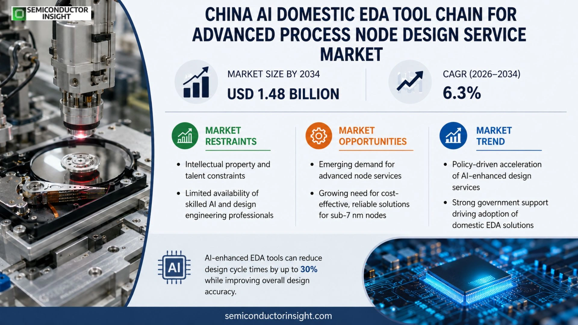
Global China AI Domestic EDA Tool Chain for Advanced Process Node Design Service Market size is projected to grow from USD 0.86 billion in 2025 to USD 1.48 billion by 2034, exhibiting a CAGR of 6.3% during the forecast period.
China AI Domestic EDA Tool Chain comprises a suite of electronic design automation (EDA) software modules,such as schematic capture, layout synthesis, timing analysis, physical verification and power optimization,augmented by artificial‑intelligence algorithms that accelerate rule extraction and pattern recognition. These services enable semiconductor designers to target advanced process nodes (7 nm and below) while reducing turnaround time and mask cost.
The market is experiencing rapid growth because Chinese semiconductor manufacturers are receiving strong policy support and multi‑year funding aimed at achieving process‑node independence. Furthermore, the rise of AI‑driven chip architectures creates demand for more intelligent verification flows. However, challenges remain due to export restrictions on certain foreign IP cores; consequently, domestic players are forming strategic alliances,such as the recent collaboration between Huawei’s HiSilicon and local EDA startups,to close capability gaps. Moreover, government incentives announced in early 2024 have accelerated adoption of AI‑enhanced design services across fabless firms.
MARKET DRIVERS
Policy Support for Domestic EDA Development
The Chinese government has introduced subsidies and tax incentives to accelerate China AI Domestic EDA Tool Chain for Advanced Process Node Design Service Market. These measures aim to reduce reliance on foreign EDA suites and foster home‑grown innovation, creating a strong growth catalyst for local vendors.
AI‑Driven Design Efficiency Gains
Advanced AI algorithms are increasingly integrated into layout optimization and timing analysis, shortening design cycles for sub‑10 nm nodes. Industry analysts observe that AI‑enabled tools can cut verification time by up to 30 %, offering a clear competitive advantage for domestic providers.
➤ “AI‑powered EDA platforms are reshaping the semiconductor design ecosystem, positioning China’s domestic players to capture a larger share of high‑value services.”
The convergence of strong policy backing, AI expertise, and a growing talent pool is solidifying the foundation for sustainable expansion of China AI Domestic EDA Tool Chain for Advanced Process Node Design Service Market.
MARKET CHALLENGES
Technology Maturity and Standardization
While AI techniques improve productivity, many domestic tools still lag behind mature international standards in terms of verification depth and interoperability. This gap can delay adoption by major fabless companies that require proven reliability.
Other Challenges
Integration Complexity
Design houses must integrate multiple AI modules,placement, routing, and power analysis,into a cohesive workflow. Managing data consistency across these modules remains a significant engineering hurdle.
MARKET RESTRAINTS
Intellectual Property and Talent Constraints
Protecting proprietary AI models and securing a skilled workforce are ongoing concerns. Limited availability of engineers with both deep learning and semiconductor design expertise restrains the speed at which domestic firms can expand their EDA suites.
MARKET OPPORTUNITIES
Emerging Demand for Advanced Node Services
As Chinese semiconductor manufacturers push toward sub‑7 nm production, demand for specialized AI‑enhanced design services is rising. Companies that can deliver reliable, cost‑effective solutions for these nodes are poised to capture new revenue streams within China AI Domestic EDA Tool Chain for Advanced Process Node Design Service Market.
China AI Domestic EDA Tool Chain for Advanced Process Node Design Service Market Trend
Policy‑Driven Acceleration of AI‑Enhanced Design Services
The Chinese semiconductor ecosystem is capitalizing on a coordinated policy agenda that couples multi‑year funding with targeted incentives for AI‑augmented design workflows. Domestic EDA providers are embedding machine‑learning modules into core functions such as schematic capture, layout synthesis, and timing analysis, thereby enabling designers to target sub‑7 nm nodes while compressing development cycles. Government directives issued in early 2024 explicitly prioritize the creation of a self‑sufficient AI‑powered tool chain, prompting fabless firms to adopt these services in order to reduce reliance on foreign IP and to meet aggressive product‑to‑market timelines. As a result, China AI Domestic EDA Tool Chain for Advanced Process Node Design Service Market is witnessing a measurable shift toward higher‑value, AI‑driven offerings that promise both speed and cost efficiency.
Other Trends
Strategic Alliances to Bridge Capability Gaps
Domestic players are responding to export restrictions by forming joint ventures and collaborative development programs. A notable example is the partnership between Huawei’s HiSilicon division and several emerging EDA startups, which pools algorithmic expertise with localized process knowledge to close functional gaps in advanced node verification. These alliances facilitate rapid knowledge transfer, co‑development of proprietary AI models, and shared access to validation datasets, thereby strengthening the overall resilience of the domestic supply chain. The collaborative environment also encourages standardization of AI‑enhanced interface protocols, which further accelerates adoption across the broader design community.
Emergence of AI‑Optimized Verification Flows
Verification has become the focal point of the next wave of AI integration, with domestic vendors delivering predictive defect detection and automated rule extraction that cut mask‑revision cycles by up to 30 %. By leveraging deep‑learning classifiers trained on historical silicon failures, these services can anticipate timing violations and power‑budget breaches before physical sign‑off, reducing costly re‑spins. The trend is supported by recent incentives that subsidize AI‑driven verification licenses for mid‑size fabless firms, fostering broader market penetration. Looking ahead, the continued refinement of AI‑optimized verification is expected to deepen the competitive edge of Chinese semiconductor designers, reinforcing the strategic importance of the AI‑enhanced EDA tool chain within the advanced process node landscape.
COMPETITIVE LANDSCAPE
Key Industry Players
China AI Domestic EDA Tool Chain for Advanced Process Node Design Services – Competitive Overview
The market is currently dominated by a few large integrated circuit (IC) groups that have built in‑house AI‑enhanced EDA capabilities to serve 7 nm and sub‑7 nm design projects. Huawei’s HiSilicon remains the de‑facto leader, leveraging its AI‑driven physical verification and power‑optimization modules to deliver end‑to‑end design services for both fabless and foundry‑backed customers. Alibaba’s Pingtouge chip division has rapidly expanded its AI‑augmented place‑and‑route suite, positioning itself as a strategic alternative for high‑performance computing and cloud‑centric workloads. Cambricon Technologies, while primarily an AI‑chip designer, contributes a proprietary timing‑analysis engine that is now offered as a commercial service to external design houses. These dominant players benefit from strong government subsidies, extensive IP portfolios, and deep collaborations with SMIC and other domestic fabs, creating a market structure that blends vertically integrated design services with specialized AI‑powered EDA modules.
Beyond the tier‑one giants, a vibrant ecosystem of niche specialists is emerging to address gaps in the AI‑enabled design flow. DeepRoute AI provides AI‑driven placement and routing that dramatically cuts iteration cycles for 5 nm designs, and its tools are increasingly licensed by regional fabless firms. Zhejiang‑based Zhuochuang EDA focuses on AI‑assisted schematic capture and rule extraction, targeting mid‑scale silicon‑photonic projects. Shenzhen EDA Technology Co., Ltd. offers a cloud‑based verification platform that integrates domestic IP libraries, while Beijing Tongyu Semiconductor delivers AI‑optimized power‑grid synthesis for automotive chips. Horizon Robotics and UNISOC have also ventured into AI‑enhanced design services, primarily supporting edge‑AI and mobile‑processor markets. Collectively, these niche players expand the domestic capability set, foster competitive pricing, and reduce reliance on foreign EDA vendors.
List of Key AI Domestic EDA Tool Chain Companies Profiled
- Huawei HiSilicon
- Alibaba Pingtouge
- Cambricon Technologies
- DeepRoute AI
- Zhuochuang EDA
- Shenzhen EDA Technology Co., Ltd.
- Beijing Tongyu Semiconductor
- Horizon Robotics
- UNISOC (Spreadtrum)
- Zhaoxin Semiconductor
- Cambricon Technologies
- Shanghai Huatai EDA
- Quantus AI EDA
- RongChuang EDA
Segment Analysis:
| Segment Category | Sub-Segments | Key Insights |
| By Type |
|
AI‑Enhanced Physical Design – Leverages deep‑learning models to predict routing congestion early, enabling designers to adjust floor‑plans before detailed placement. – Integrates pattern‑recognition engines that automatically extract reusable layout blocks from prior designs, shortening iterative cycles. – Provides adaptive optimization loops that balance performance, power, and area without manual rule tuning, fostering faster time‑to‑market for advanced nodes. |
| By Application |
|
AI Accelerator Development – Demands highly customized verification flows that can ingest neural‑network topology data directly, a capability strongly supported by AI‑augmented EDA suites. – Benefits from automated generation of data‑path pipelines, reducing manual HDL coding and allowing rapid exploration of novel compute architectures. – Encourages close collaboration between algorithm teams and layout engineers, facilitated by AI‑driven design intent translation tools. |
| By End User |
|
Fabless Chip Designers – Rely on AI‑enhanced EDA to compress design cycles, enabling them to bring differentiated products to market while staying within fab capacity constraints. – Value the ability to run iterative “what‑if” analyses without extensive manual re‑verification, a strength of modern AI‑driven tools. – Appreciate integrated cloud access that allows design teams across regions to collaborate seamlessly, aligning with government policies that promote domestic ecosystem cohesion. |
| By Integration Level |
|
Integrated Tool Suites – Offer a unified data model that eliminates hand‑offs and version mismatches between design stages, a critical advantage for advanced node projects. – Embed AI assistants that surface design recommendations contextually, reducing reliance on deep domain expertise. – Align with national initiatives encouraging end‑to‑end domestic solutions, fostering confidence among stakeholders that the entire workflow can remain within China’s ecosystem. |
| By Technology Trend |
|
AI‑Driven Design Automation – Enables rule extraction from massive legacy design libraries, allowing new projects to reuse proven patterns without manual encoding. – Supports continuous learning where the tool refines its optimization strategies based on feedback from each completed tape‑out. – Provides a strategic buffer against external technology restrictions by cultivating home‑grown intellectual property within the design flow. |
Regional Analysis: China AI Domestic EDA Tool Chain for Advanced Process Node Design Service Market
Asia-Pacific
Accelerated AI adoption in chip design, strong policy incentives, and the push for domestic supply chain resilience are primary forces driving the market’s growth across the region, especially within China’s national semiconductor roadmap.
Emerging opportunities lie in AI‑enabled verification tools, cloud‑based collaborative platforms, and specialized modules for emerging memory technologies, all tailored to the unique demands of advanced process nodes.
Domestic EDA firms are gaining ground against traditional incumbents by integrating proprietary AI algorithms, fostering fast‑track innovation cycles, and offering cost‑effective licenses to local chip designers.
Strategic government programs and export‑control policies shape the market, encouraging self‑sufficiency while guiding investment toward AI‑centric EDA capabilities for advanced node design.
North America
North America remains an influential observer of China AI Domestic EDA Tool Chain for Advanced Process Node Design Service Market, with major multinational EDA leaders closely monitoring Chinese advancements. While domestic adoption is modest, the region benefits from knowledge exchange through academic collaboration and joint research initiatives, which help refine AI‑driven design methodologies. Market participants are increasingly attentive to cross‑border partnerships that could accelerate technology transfer and foster a complementary ecosystem supportive of advanced node design worldwide.
Europe
In Europe, the focus is on benchmarking Chinese progress against its own AI‑enhanced EDA efforts. European chip designers appreciate the innovations emerging from China AI Domestic EDA Tool Chain for Advanced Process Node Design Service Market, prompting collaborative pilots and standards‑setting dialogues within industry consortia. The region’s emphasis on sustainability and design efficiency aligns with the AI‑driven optimization trends observed in Asia‑Pacific, encouraging a gradual convergence of best practices.
South America
South America’s semiconductor sector is still nascent, yet it eyes the rapid evolution of China AI Domestic EDA Tool Chain for Advanced Process Node Design Service Market as a blueprint for future growth. Regional firms are exploring training programs and technology licensing agreements that could enable them to adopt AI‑centric design flows, positioning the continent to benefit from downstream supply‑chain opportunities as global manufacturers expand their footprint.
Middle East & Africa
The Middle East & Africa region observes China AI Domestic EDA Tool Chain for Advanced Process Node Design Service Market primarily through strategic investment interest and capacity‑building initiatives. Emerging technology parks and research hubs are looking to emulate the AI‑focused design ecosystem, seeking partnerships that could introduce advanced node capabilities and foster local talent development in semiconductor engineering.
Report Scope
This market research report provides a comprehensive analysis of the China AI Domestic EDA Tool Chain for Advanced Process Node Design Service Market , covering the forecast period 2026–2034. It offers detailed insights into market dynamics, technological advancements, competitive landscape, and key trends shaping the industry.
Key focus areas of the report include:
- Market Overview: The report begins with an overview outlining its current market scenario, key growth indicators, and industry transformation drivers. It discusses macroeconomic factors, demand–supply balance, regulatory landscape, and the strategic role of semiconductors in powering advancements across industries such as automotive, telecommunications, consumer electronics, and industrial automation.
- Market Size & Forecast: Historical data and future projections for revenue, unit shipments, and market value across major regions and segments.
- Segmentation Analysis: Detailed breakdown by product type, technology, application, and end-user industry to identify high-growth segments and investment opportunities.
- Regional Insights: Insights into market performance across North America, Europe, Asia-Pacific, Latin America, and the Middle East & Africa, including country-level analysis where relevant.
- Competitive Landscape: Profiles of leading market participants, including their product offerings, R&D focus, manufacturing capacity, pricing strategies, and recent developments such as mergers, acquisitions, and partnerships.
- Technology Trends & Innovation: Assessment of emerging technologies, integration of AI/IoT, semiconductor design trends, fabrication techniques, and evolving industry standards.
- Market Drivers & Restraints: Evaluation of factors driving market growth along with challenges, supply chain constraints, regulatory issues, and market-entry barriers.
- Stakeholder Insights: Insights for component suppliers, OEMs, system integrators, investors, and policymakers regarding the evolving ecosystem and strategic opportunities.
Primary and secondary research methods are employed, including interviews with industry experts, data from verified sources, and real-time market intelligence to ensure the accuracy and reliability of the insights presented.
FREQUENTLY ASKED QUESTIONS:
What is the current market size of China AI Domestic EDA Tool Chain for Advanced Process Node Design Service Market?
-> China AI Domestic EDA Tool Chain for Advanced Process Node Design Service Market size is projected to grow from USD 0.86 billion in 2025 to USD 1.48 billion by 2034
Which key companies operate in China AI Domestic EDA Tool Chain for Advanced Process Node Design Service Market?
-> Key players include Huawei HiSilicon, SMIC, and domestic EDA startups such as eSilicon and Brite Semiconductor, which are actively expanding AI‑enhanced design capabilities.
What are the key growth drivers?
-> Key growth drivers include strong government policy support, multi‑year funding for process‑node independence, rising demand for AI‑driven chip architectures, and incentives announced in early 2024 that accelerate adoption of AI‑enhanced design services.
Which region dominates the market?
-> Asia‑Pacific, led by China, remains the dominant and fastest‑growing region due to concentrated semiconductor manufacturing and strategic national initiatives.
What are the emerging trends?
-> Emerging trends include AI‑augmented verification and rule extraction, collaborative cloud‑based design platforms, and increased integration of machine‑learning algorithms to accelerate advanced node (7 nm and below) design cycles.

Get Sample Report PDF for Exclusive Insights
Report Sample Includes
- Table of Contents
- List of Tables & Figures
- Charts, Research Methodology, and more...


