
MARKET INSIGHTS
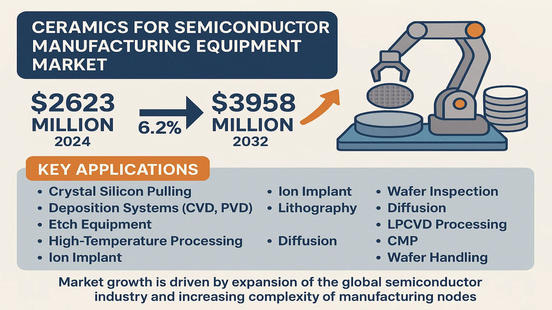
The global Ceramics For Semiconductor Manufacturing Equipment Market was valued at 2623 million in 2024 and is projected to reach US$ 3958 million by 2032, at a CAGR of 6.2% during the forecast period.
Ceramics for semiconductor manufacturing equipment are advanced, high-performance structural components engineered with exceptional material properties. These ceramics are crucial for semiconductor wafer processing and fabrication (front end) because they provide mechanical stability, thermal resistance, and corrosion resistance in highly aggressive process environments. Key applications include components for crystal silicon pulling, deposition systems (CVD, PVD, ALD), etch equipment, high-temperature processing, ion implant, lithography, wafer inspection, diffusion, LPCVD processing, CMP, and wafer handling.
The market is experiencing steady growth, primarily driven by the relentless expansion of the global semiconductor industry and the increasing complexity of manufacturing nodes. The top five players, including NGK Insulators, Kyocera, Ferrotec, Coorstek, and Niterra Co., Ltd., collectively hold a dominant market share of approximately 69%. North America is the largest regional market, accounting for about 43% of global revenue, while Semiconductor Etch Equipment represents the largest application segment with a 37% share. In terms of materials, Alumina Ceramics and Aluminum Nitride (AlN) Ceramics are the two most prominent segments, holding shares of 43% and 37% respectively, valued for their superior thermal management and electrical insulation properties.
MARKET DYNAMICS
MARKET DRIVERS
Expansion of Semiconductor Fabrication Facilities to Accelerate Market Growth
The global semiconductor industry is witnessing unprecedented expansion with over $200 billion in new fab investments announced globally between 2021-2023. This massive capital expenditure directly drives demand for advanced ceramic components essential in semiconductor manufacturing equipment. Ceramics provide critical properties including exceptional thermal stability up to 1600°C, superior corrosion resistance against aggressive process gases, and outstanding mechanical strength required in high-vacuum environments. The transition to smaller process nodes below 7nm necessitates even more sophisticated ceramic components with tighter tolerances and enhanced purity levels, further propelling market requirements. Major semiconductor manufacturers are accelerating their production capacity expansion plans to address the global chip shortage, creating sustained demand for ceramic components across etching, deposition, and wafer handling applications.
Advancements in Semiconductor Process Technologies to Fuel Ceramic Component Demand
The evolution toward 3D NAND flash memory and advanced logic chips requires increasingly complex manufacturing processes that depend heavily on specialized ceramic components. These components must maintain dimensional stability under extreme thermal cycling and resist degradation from plasma exposure during etching and deposition processes. The growing adoption of atomic layer deposition (ALD) and extreme ultraviolet (EUV) lithography technologies has created new requirements for ultra-pure ceramic materials with surface finishes below 0.1 micron roughness. Semiconductor equipment manufacturers are increasingly specifying custom ceramic solutions that can withstand the harsh conditions of modern fabrication processes while maintaining particle generation below stringent thresholds of less than 0.1 particles/cm² per processing cycle.
Increasing Complexity of Semiconductor Manufacturing Equipment to Drive Ceramic Innovation
Modern semiconductor manufacturing equipment incorporates an average of 150-200 distinct ceramic components per system, ranging from simple insulators to complex multi-material assemblies. The trend toward cluster tools that combine multiple process steps in single platforms has increased the complexity and performance requirements for ceramic components. These components must provide electrical insulation, thermal management, and structural support while maintaining vacuum integrity and minimizing contamination. The development of new ceramic materials with tailored properties, including aluminum nitride for thermal management and silicon carbide for plasma resistance, enables equipment manufacturers to achieve higher process yields and reduced downtime. Continuous innovation in ceramic manufacturing techniques, including advanced sintering processes and precision machining capabilities, supports the industry’s relentless pursuit of higher productivity and lower cost per wafer.
MARKET RESTRAINTS
High Development and Manufacturing Costs to Constrain Market Expansion
The development and production of advanced ceramic components for semiconductor equipment involve substantial investments in specialized manufacturing infrastructure and rigorous quality control processes. The requirement for ultra-high purity materials, often exceeding 99.9% purity, significantly increases raw material costs compared to conventional industrial ceramics. Manufacturing processes must maintain Class 10 or better cleanroom conditions throughout production to prevent contamination, adding considerable overhead expenses. The precision machining and finishing operations required to achieve tolerances within ±5 microns demand advanced CNC equipment and highly skilled operators, further elevating production costs. These economic factors create barriers for new market entrants and limit the adoption of ceramic components in cost-sensitive semiconductor manufacturing segments.
Technical Complexities in Ceramic Manufacturing to Hinder Market Growth
Ceramic component manufacturing for semiconductor applications faces significant technical challenges related to material consistency and reproducibility. The sintering process must achieve near-theoretical density while maintaining precise dimensional control, requiring sophisticated furnace technology with temperature uniformity within ±2°C. Differences in raw material batches can lead to variations in final component properties, necessitating extensive quality assurance protocols. The inherent brittleness of ceramic materials complicates machining operations, resulting in higher rejection rates compared to metal components. Achieving the required surface finish of better than Ra 0.2 micron often requires multiple polishing steps using diamond abrasives, increasing manufacturing time and cost. These technical hurdles limit production scalability and can cause supply chain constraints during periods of high semiconductor equipment demand.
Stringent Qualification Requirements to Delay Market Adoption
Semiconductor equipment manufacturers impose extensive qualification processes that can extend from six to eighteen months before approving new ceramic components or suppliers. These qualifications include rigorous testing for particle generation, outgassing properties, thermal cycling performance, and chemical resistance under actual process conditions. Any change in material composition or manufacturing process typically requires re-qualification, creating inertia against innovation and process improvements. The documentation requirements for traceability of raw materials and production parameters add administrative burdens and costs. These stringent qualification protocols, while necessary for ensuring process reliability, act as significant barriers to rapid technology adoption and market expansion for ceramic component suppliers.
MARKET CHALLENGES
Supply Chain Vulnerabilities and Material Sourcing Constraints to Challenge Market Stability
The ceramics for semiconductor manufacturing equipment market faces significant supply chain challenges due to the specialized nature of raw materials and limited global production capacity for high-purity ceramic powders. The majority of high-purity aluminum oxide and aluminum nitride powders originate from a concentrated supplier base, creating potential bottlenecks during periods of high demand. Geopolitical factors and trade restrictions can disrupt material availability, particularly for advanced ceramic compositions requiring rare earth additives or specialized processing aids. The energy-intensive nature of ceramic powder production and component sintering makes the industry vulnerable to energy price fluctuations and availability issues. These supply chain vulnerabilities create uncertainty in delivery schedules and pricing stability, challenging the reliable supply of ceramic components to semiconductor equipment manufacturers.
Other Challenges
Technical Workforce Shortage
The industry faces a critical shortage of technicians and engineers with expertise in advanced ceramic processing and semiconductor applications. The specialized knowledge required for developing and manufacturing semiconductor-grade ceramics typically requires 5-10 years of experience, creating a significant talent gap. Educational institutions produce limited numbers of ceramics engineering graduates, while experienced professionals are increasingly reaching retirement age. This workforce challenge hampers innovation capacity and limits the industry’s ability to respond rapidly to evolving semiconductor technology requirements.
Intellectual Property Protection
Protecting proprietary ceramic formulations and manufacturing processes presents ongoing challenges in global markets. The development of new ceramic compositions with enhanced properties requires substantial R&D investment, but reverse engineering and technology transfer risks can undermine competitive advantages. Companies must balance the need for collaboration with equipment manufacturers against the risk of intellectual property leakage, particularly in regions with less robust IP protection frameworks.
MARKET OPPORTUNITIES
Emergence of New Semiconductor Applications to Create Expansion Opportunities
The rapid development of wide bandgap semiconductor devices based on silicon carbide and gallium nitride presents substantial growth opportunities for advanced ceramic components. These devices operate at higher temperatures and power densities than traditional silicon semiconductors, requiring ceramic materials with enhanced thermal management capabilities. The manufacturing processes for wide bandgap semiconductors involve more aggressive chemistries and higher temperatures, driving demand for ceramics with superior chemical resistance and thermal stability. The market for power electronics and electric vehicle applications is projected to grow at approximately 15% annually, creating sustained demand for specialized ceramic components in the production equipment for these emerging semiconductor technologies.
Advanced Packaging Technologies to Drive Ceramic Component Innovation
The evolution toward heterogeneous integration and 3D packaging technologies creates new requirements for ceramic components in assembly and test equipment. These advanced packaging approaches involve handling and processing delicate semiconductor dies at elevated temperatures, requiring ceramics with specific thermal expansion properties matched to silicon and other semiconductor materials. The trend toward panel-level packaging and larger format processing necessitates larger ceramic components with maintained flatness and stability under thermal cycling. Equipment for advanced packaging applications increasingly incorporates ceramic elements for wafer handling, thermal management, and process chamber components, opening new market segments beyond traditional front-end semiconductor manufacturing.
Sustainability Initiatives to Foster Development of Next-Generation Ceramics
Growing emphasis on environmental sustainability in semiconductor manufacturing drives opportunities for ceramic components that enable more energy-efficient processes or reduce consumable usage. Ceramics with improved thermal insulation properties can reduce equipment energy consumption, while materials with enhanced erosion resistance extend component lifetime and reduce replacement frequency. The development of ceramic coatings and surface treatments that minimize particle generation contributes to higher process yields and reduced waste. Semiconductor manufacturers are increasingly valuing suppliers who can demonstrate environmental credentials through reduced energy consumption in manufacturing, recyclable materials, or extended product lifetimes, creating competitive advantages for ceramic component producers who prioritize sustainability in their technology development roadmaps.
CERAMICS FOR SEMICONDUCTOR MANUFACTURING EQUIPMENT MARKET TRENDS
Advanced Node Manufacturing and Miniaturization Drive Demand for High-Performance Ceramics
The relentless push towards smaller semiconductor nodes, particularly below 5nm, is fundamentally reshaping material requirements within fabrication equipment, creating a significant and sustained demand for advanced technical ceramics. These ceramics, prized for their exceptional thermal stability, corrosion resistance, and electrical insulation, are indispensable in processes like Extreme Ultraviolet (EUV) lithography and atomic layer deposition (ALD). For instance, the transition to EUV lithography, which is critical for sub-7nm chip production, requires ceramic components that can withstand intense heat and plasma environments without contaminating the ultra-clean fabrication atmosphere. This trend is directly correlated with the projected market growth from $2623 million in 2024 to $3958 million by 2032. The complexity of manufacturing these advanced components has also intensified, leading to increased R&D investment from key players who collectively hold a 69% market share, focusing on developing ceramics with even higher purity levels and superior mechanical properties to prevent particulate generation.
Other Trends
Geopolitical Reshoring and Supply Chain Security
Geopolitical tensions and a heightened focus on supply chain resilience are prompting significant investment in domestic semiconductor production capabilities across North America and Europe, which in turn fuels regional demand for specialized ceramics. Initiatives like the CHIPS and Science Act in the United States, which allocates over $52 billion in funding for domestic semiconductor research and manufacturing, are creating a direct pull for local suppliers of critical components. This is evidenced by North America’s dominant 43% share of the global market. Consequently, ceramic manufacturers are establishing or expanding production facilities within these regions to serve new and expanding fabrication plants (fabs), ensuring a secure and responsive supply chain for components essential to etch, deposition, and wafer handling equipment. This strategic localization mitigates risks associated with global logistics and aligns with national security interests concerning advanced technology.
Material Innovation for Extreme Processing Conditions
Innovation in ceramic material composition is a critical trend, driven by the need to withstand increasingly extreme processing conditions in semiconductor manufacturing. While alumina and aluminum nitride (AlN) ceramics currently dominate the market with a combined 80% share, there is growing adoption and development of silicon carbide (SiC) and silicon nitride (Si3N4) for specific high-stress applications. Silicon nitride, for example, offers a unique combination of high fracture toughness and thermal shock resistance, making it ideal for components in rapid thermal processing (RTP) equipment. Furthermore, the development of advanced composite ceramics and coatings is enhancing component longevity. These new materials are engineered to reduce particle shedding, a paramount concern in cleanroom environments, and to improve resistance to highly corrosive chemistries used in etching and cleaning chambers, thereby reducing equipment downtime and maintenance costs for fab operators.
COMPETITIVE LANDSCAPE
Key Industry Players
Companies Strive to Strengthen their Product Portfolio to Sustain Competition
The competitive landscape of the global ceramics for semiconductor manufacturing equipment market is highly consolidated, with the top five players collectively holding approximately 69% of the market share in 2024. This dominance is primarily driven by their technological expertise, extensive product portfolios, and longstanding relationships with major semiconductor equipment manufacturers. While these established players command significant market influence, numerous medium and small-sized companies operate in specialized niches, particularly within specific geographic regions or application segments.
NGK Insulators, Ltd. (Japan) stands as a preeminent leader in this market, leveraging its decades of experience in advanced ceramic engineering. The company’s dominance is particularly evident in critical applications such as semiconductor etch equipment and wafer handling systems, where its alumina and aluminum nitride components set industry standards for purity and thermal management. Following closely, Kyocera Corporation (Japan) maintains a formidable position through its vertically integrated manufacturing capabilities and continuous investment in R&D for next-generation semiconductor fabrication processes.
CoorsTek, Inc. (U.S.) and Niterra Co., Ltd. (Japan, formerly known as NGK Spark Plug Co.) also command significant market shares, each bringing distinct strengths to the forefront. CoorsTek’s strong foothold in the North American market, which accounts for approximately 43% of global demand, is complemented by its broad portfolio of advanced ceramic materials tailored for extreme semiconductor manufacturing environments. Niterra, meanwhile, capitalizes on its expertise in high-precision ceramics, particularly for deposition equipment and heat treatment applications.
Additionally, these industry leaders are actively pursuing growth through strategic initiatives. Ferrotec Holdings Corporation (Japan), another key player, is strengthening its market position through significant capacity expansions and technological partnerships, particularly in the growing Asian market. Their focus on developing ceramics for advanced packaging and heterogeneous integration aligns perfectly with industry trends toward more complex semiconductor architectures.
Meanwhile, other established materials science companies like 3M Company (U.S.) and Morgan Advanced Materials (U.K.) are leveraging their broader materials expertise to capture market share through innovative ceramic solutions for CMP equipment and ion implantation systems. These companies compete not only on technical specifications but also on their ability to provide global supply chain reliability and technical support, which has become increasingly crucial for semiconductor equipment manufacturers.
List of Key Companies Profiled
- NGK Insulators, Ltd. (Japan)
- Kyocera Corporation (Japan)
- CoorsTek, Inc. (U.S.)
- Ferrotec Holdings Corporation (Japan)
- Niterra Co., Ltd. (Japan)
- TOTO Advanced Ceramics (Japan)
- CeramTec GmbH (Germany)
- Saint-Gobain S.A. (France)
- Morgan Advanced Materials (U.K.)
- 3M Company (U.S.)
- Maruwa Co., Ltd. (Japan)
- ASUZAC Fine Ceramics (Japan)
Segment Analysis:
By Material
Alumina Ceramics Segment Commands Significant Market Share Due to Superior Mechanical Stability and Cost-Effectiveness
The market is segmented based on material into:
- Alumina Ceramics
- Subtypes: High-purity alumina, standard alumina
- AlN Ceramics
- SiC Ceramics
- Si3N4 Ceramics
- Others
- Subtypes: Zirconia, quartz, and specialized composite ceramics
By Application
Semiconductor Etch Equipment Segment Leads Due to Critical Role in Precision Patterning and High-Volume Manufacturing
The market is segmented based on application into:
- Semiconductor Deposition Equipment
- Semiconductor Etch Equipment
- Lithography Machines
- Ion Implant Equipment
- Heat Treatment Equipment
- CMP Equipment
- Wafer Handling
- Assembly Equipment
- Others
By Equipment Component
Chambers and Susceptors Segment Holds Prominence for Their Direct Exposure to Harsh Process Environments
The market is segmented based on equipment component into:
- Chambers
- Susceptors
- Heaters
- Showerheads
- Wafer Handling Components
- Subtypes: End effectors, chucks, and carriers
- Others
By Fabrication Process Node
Advanced Nodes (Below 10nm) Segment Exhibits Strong Growth Driven by Demand for Higher Performance and Miniaturization
The market is segmented based on fabrication process node into:
- Mature Nodes (Above 28nm)
- Mainstream Nodes (10nm to 28nm)
- Advanced Nodes (Below 10nm)
- Subtypes: 7nm, 5nm, 3nm, and emerging sub-3nm technologies
Regional Analysis: Ceramics For Semiconductor Manufacturing Equipment Market
North America
North America is the dominant global market for semiconductor manufacturing ceramics, holding approximately 43% of the worldwide revenue share. This leadership position is driven by the concentration of major semiconductor equipment manufacturers and advanced fabrication plants (fabs) in the United States. Significant government initiatives, such as the CHIPS and Science Act, which allocates over $52 billion in funding and incentives for domestic semiconductor research, manufacturing, and workforce development, are catalyzing massive new investments. This includes the construction of multi-billion-dollar fab facilities by companies like Intel, TSMC, and Samsung, which in turn creates substantial demand for high-performance ceramic components used in etching, deposition, and wafer handling systems. The region’s focus is on cutting-edge materials like ultra-high-purity Alumina and Aluminum Nitride (AlN) that offer exceptional thermal management, plasma resistance, and mechanical stability required for next-generation chip production at 3nm and below. Stringent quality control standards and a robust ecosystem of specialized ceramic suppliers, including CoorsTek and 3M, further solidify the region’s technological edge.
Asia-Pacific
The Asia-Pacific region represents the largest volume consumer and a critical manufacturing hub for semiconductor ceramics, fueled by the immense concentration of global semiconductor production capacity. Countries like Taiwan, South Korea, China, and Japan are home to the world’s leading foundries (TSMC, Samsung) and memory chip manufacturers, necessitating a continuous and vast supply of ceramic components. While Japan has a long-established dominance in advanced ceramic material science, with key players like NGK Insulators, Kyocera, and TOTO Advanced Ceramics, China is rapidly expanding its domestic capabilities to reduce reliance on imports, particularly for components used in mature process nodes. The region’s market is characterized by high-volume consumption, intense cost competition, and a growing emphasis on localizing the supply chain. However, the adoption of the most advanced ceramic formulations still often relies on technology from Japanese and American leaders. The ongoing geopolitical tensions and trade policies are also shaping supply chain strategies, making regional self-sufficiency a key long-term driver for ceramic material development and production within Asia.
Europe
Europe maintains a strong, technologically advanced niche within the global semiconductor ceramics market, underpinned by a robust research infrastructure and the presence of major equipment suppliers like ASML. The European Chips Act, which aims to mobilize €43 billion in public and private investments to double the EU’s global market share in semiconductors by 2030, is a significant growth driver. This initiative is fostering the development of new fabrication facilities and R&D centers, which will require advanced ceramic components. European innovation is particularly focused on specialized applications, such as ceramics for extreme ultraviolet (EUV) lithography machines, where exceptional thermal stability and vacuum compatibility are paramount. Leading European companies, such as CeramTec and Saint-Gobain, are renowned for their expertise in high-performance technical ceramics. The market is heavily influenced by strict EU regulations concerning material sourcing, sustainability, and chemical safety (REACH), which pushes innovation toward more environmentally conscious manufacturing processes for these advanced materials.
South America
The market for semiconductor manufacturing ceramics in South America is nascent and remains a minor contributor on the global stage. The region lacks significant semiconductor fabrication infrastructure, resulting in very limited local demand for these highly specialized components. Any demand is primarily met through imports from established global suppliers in North America, Europe, and Asia. Economic volatility and a historical focus on commodity exports rather than high-tech industrial development have hindered the growth of a local advanced ceramics industry capable of serving the semiconductor sector. While countries like Brazil have some electronics manufacturing, it is typically focused on assembly rather than front-end wafer processing, which limits the need for the most critical ceramic parts. The market potential is largely untapped, with growth contingent on major, long-term investments in technology and education to develop a foundational high-tech manufacturing base.
Middle East & Africa
The Middle East and Africa region represents an emerging frontier with strategic long-term potential, though its current market for semiconductor ceramics is negligible. Ambitious national visions, such as Saudi Arabia’s Vision 2030 and similar initiatives in the UAE, are promoting economic diversification into technology and advanced manufacturing. This has led to preliminary investments in building a knowledge economy and could eventually include downstream electronics packaging and assembly operations. However, the establishment of front-end semiconductor fabrication—the primary driver for ceramic component demand—is not yet a near-term reality. The region currently relies entirely on imports for any advanced ceramic needs. The key challenges include a lack of existing industrial ecosystem, specialized workforce, and R&D infrastructure. Nonetheless, sovereign wealth funds and government-backed initiatives are actively exploring partnerships and investments in the global tech sector, suggesting that the region may gradually evolve into a consumer, rather than a producer, of these advanced materials over the next decade.
Report Scope
This market research report provides a comprehensive analysis of the global and regional Ceramics for Semiconductor Manufacturing Equipment markets, covering the forecast period 2025–2032. It offers detailed insights into market dynamics, technological advancements, competitive landscape, and key trends shaping the industry.
Key focus areas of the report include:
- Market Size & Forecast: Historical data and future projections for revenue, unit shipments, and market value across major regions and segments.
- Segmentation Analysis: Detailed breakdown by material type, application, and end-user industry to identify high-growth segments and investment opportunities.
- Regional Outlook: Insights into market performance across North America, Europe, Asia-Pacific, Latin America, and the Middle East & Africa, including country-level analysis where relevant.
- Competitive Landscape: Profiles of leading market participants, including their product offerings, R&D focus, manufacturing capacity, pricing strategies, and recent developments such as mergers, acquisitions, and partnerships.
- Technology Trends & Innovation: Assessment of emerging technologies, integration of advanced materials, semiconductor fabrication techniques, and evolving industry standards.
- Market Drivers & Restraints: Evaluation of factors driving market growth along with challenges, supply chain constraints, regulatory issues, and market-entry barriers.
- Stakeholder Analysis: Insights for component suppliers, OEMs, system integrators, investors, and policymakers regarding the evolving ecosystem and strategic opportunities.
Primary and secondary research methods are employed, including interviews with industry experts

Get Sample Report PDF for Exclusive Insights
Report Sample Includes
- Table of Contents
- List of Tables & Figures
- Charts, Research Methodology, and more...







