
MARKET INSIGHTS
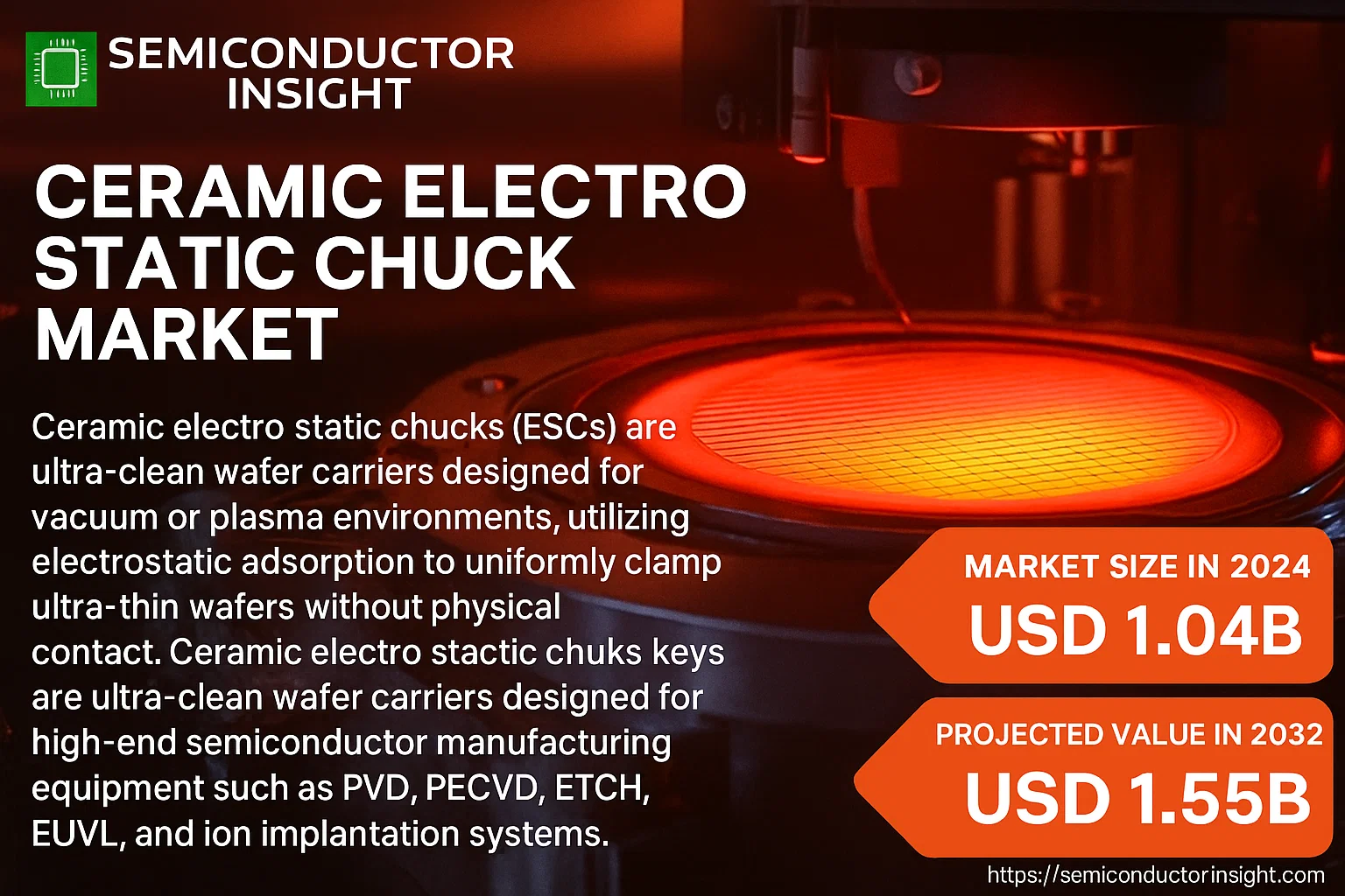
Global Ceramic Electro Static Chuck Market size was valued at USD 1.04 billion in 2024 and is projected to reach USD 1.55 billion by 2032, exhibiting a CAGR of 5.7% during the forecast period. Ceramic electro static chucks (ESCs) are ultra-clean wafer carriers designed for vacuum or plasma environments, utilizing electrostatic adsorption to uniformly clamp ultra-thin wafers without physical contact. This technology is critical in high-end semiconductor manufacturing equipment including PVD, PECVD, ETCH, EUVL, and ion implantation systems.
Ceramic ESCs function by generating an electrostatic field between a conductive base (typically metal) and an insulating layer (typically ceramic or polymer) to hold wafers with precise, uniform pressure distribution. This eliminates mechanical stress points that could damage fragile wafers, especially as wafer sizes increase to 450mm and beyond. The non-contact nature prevents particulate contamination that is critical in semiconductor fabrication where a single particle can destroy a multi-million dollar chip. The technology also enables rapid clamping and declamping (often under 1 second), significantly improving throughput compared to mechanical systems.
Market growth is driven by several key factors: the global semiconductor shortage has accelerated fab construction and equipment upgrades; the Internet of Things (IoT) and artificial intelligence (AI) are driving demand for more advanced chips requiring finer manufacturing processes; and governments are investing heavily in domestic semiconductor production for economic security. The CHIPS Act in the U.S. allocated USD 52.7 billion for semiconductor research and production, while the European Chips Act aims to mobilize EUR 43 billion in public and private investment. China’s latest five-year plan prioritizes semiconductor self-sufficiency. These initiatives directly drive demand for advanced manufacturing equipment including ESCs.
Technological advancements are also propelling the market. Leading manufacturers are developing ESCs that function at higher temperatures (up to 200°C for etch processes) and with lower leakage currents (enabling high-voltage applications like ion implantation). New materials like aluminum nitride and silicon carbide composites offer improved thermal stability and longevity. SHINKO recently introduced a model with 30% longer service life through advanced multi-layer ceramic bonding techniques.
The market faces challenges from the high cost of ceramic ESCs (typically USD 20,000-50,000 per unit) and the technical complexity of manufacturing them. However, their critical role in advanced semiconductor manufacturing ensures continued investment. The market remains concentrated with the top five manufacturers (SHINKO, NGK Insulators, NTK CERATEC, TOTO, and Sumitomo Osaka Cement) holding 79% market share collectively. Japan dominates production with 84% market share, followed by the U.S. at 10% and South Korea at 4%.
MARKET DRIVERS
Expansion in Semiconductor & Display Manufacturing
The relentless growth in demand for advanced semiconductor chips and high-resolution display panels is a primary driver for the Ceramic Electro Static Chuck (ESC) market. These components are essential fixtures within semiconductor fabrication equipment, such as etching and CVD systems, where they provide precise and stable wafer holding. The transition to smaller nodes in semiconductor manufacturing and the adoption of larger substrate sizes in the display industry necessitate ESCs with superior thermal management and surface flatness, fueling market expansion. Major investments in new fabrication plants globally, particularly for logic and memory chips, are propelling demand for high-performance ceramic ESCs.
Demand for High Thermal Stability and Process Uniformity
Ceramic ESCs are favored over their aluminum counterparts due to their excellent thermal and chemical resistance, which is critical for maintaining process stability in high-temperature vacuum environments. The push for greater yield and process uniformity in semiconductor manufacturing is driving the adoption of advanced ceramic chucks that can maintain a consistent wafer temperature with minimal deviation. This capability is paramount for processes like plasma-enhanced chemical vapor deposition (PECVD), where temperature control directly impacts film quality and device performance. The market is seeing increased demand for ESCs based on alumina (Al2O3) and aluminum nitride (AlN) ceramics due to their superior properties.
➤ The global market for ceramic ESCs is projected to grow at a compound annual growth rate (CAGR) of approximately 5.5% over the next five years, driven by sustained capital expenditure in the semiconductor sector.
Furthermore, the increasing complexity of 3D NAND and FinFET structures requires longer process times with extreme precision, making the reliable clamping and temperature control offered by ceramic ESCs indispensable. This trend is encouraging chuck manufacturers to innovate in areas like multi-zone heating and electrostatic uniformity to meet stringent process requirements.
MARKET CHALLENGES
High Cost and Complex Manufacturing
The fabrication of high-purity, high-density ceramic ESCs is a technically demanding and capital-intensive process. The need for intricate electrode patterning within the ceramic body and achieving the required surface flatness at a sub-micron level contributes to high manufacturing costs. This cost structure presents a significant barrier, particularly for smaller semiconductor equipment manufacturers or fabs operating on tight budgets. The specialized nature of the required ceramics and the need for cleanroom-compatible manufacturing further complicate the supply chain and increase the final product price.
Other Challenges
Technical Complexity in Chucking Different Wafer Types
As the industry introduces new materials like silicon carbide (SiC) and gallium nitride (GaN) for power electronics, and transitions to thinner wafers for advanced packaging, ESCs must be engineered to handle diverse electrical and thermal properties without causing damage. Developing a single ESC platform that is versatile enough for different wafer types remains a significant engineering challenge.
Contamination and Maintenance Requirements
Maintaining the dielectric surface of the chuck is critical, as any particulate contamination or film buildup can lead to arcing, poor chucking performance, and wafer defects. This necessitates regular, costly maintenance cycles and sophisticated cleaning procedures, which can lead to tool downtime and reduced overall equipment effectiveness (OEE) for fab operators.
MARKET RESTRAINTS
Capital Expenditure Cyclicality in the Semiconductor Industry
The Ceramic ESC market is intrinsically linked to the capital investment cycles of the global semiconductor industry. During periods of oversupply or economic downturn, semiconductor manufacturers sharply reduce their spending on new fabrication tools, which directly suppresses demand for ESCs. This cyclicality creates significant uncertainty for ESC suppliers, making long-term production planning and capacity investment a high-risk endeavor. The memory market, in particular, is known for its volatile investment patterns, which can lead to abrupt stops and starts in demand for critical components like ceramic chucks.
Competition from Alternative Chucking Technologies
While ceramic ESCs dominate for high-temperature processes, mechanical clamping and vacuum chucking remain viable, lower-cost alternatives for certain less-demanding applications. In processes where extreme thermal stability is not a prerequisite, equipment manufacturers may opt for these alternatives to reduce the overall system cost. This price competition restrains the market growth for ceramic ESCs in some segments of the semiconductor and flat-panel display equipment markets.
MARKET OPPORTUNITIES
Adoption in Advanced Semiconductor Packaging
The rapid growth in advanced packaging technologies, such as 2.5D and 3D IC integration, fan-out wafer-level packaging (FOWLP), and heterogeneous integration, presents a substantial growth avenue. These processes often require precise handling and thermal management of thin, delicate wafers and panels during processes like temporary bonding/debonding and through-silicon via (TSV) etching. Ceramic ESCs with optimized electrostatic forces and thermal control are well-suited to meet these challenges, opening up a new and expanding market segment beyond traditional front-end fabrication.
Growth in Compound Semiconductor and MEMS Manufacturing
The increasing production of devices based on compound semiconductors (e.g., GaN, SiC) for power electronics, RF components, and photonics, along with the steady demand for MEMS sensors, requires specialized processing equipment. These materials often involve processes that benefit from the high-temperature capability and chemical inertness of ceramic ESCs. As investments in fabs for these specialized technologies increase, the demand for application-specific ceramic ESCs is expected to rise significantly.
Development of Next-Generation ESCs for Smaller Nodes
The continued progression of semiconductor manufacturing to nodes below 3nm creates opportunities for innovation in ESC design. There is a growing need for chucks with even better uniformity, lower contamination, and the ability to handle new wafer materials and geometries. Companies that can develop ESCs with integrated sensors for real-time process monitoring, or those utilizing novel ceramic composites for enhanced performance, are poised to capture value in this high-end segment of the market.
Ceramic Electro Static Chuck Market Trends
Sustained Growth Fueled by Semiconductor Demand
The global Ceramic Electro Static Chuck market is on a steady upward trajectory, with its valuation of $1043 million in 2024 projected to reach $1551 million by 2032, representing a Compound Annual Growth Rate (CAGR) of 5.7%. This expansion is fundamentally driven by the relentless demand from the semiconductor industry, which constitutes approximately 98% of the market’s application segment. These chucks are indispensable in high-end semiconductor manufacturing processes such as PVD, PECVD, Etch, EUVL, and ion implantation, where they provide the ultra-clean, non-contact clamping essential for handling delicate wafers.
Other Trends
Dominance of Coulomb Type Technology
A key trend shaping the market is the clear preference for Coulomb Type electrostatic chucks, which command a dominant 69% share of the market by product type. This technology’s widespread adoption is attributed to its robust performance in creating the electrostatic forces necessary for secure wafer clamping in demanding vacuum and plasma environments. The basic structure, comprising a conductive base and a ceramic insulating layer with embedded electrodes, has proven exceptionally reliable for ensuring uniform clamping force and minimizing wafer distortion.
Geographical Concentration and Competitive Landscape
The market exhibits a high degree of geographical concentration, with Japan being the undisputed leader, accounting for approximately 84% of the global market. This is closely followed by the United States and South Korea, with shares of 10% and 4%, respectively. The competitive landscape is similarly consolidated, with the top five players—including SHINKO, NGK Insulators, NTK CERATEC, TOTO, and Sumitomo Osaka Cement—collectively holding a significant 79% market share. This concentration underscores the high technological barriers to entry and the critical importance of established expertise and manufacturing capabilities in this specialized field.
COMPETITIVE LANDSCAPE
Key Industry Players
Highly Concentrated Market Led by Japanese Manufacturing Giants
The global Ceramic Electro Static Chuck (ESC) market is characterized by a high degree of concentration, with the top five players accounting for approximately 79% of the market. This dominance underscores the significant technological barriers to entry and the critical importance of material science expertise and manufacturing precision. Japanese manufacturers lead the industry, a fact reflected in Japan’s commanding 84% share of the global market. Technology leaders such as SHINKO, NGK Insulators, and TOTO have established strongholds through extensive research and development, deep integration with global semiconductor equipment suppliers, and a mastery of advanced ceramic engineering required for high-performance ESCs used in processes like EUVL and ion implantation.
Beyond the market leaders, a tier of specialized and niche players contributes to the competitive dynamics. Companies like Entegris and MiCo bring strengths in materials purity and wafer handling solutions, which are crucial for contamination-sensitive semiconductor fabrication. Technetics Group offers expertise in sealing technologies that complement ESC function. Other players, including Kyocera and Krosaki Harima Corporation, leverage their broad ceramic manufacturing capabilities to serve specific application segments. While the market is mature, these companies compete on factors such as product reliability, thermal management performance, customer-specific design adaptations, and global service and support capabilities, particularly for the rapidly expanding semiconductor and flat panel display industries.
List of Key Ceramic Electro Static Chuck Companies Profiled
- SHINKO
- NGK Insulators
- NTK CERATEC
- TOTO
- Sumitomo Osaka Cement
- Entegris
- MiCo
- Kyocera
- Technetics Group
- Creative Technology Corporation
- Krosaki Harima Corporation
- AEGISCO
- Coherent
- Tsukuba Seiko
- Hebei Sinopack Electronic
Segment Analysis:
| Segment Category | Sub-Segments | Key Insights |
| By Type |
|
Coulomb Type is the dominant category due to its fundamental reliability and widespread application in standard semiconductor manufacturing processes. The principle of operation, which relies on pure electrostatic forces without direct current flow into the wafer, offers superior stability and minimal risk of contamination or damage to sensitive wafers. This makes it the preferred choice for a vast majority of high-volume production environments where process uniformity and wafer integrity are non-negotiable, cementing its position as the industry standard for advanced fabrication nodes. |
| By Application |
|
Semiconductor application is the unequivocal leader, driven by the relentless demand for smaller, more powerful chips. The critical role of electrostatic chucks in processes like etching, deposition, and ion implantation is fundamental to achieving the nanoscale precision required. The segment’s dominance reflects the extreme technical requirements of semiconductor fabs, where non-contact clamping, exceptional thermal management, and particle-free operation are essential for high yields and device performance, making it the primary driver of innovation and market growth. |
| By End User |
|
Semiconductor Fabrication Plants (Fabs) represent the most significant end-user segment. These facilities are the direct consumers of the chucks for their production lines, and their demand is propelled by global investments in new fabrication capacity and the upgrade of existing facilities to advanced nodes. The stringent requirements from these fabs for reliability, uptime, and compatibility with complex process chemistries create a highly demanding and innovation-focused customer base that dictates the performance specifications for the entire market. |
| By Material Composition |
|
Alumina (Al2O3) is the leading material due to its excellent combination of electrical insulation, mechanical strength, and plasma resistance at a relatively competitive cost. Its proven track record in harsh semiconductor environments makes it the default choice for many standard applications. While Aluminum Nitride offers superior thermal conductivity for processes requiring intense heating or cooling, the widespread adoption and manufacturing maturity of alumina-based chucks ensure their continued prevalence across a broad spectrum of etching and deposition tools. |
| By Wafer Size Compatibility |
|
300mm wafer compatibility defines the leading segment, as this is the current industry standard for high-volume manufacturing of advanced logic and memory chips. The shift to 300mm wafers over the past two decades has been driven by compelling economies of scale, and the vast majority of new capacity investments are for this size. The technical challenge of maintaining uniform electrostatic force and temperature control across the larger wafer surface has made 300mm chucks a focal point of advanced engineering, reinforcing their market leadership despite the continued operation of many legacy 200mm fabs. |
Regional Analysis: Ceramic Electro Static Chuck Market
The dominance is rooted in the region’s status as the global center for semiconductor fabrication. Leading foundries and IDMs continuously invest in new fabs, creating a perpetual and growing demand for the most advanced ceramic ESCs required for sub-7nm and 3D NAND processes, ensuring market leadership.
A mature and integrated supply chain for high-purity alumina and aluminum nitride ceramics allows for efficient and scalable ESC production. Local expertise in material science and ceramic engineering supports the development of custom solutions tailored to specific semiconductor manufacturing requirements.
Substantial national policies and financial incentives aimed at achieving semiconductor self-sufficiency are accelerating fab construction and upgrades. This direct support fosters a favorable environment for ESC manufacturers, encouraging local production and technological partnerships with equipment suppliers.
With the industry’s focus shifting to extreme ultraviolet lithography and advanced packaging, the demand for ESCs with superior thermal stability, minimal particulation, and high-precision chucking force is highest in Asia-Pacific, driving innovation and adoption of the latest product generations from suppliers.
North America
North America remains a critical and technologically advanced market for ceramic ESCs, primarily driven by leading-edge R&D activities and the presence of major semiconductor equipment OEMs. The region is characterized by a strong demand for highly specialized ESCs used in research institutions and for pilot production lines developing next-generation chip technologies. While its volume of wafer starts may be lower than Asia-Pacific, the requirements for precision, reliability, and integration with complex process tools are exceptionally high. Collaborations between equipment manufacturers, material scientists, and end-users in this region often set the global standards for ESC performance, influencing product development worldwide.
Europe
Europe holds a significant position in the ceramic ESC market, supported by a strong industrial base in power electronics, automotive semiconductors, and specialized MEMS fabrication. The region’s focus on quality and precision engineering translates into demand for high-reliability ESCs, particularly for applications requiring long lifecycles and stability in harsh processing conditions. European research initiatives often drive innovation in materials for ESCs, such as novel ceramic composites. The market is also influenced by stringent environmental and safety regulations, which push for the development of ESCs with enhanced durability and reduced consumable waste, catering to a more specialized but high-value segment.
South America
The South American market for ceramic ESCs is nascent but emerging, primarily serving local electronics assembly and a growing industrial automation sector. Demand is currently concentrated on more standardized, cost-effective ESC solutions rather than the leading-edge products seen in other regions. The market growth is linked to gradual investments in local manufacturing capabilities and technology transfer. While not a major global player, the region represents a potential growth avenue as its industrial base expands and begins to adopt more sophisticated semiconductor processing technologies over the long term.
Middle East & Africa
The ceramic ESC market in the Middle East & Africa is the smallest globally, with very limited local semiconductor fabrication presence. Demand is almost entirely tied to imports for maintenance, repair, and operations within specialty electronics and research facilities. Some countries are making strategic investments to diversify their economies into technology sectors, which could slowly foster future demand. However, currently, the market is characterized by its reliance on international suppliers and a focus on basic, reliable ESC products for non-leading-edge applications, with growth prospects being long-term and dependent on broader industrial policy shifts.
Report Scope
This market research report provides a comprehensive analysis of the Ceramic Electro Static Chuck Market , covering the forecast period 2025–2032. It offers detailed insights into market dynamics, technological advancements, competitive landscape, and key trends shaping the industry.
Key focus areas of the report include:
- Market Overview: The report begins with an overview outlining its current market scenario, key growth indicators, and industry transformation drivers. It discusses macroeconomic factors, demand–supply balance, regulatory landscape, and the strategic role of semiconductors in powering advancements across industries such as automotive, telecommunications, consumer electronics, and industrial automation.
- Market Size & Forecast: Historical data and future projections for revenue, unit shipments, and market value across major regions and segments.
- Segmentation Analysis: Detailed breakdown by product type, technology, application, and end-user industry to identify high-growth segments and investment opportunities.
- Regional Insights: Insights into market performance across North America, Europe, Asia-Pacific, Latin America, and the Middle East & Africa, including country-level analysis where relevant.
- Competitive Landscape: Profiles of leading market participants, including their product offerings, R&D focus, manufacturing capacity, pricing strategies, and recent developments such as mergers, acquisitions, and partnerships.
- Technology Trends & Innovation: Assessment of emerging technologies, integration of AI/IoT, semiconductor design trends, fabrication techniques, and evolving industry standards.
- Market Drivers & Restraints: Evaluation of factors driving market growth along with challenges, supply chain constraints, regulatory issues, and market-entry barriers.
- Stakeholder Insights: Insights for component suppliers, OEMs, system integrators, investors, and policymakers regarding the evolving ecosystem and strategic opportunities.
Primary and secondary research methods are employed, including interviews with industry experts, data from verified sources, and real-time market intelligence to ensure the accuracy and reliability of the insights presented.
FREQUENTLY ASKED QUESTIONS:
What is the current market size of Ceramic Electro Static Chuck Market?
-> Global Ceramic Electro Static Chuck Market was valued at USD 1043 million in 2024 and is projected to reach USD 1551 million by 2032, exhibiting a CAGR of 5.7% during the forecast period.
Which key companies operate in Ceramic Electro Static Chuck Market?
-> Key players include SHINKO, NGK Insulators, NTK CERATEC, TOTO, Sumitomo Osaka Cement, Entegris, MiCo, and Kyocera, among others. The top five players hold a share of about 79%.
What are the key growth drivers?
-> Key growth drivers include the critical role in high-end semiconductor manufacturing for processes like PVD, PECVD, ETCH, EUVL, and ion implantation, the advantages of uniform, non-contact clamping for delicate wafers, and the expanding global semiconductor and flat panel display industries.
Which region dominates the market?
-> Japan is the largest market for Ceramic Electro Static Chuck, holding a share of about 84%, followed by the United States and South Korea with shares of 10% and 4%, respectively.
What are the emerging trends?
-> The product’s essential function in enabling precise substrate handling and processing for high-quality semiconductor devices remains paramount. Market evolution is tied to advancements in semiconductor fabrication technologies and the increasing complexity of integrated circuits.

Get Sample Report PDF for Exclusive Insights
Report Sample Includes
- Table of Contents
- List of Tables & Figures
- Charts, Research Methodology, and more...
 Download Sample Report PDF



