MARKET INSIGHTS
The global Ceramic Coatings for Semiconductor Equipment Market size was valued at US$ 78 million in 2024 and is projected to reach US$ 109 million by 2032, at a CAGR of 4.8% during the forecast period 2025-2032.
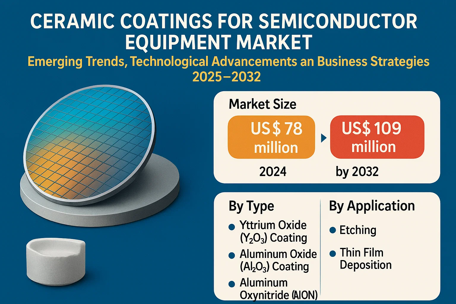
Ceramic coatings for semiconductor equipment are specialized protective layers applied to critical components like chambers, showerheads, electrostatic chucks, and liners. These coatings, primarily made of yttrium oxide (Y2O3) or aluminum oxide (Al2O3), enhance component durability in harsh semiconductor manufacturing environments. They protect against corrosive gases, plasma erosion, and particle contamination during processes like etching and thin film deposition.
The market growth is driven by increasing semiconductor production demands and stricter purity requirements in fabrication. As the global semiconductor market expands from USD 526.8 billion in 2023 to a projected USD 780.7 billion by 2030, the need for high-performance protective coatings grows accordingly. Key technologies like plasma spray coating and atomic layer deposition (ALD) methods are gaining traction for their precision and durability benefits in semiconductor applications.
MARKET DYNAMICS
MARKET DRIVERS
Rapid Growth in Semiconductor Manufacturing to Accelerate Ceramic Coatings Demand
The global semiconductor manufacturing market, valued at $251.7 billion in 2023, is projected to reach $506.5 billion by 2030, growing at a staggering CAGR of 40.49%. This extraordinary expansion directly fuels demand for ceramic coatings as semiconductor equipment components face increasingly harsh processing environments. Modern semiconductor fabrication utilizes plasma etching and chemical vapor deposition processes that generate highly corrosive fluorine and chlorine-based gases at elevated temperatures. Standard metal components degrade rapidly under these conditions, requiring advanced ceramic coatings like yttrium oxide (Y2O3) and aluminum oxide (Al2O3) that demonstrate exceptional chemical inertness and thermal stability. Industry data shows that properly coated components can achieve operational lifespans 3-5 times longer than uncoated alternatives, significantly reducing maintenance downtime in billion-dollar fabrication facilities.
Transition to Smaller Process Nodes Necessitates Advanced Coating Solutions
As semiconductor manufacturers push toward 3nm and 2nm process nodes, particulate contamination control becomes exponentially more critical. Each generational shrink in node size reduces the acceptable particulate threshold by approximately 50%, making chamber coating integrity paramount. Atomic Layer Deposition (ALD) ceramic coatings have emerged as the gold standard for these advanced nodes, achieving film uniformity with thickness variations of less than 1% across complex geometries. Leading foundries report that ALD-coated components reduce wafer defects by up to 30% compared to conventional plasma spray coatings, directly improving chip yields. This technical advantage becomes increasingly valuable as wafer production costs at leading-edge nodes exceed $15,000 per unit, where even marginal yield improvements translate to millions in additional revenue.
Government Investments in Domestic Semiconductor Production Create New Opportunities
National initiatives like the CHIPS Act in the United States and similar programs in the EU, China, and Japan are driving historic investments in domestic semiconductor manufacturing capabilities. Over $450 billion in new fabrication facilities are currently under construction globally, each requiring complete sets of coated processing equipment. These greenfield projects provide coating suppliers with opportunities to establish long-term partnerships early in the facility design phase. Recent contracts show that coating services now account for 5-8% of total equipment costs in advanced logic and memory fabs, up from just 2-3% a decade ago, reflecting the growing value of these solutions in modern semiconductor manufacturing.
MARKET RESTRAINTS
High Capital Requirements Limit Market Entry for New Players
The ceramic coating sector faces significant barriers to entry due to the specialized equipment requirements and technical expertise needed for semiconductor-grade applications. Establishing an ALD coating line capable of handling 300mm semiconductor components requires capital investments exceeding $20 million, while plasma spray systems for large chamber components demand $5-10 million setups. Furthermore, the qualification process for new coating suppliers typically takes 12-18 months, during which manufacturers must maintain expensive idle capacity. These factors concentrate market share among established players, with the top five companies currently controlling over 65% of the global ceramic coatings market for semiconductor equipment.
Technical Challenges in Coating Complex Geometries Restrict Adoption
Advanced semiconductor equipment incorporates increasingly intricate component designs such as high-aspect ratio showerheads and multi-zone electrostatic chucks that push coating technologies to their limits. Achieving uniform film thickness across these complex geometries remains technically challenging, particularly for yttria-based coatings which tend to form columnar structures that can flake under thermal cycling. Industry data indicates rejection rates for coated components can reach 15-20% for plasma spray applications and 5-8% for ALD processes, driving up total cost of ownership. These technical hurdles become particularly acute at leading-edge nodes where coating defects measuring just nanometers can impact device performance.
MARKET OPPORTUNITIES
Emerging Hybrid Coating Technologies Present Growth Potential
Innovative coating approaches combining multiple deposition methods are showing promise for next-generation semiconductor applications. Sequential plasma spray and ALD processes, for example, can deliver the bulk material properties of sprayed coatings with the precise interfacial control of ALD. Early adopters report these hybrid approaches reduce particle generation by 40-60% compared to conventional methods while achieving comparable service lifetimes. The market for such advanced coatings is projected to grow at nearly double the rate of traditional solutions as device makers seek performance improvements without complete equipment redesigns.
Expansion of Compound Semiconductor Manufacturing Creates New Demand
The rapid growth of gallium nitride (GaN) and silicon carbide (SiC) semiconductor production for power electronics and RF applications presents a significant adjacent market opportunity. These compound semiconductors require even more aggressive process conditions than silicon, with deposition temperatures exceeding 1,500°C in some cases. Specialized alumina-based ceramic coatings demonstrate particularly strong performance in these environments, with test data showing 2-3x longer service life compared to standard silicon process coatings. As the compound semiconductor market grows at a projected 30% CAGR through 2030, supporting coating services will experience parallel expansion.
MARKET CHALLENGES
Supply Chain Vulnerabilities for Coating Materials Create Risks
The ceramic coating industry faces increasing supply chain pressures for critical raw materials, particularly high-purity yttrium oxide powder. Over 85% of global yttrium production originates from China, creating single-source dependencies that became acutely visible during recent trade restrictions. Prices for 99.999% pure Y2O3 have fluctuated by up to 300% in quarterly intervals, making cost forecasting extremely challenging. Furthermore, quality variations between material batches can impact coating performance, requiring extensive requalification efforts that delay component delivery schedules by weeks or months.
Technical Workforce Shortage Constrains Production Capacity
The specialized nature of semiconductor ceramic coating operations creates significant workforce challenges, with an estimated 15,000 qualified technicians needed globally by 2025. Process engineers with expertise in both materials science and semiconductor manufacturing command premium salaries exceeding $150,000 annually in major markets, putting pressure on operating margins. Cross-training programs remain limited due to the proprietary nature of coating formulations and processes, further exacerbating the talent shortage. This skills gap becomes particularly problematic during industry upturns when coating service providers must rapidly scale operations to meet surging demand from semiconductor equipment manufacturers.
CERAMIC COATINGS FOR SEMICONDUCTOR EQUIPMENT MARKET TRENDS
Increasing Demand for High-Performance Coatings Drives Market Growth
The global semiconductor fabrication process involves extreme conditions, including corrosive plasmas, high temperatures, and reactive gases. These harsh environments necessitate durable protective coatings for critical chamber components to ensure process stability and minimize contamination. As the semiconductor market is projected to grow from $526.8 billion in 2023 to $780.7 billion by 2030, manufacturers are increasingly adopting advanced ceramic coatings like Y2O3 and Al2O3 to extend equipment lifespan. The precision requirements of sub-7nm node manufacturing have elevated coating performance standards, driving innovation in materials science and deposition techniques.
Other Trends
Transition to Atomic Layer Deposition (ALD) Technology
The semiconductor industry’s shift toward thinner, more uniform coating layers is accelerating adoption of ALD technology. Unlike conventional plasma spray coatings, ALD enables angstrom-level precision in film deposition – critical for maintaining tight critical dimension control in advanced nodes. Recent breakthroughs in thermal and plasma-enhanced ALD processes now allow for superior adhesion and density in yttrium-based coatings, with some suppliers achieving film thickness uniformity of <2% across 300mm wafers. This technical evolution is particularly crucial for etch chamber components where process drift can significantly impact yield.
Expansion of Semiconductor Capacity in Asia-Pacific
With over 60% of global semiconductor manufacturing concentrated in Asia-Pacific, regional capacity expansions are creating substantial demand for coating services. Major foundries are investing heavily in new fabs, with Taiwan, South Korea, and China accounting for 42% of global wafer capacity in 2024. This geographical concentration is driving localized coating service networks, as just-in-time maintenance requirements and stringent contamination controls favor regional suppliers. The trend is further amplified by government initiatives like China’s semiconductor self-sufficiency push, which has spurred construction of over 20 new 300mm fabs in the past three years alone.
COMPETITIVE LANDSCAPE
Key Industry Players
Innovation and Precision Driving Market Leadership in Semiconductor Ceramic Coatings
The ceramic coatings for semiconductor equipment market features a dynamic and technology-driven competitive landscape, with leading global players competing through material innovation, application expertise, and geographical reach. UCT (Ultra Clean Holdings, Inc.) has established itself as a market leader, leveraging its vertically integrated solutions and strong partnerships with major semiconductor equipment manufacturers. The company’s expertise in Y2O3 and Al2O3 coatings for chamber components has been particularly valuable as demand for advanced semiconductor manufacturing grows.
TOCALO Co., Ltd. and KoMiCo have also captured significant market share through their specialized coating technologies. TOCALO’s advanced plasma spray coating solutions are widely adopted for etch applications, while KoMiCo has strengthened its position through proprietary atomic layer deposition (ALD) techniques. Both companies continue expanding their production capacities to meet rising demand from foundries and IDMs.
The market has seen increased consolidation activities, with Enpro Industries notably expanding its capabilities through the acquisitions of LeanTeq and NxEdge. This strategic move has allowed Enpro to offer comprehensive coating solutions across the semiconductor manufacturing value chain. Similarly, Mitsubishi Chemical’s Cleanpart division has strengthened its European presence through targeted investments in coating R&D centers.
Regional specialists are also making significant impacts. Frontken Corporation Berhad dominates the Southeast Asian market with its high-performance ceramic coatings for advanced packaging applications, while WONIK QnC leads in South Korea’s memory semiconductor segment. These companies are investing heavily in next-generation coating technologies to support the transition to 3D NAND and GAA transistor architectures.
List of Key Ceramic Coating Companies Profiled
- UCT (Ultra Clean Holdings, Inc) (U.S.)
- Kurita (Pentagon Technologies) (Japan)
- Enpro Industries (LeanTeq and NxEdge) (U.S.)
- TOCALO Co., Ltd. (Japan)
- Mitsubishi Chemical (Cleanpart) (Japan)
- KoMiCo (South Korea)
- Cinos (Netherlands)
- Hansol IONES (South Korea)
- WONIK QnC (South Korea)
- Frontken Corporation Berhad (Malaysia)
- Oerlikon Balzers (Switzerland)
- Beneq (Finland)
Segment Analysis:
By Type
Y2O3 Coating Segment Leads the Market Due to Superior Corrosion Resistance in Semiconductor Equipment
The market is segmented based on material type into:
- Yttrium Oxide (Y2O3) Coating
- Aluminum Oxide (Al2O3) Coating
- Aluminum Oxynitride (AlON) Coating
- Others
By Technology
PVD & ALD Method Shows Strong Growth Potential for Precision Coatings
The market is segmented based on technology into:
- Plasma Spray Coating
- PVD & ALD Method
- Others
By Application
Etching Applications Hold Major Share Due to Increasing Semiconductor Complexity
The market is segmented based on application into:
- Etching
- Thin Film Deposition
- Others
By Component
Chamber Components Represent Largest Segment for Protection Against Harsh Conditions
The market is segmented based on component type into:
- Chambers
- Showerheads (Gas Distribution Plates)
- Electrostatic Chucks (ESC)
- Liners & Baffles
- Others
Regional Analysis: Ceramic Coatings for Semiconductor Equipment Market
North America
The North American ceramic coatings market for semiconductor equipment benefits from strong R&D investments in next-generation chip fabrication technologies, particularly in the U.S. With semiconductor giants like Intel, Texas Instruments, and Micron strategically expanding domestic production capacity (bolstered by $52 billion in CHIPS Act funding), demand for high-performance Y2O3 and Al2O3 ceramic coatings is accelerating. The region leads in adopting advanced deposition techniques such as atomic layer deposition (ALD) for wafer processing chambers and electrostatic chucks. However, supply chain constraints for rare earth materials like yttrium and strict environmental compliance requirements pose ongoing challenges for coating service providers.
Europe
Europe maintains a strong position in specialty ceramic coating technologies through advanced material science expertise, particularly in Germany and Finland. The region’s focus on sustainable semiconductor manufacturing aligns with precision coating solutions that extend component lifespan in etching and CVD applications. While market growth is steady, it faces headwinds from high operational costs and energy-intensive coating processes. Recent developments include collaborative projects between research institutions and companies like Oerlikon Balzers to develop novel nanocomposite coatings with enhanced plasma resistance for EUV lithography equipment.
Asia-Pacific
As the dominant region in semiconductor production, Asia-Pacific accounts for approximately 75% of global ceramic coating demand for semiconductor equipment. Taiwan, South Korea, and Japan collectively drive innovations in thin-film coating applications, supported by consolidated ecosystem of foundries and coating service providers. China’s aggressive semiconductor self-sufficiency push has spawned domestic ceramic coating specialists, though quality consistency remains a concern compared to established players. The region sees intense competition on coating cycle times and cost-efficiency, with plasma spray methods remaining prevalent for cost-sensitive applications despite the global shift toward PVD/ALD techniques.
South America
The South American market shows nascent growth potential, primarily serving backend semiconductor packaging operations in Brazil. Limited local coating capabilities mean most advanced semiconductor components are shipped to North America or Asia for treatment. While macroeconomic instability has hindered infrastructure investments, recent tax incentives for high-tech manufacturing in countries like Argentina could stimulate demand for basic ceramic coating services. The region currently lacks specialized coating providers for front-end semiconductor equipment.
Middle East & Africa
This emerging market is witnessing gradual growth through strategic partnerships, particularly in Israel and the UAE where governments are investing in semiconductor-related technologies. While coating service infrastructure remains underdeveloped, increasing foreign direct investment in technology parks presents long-term opportunities. Most regional demand currently involves coating refurbishment services for imported used equipment rather than new semiconductor tool coatings. The lack of domestic rare earth material processing capabilities continues to constrain market expansion.
Report Scope
This market research report provides a comprehensive analysis of the Global Ceramic Coatings for Semiconductor Equipment market, covering the forecast period 2025–2032. It offers detailed insights into market dynamics, technological advancements, competitive landscape, and key trends shaping the industry.
Key focus areas of the report include:
- Market Size & Forecast: Historical data and future projections for revenue, unit shipments, and market value across major regions and segments. The Global Ceramic Coatings for Semiconductor Equipment market was valued at USD 680 million in 2024 and is projected to reach USD 1106 million by 2032, growing at a CAGR of 7.4%.
- Segmentation Analysis: Detailed breakdown by technology (Plasma Spray Coating, PVD & ALD Method), application (Etching, Thin Film, Others), and end-user industry to identify high-growth segments and investment opportunities.
- Regional Outlook: Insights into market performance across North America, Europe, Asia-Pacific, Latin America, and Middle East & Africa, with country-level analysis for key markets like US, China, Japan, South Korea, and Germany.
- Competitive Landscape: Profiles of 30+ leading market participants including UCT, Kurita, Enpro Industries, TOCALO, and Mitsubishi Chemical, covering their product offerings, market share, R&D focus, and recent M&A activities.
- Technology Trends & Innovation: Assessment of emerging coating technologies, material innovations (Y2O3, Al2O3, AlON), and precision engineering approaches for semiconductor equipment components.
- Market Drivers & Restraints: Evaluation of factors like semiconductor industry growth (projected to reach USD 780.7 billion by 2030), wafer fabrication expansion (USD 506.5 billion by 2030), and challenges like supply chain constraints and technical specifications.
- Stakeholder Analysis: Strategic insights for semiconductor equipment manufacturers, coating service providers, material suppliers, and investors regarding market opportunities and competitive positioning.
The research employs primary interviews with industry experts and secondary data from verified sources to ensure accuracy and reliability of market insights.
FREQUENTLY ASKED QUESTIONS:
What is the current market size of Global Ceramic Coatings for Semiconductor Equipment Market?
-> Ceramic Coatings for Semiconductor Equipment Market size was valued at US$ 78 million in 2024 and is projected to reach US$ 109 million by 2032, at a CAGR of 4.8%.
Which key companies operate in this market?
-> Key players include UCT, Kurita, Enpro Industries, TOCALO, Mitsubishi Chemical, KoMiCo, Cinos, and Hansol IONES, among over 30 major competitors.
What are the key growth drivers?
-> Key growth drivers include expansion of semiconductor manufacturing (40.49% CAGR in wafer fabrication), increasing demand for advanced coating solutions, and technological advancements in semiconductor equipment.
Which region dominates the market?
-> Asia-Pacific is the dominant market, driven by semiconductor manufacturing hubs in China, Japan, South Korea, and Taiwan.
What are the emerging trends?
-> Emerging trends include development of ultra-pure coating materials, precision ALD coating techniques, and customized solutions for advanced semiconductor nodes.

Get Sample Report PDF for Exclusive Insights
Report Sample Includes
- Table of Contents
- List of Tables & Figures
- Charts, Research Methodology, and more...