MARKET INSIGHTS
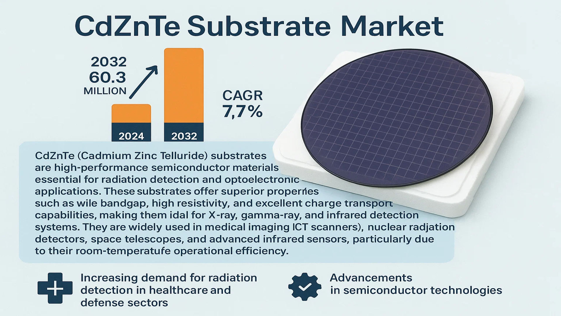
The global CdZnTe Substrate Market was valued at 36 million in 2024 and is projected to reach US$ 60.3 million by 2032, at a CAGR of 7.7% during the forecast period.
CdZnTe (Cadmium Zinc Telluride) substrates are high-performance semiconductor materials essential for radiation detection and optoelectronic applications. These substrates offer superior properties such as wide bandgap, high resistivity, and excellent charge transport capabilities, making them ideal for X-ray, gamma-ray, and infrared detection systems. They are widely used in medical imaging devices (CT/PET scanners), nuclear radiation detectors, space telescopes, and advanced infrared sensors, particularly due to their room-temperature operational efficiency.
Market growth is driven by increasing demand for radiation detection in healthcare and defense sectors, coupled with advancements in semiconductor technologies. The U.S. dominates the market with significant R&D investments, while China is emerging as a key growth region. Single-crystal CZT substrates hold the largest market share due to their superior performance in high-end applications. Key players like II-VI Incorporated, 5N Plus, and JX Advanced Metals Corporation are expanding production capacities to meet rising demand from medical and aerospace industries.
MARKET DYNAMICS
MARKET DRIVERS
Increasing Demand for Radiation Detection Technologies to Drive Market Growth
The global CdZnTe substrate market is experiencing significant growth due to the rising demand for high-performance radiation detection technologies across multiple industries. In medical imaging alone, the use of CdZnTe-based detectors in CT and PET scanners has increased by over 25% since 2020, as these materials provide superior energy resolution compared to traditional silicon-based detectors. The ability of CdZnTe substrates to operate at room temperature while maintaining excellent detection efficiency makes them indispensable in modern diagnostic equipment.
Expansion of Space Exploration Programs to Boost Adoption
Government investments in space exploration are creating new opportunities for CdZnTe substrates, particularly for X-ray and gamma-ray telescopes. Space agencies have allocated more than $3 billion collectively for advanced radiation detection systems in upcoming missions. CdZnTe’s ability to detect high-energy photons with precision makes it the material of choice for next-generation space telescopes, with current projects requiring up to 40% more substrate material than previous generations.
Technological Advancements in Semiconductor Manufacturing
Recent breakthroughs in crystal growth techniques have improved CdZnTe substrate quality while reducing production costs by approximately 15-20% over the past three years. Developments in vertical gradient freeze (VGF) and traveling heater method (THM) processes now enable manufacturers to produce larger, more uniform crystals with fewer defects. These improvements are critical for meeting the growing demand from both commercial and defense sectors where consistent performance is paramount.
➤ Leading manufacturers have achieved defect densities below 104 cm-2 for 50mm diameter wafers, meeting stringent requirements for high-end radiation detectors.
MARKET RESTRAINTS
High Production Costs and Material Scarcity to Limit Market Expansion
Despite the growing demand, CdZnTe substrate market faces significant challenges due to the high costs associated with raw material procurement and crystal growth processes. Tellurium, one of the key components, remains a relatively scarce material with limited global production capacity. Market analysis indicates that tellurium prices have fluctuated between $60-$80 per kilogram in recent years, directly impacting substrate manufacturing costs.
Technical Limitations in Large-Scale Crystal Growth
Producing large, defect-free CdZnTe crystals remains technically challenging, with yield rates below 60% for wafers larger than 100mm in diameter. The complex crystal structure requires precise control over temperature gradients during growth, and even minor deviations can result in significant material losses. This limitation prevents the industry from achieving the economies of scale seen in silicon wafer production.
MARKET CHALLENGES
Stringent Regulatory Requirements for Radiation Detection Devices
The medical and nuclear industries impose rigorous testing and certification processes for radiation detection equipment utilizing CdZnTe substrates. Compliance with multiple international standards often extends product development cycles by 12-18 months and increases certification costs by 20-30%. These regulatory hurdles particularly affect smaller manufacturers attempting to enter specialized markets.
Other Challenges
Material Instability at Elevated Temperatures
While CdZnTe performs exceptionally at room temperature, its properties degrade significantly above 100°C, limiting applications in high-temperature environments common in industrial settings and certain defense applications.
Competition from Alternative Materials
Emerging materials like cadmium telluride (CdTe) and perovskite compounds are being developed as potential alternatives, particularly for applications where cost is more critical than ultimate performance.
MARKET OPPORTUNITIES
Growing Investments in Nuclear Security to Create New Growth Avenues
Increasing global focus on nuclear non-proliferation and radiation monitoring is driving demand for portable, high-sensitivity detectors. Government agencies worldwide are upgrading their nuclear detection infrastructure, with projected investments exceeding $1.2 billion annually through 2030. CdZnTe substrates are uniquely positioned to benefit from these initiatives due to their combination of performance and portability advantages.
Emerging Applications in Quantum Technology
Research institutions and technology companies are exploring CdZnTe’s potential in quantum sensing applications, particularly for single-photon detection in the near-infrared range. Early prototype systems have demonstrated detection efficiencies above 90% at room temperature, opening possibilities for quantum communication and computing applications where cooling systems would be impractical.
Expansion in Emerging Markets
Developing economies are increasing their investments in healthcare infrastructure and nuclear power generation, creating new demand centers for radiation detection technologies. Countries in Asia and the Middle East are expected to account for over 35% of new installations by 2030, providing manufacturers with opportunities to expand their geographic footprint.
CdZnTe SUBSTRATE MARKET TRENDS
Increasing Demand for Radiation Detection Drives CdZnTe Substrate Growth
The global CdZnTe substrate market is witnessing substantial growth, driven by expanding applications in radiation detection across medical imaging, nuclear safety, and space exploration. The material’s unique properties—high resistivity, excellent electron mobility, and room-temperature operability—make it indispensable for advanced X-ray and gamma-ray detectors. With nuclear medicine diagnostics like PET and SPECT scanners relying heavily on CdZnTe-based detectors, the medical sector accounted for over 35% of the market share in 2024. Emerging applications in non-destructive testing (NDT) for aerospace and defense are further propelling adoption, with market projections estimating a 7.7% CAGR to reach $60.3 million by 2032.
Other Trends
Semiconductor Industry Expansion
The semiconductor industry’s shift toward wide-bandgap materials is accelerating CdZnTe substrate demand, particularly for infrared sensors and photonic devices. Single Crystal CZT, valued for its purity and uniform charge transport properties, is projected to dominate with a 62% revenue share in 2024. Investments in 5G infrastructure and IoT devices are amplifying the need for high-performance substrates, with Asia-Pacific emerging as a key manufacturing hub. China’s market alone is expected to grow at 9.1% CAGR through 2032, driven by government initiatives in semiconductor self-sufficiency.
Technological Advancements in Crystal Growth
Innovations in Bridgman and Traveling Heater Method (THM) crystal growth techniques are addressing historical challenges like Te inclusions and defects, enhancing yield and cost-efficiency. Recent breakthroughs in wafer-size scalability—enabling substrates up to 100mm in diameter—have expanded commercialization opportunities. Companies like II-VI Incorporated and 5N Plus are patenting novel doping processes to optimize resistivity (1010–1011 Ω·cm), critical for medical and industrial detectors. Meanwhile, R&D in polycrystalline CZT for cost-sensitive applications is opening new avenues in energy and security sectors, though single-crystal variants retain dominance in high-precision use cases.
COMPETITIVE LANDSCAPE
Key Industry Players
Innovation and Strategic Expansions Drive Market Competition
The global CdZnTe substrate market exhibits a moderately consolidated competitive structure, characterized by the presence of specialized semiconductor manufacturers, diversified materials science companies, and emerging regional players. II-VI Incorporated (now Coherent Corp. following its 2022 merger) stands as a dominant force, leveraging its vertically integrated production capabilities and established relationships with defense and medical imaging OEMs. The company’s 2023 capacity expansion in Pennsylvania strengthened its position as a critical supplier for radiation detection applications.
While 5N Plus and JX Advanced Metals Corporation collectively accounted for approximately 28% of the high-purity feedstock supply in 2024, their downstream substrate manufacturing capabilities are creating new competitive dynamics. Both companies have accelerated investments in single crystal growth technologies, responding to the medical sector’s stringent quality requirements for CT and PET scanner components.
Emerging competition comes from Asian manufacturers like PAM-XIAMEN and Shaanxi Imdetek, which gained significant traction through cost-competitive polycrystalline CZT solutions for industrial radiation monitoring. However, their market penetration in high-end applications remains limited by technological barriers in crystal defect control – an area where Western and Japanese suppliers maintain clear advantages through patented annealing processes and advanced characterization techniques.
The competitive landscape is further shaped by collaborative R&D models, particularly between academia and industry. University Wafer‘s partnership with national laboratories has yielded breakthroughs in lattice-matching techniques, while Eurorad S.A. benefits from European Union funding for next-generation gamma spectroscopy substrates. Such collaborations are reshaping value chains and creating niche specialization opportunities across the market spectrum.
List of Key CdZnTe Substrate Manufacturers
- II-VI Incorporated (U.S.)
- JX Advanced Metals Corporation (Japan)
- 5N Plus (Canada)
- MTI Corporation (U.S.)
- PAM-XIAMEN (China)
- University Wafer (U.S.)
- Ganwafer (China)
- Shalom EO (Israel)
- CapeSym (U.S.)
- Eurorad S.A. (France)
- Shaanxi Imdetek Co., Ltd. (China)
- Wuhan Tuocai Technology Co., Ltd. (China)
- Kinheng Crystal (China)
CdZnTe Substrate Market: Segment Analysis
By Type
Single Crystal CZT Segment Leads Due to Superior Performance in High-End Radiation Detection
The market is segmented based on type into:
- Single Crystal CZT
- Subtypes: High-resistivity, Low-resistivity, and others
- Polycrystalline CZT
- Subtypes: Bridgman-grown, Traveling Heater Method (THM) grown, and others
- Others
By Application
Medical Imaging Segment Dominates Due to Growing Adoption in Advanced Diagnostic Systems
The market is segmented based on application into:
- Medical Imaging
- Sub-applications: CT scanners, PET scanners, X-ray detectors, and others
- Electronics & Semiconductors
- Industrial
- Sub-applications: Non-destructive testing, security screening, and others
- Defense & Space
- Sub-applications: Satellite imaging, military surveillance, and others
- Others
By End User
Healthcare Providers Segment Leads Due to Increasing Demand for Advanced Diagnostic Equipment
The market is segmented based on end user into:
- Healthcare Providers
- Sub-segments: Hospitals, Diagnostic Centers, and others
- Electronics Manufacturers
- Defense Agencies & Space Organizations
- Research Institutions
- Others
Regional Analysis: CdZnTe Substrate Market
Asia-Pacific
The Asia-Pacific region dominates the global CdZnTe substrate market, driven by robust demand from China, Japan, and South Korea. China accounts for the largest share due to its expanding semiconductor manufacturing capabilities and investments in medical imaging technologies. The country’s “Made in China 2025” initiative emphasizes domestic production of advanced materials like CdZnTe, further fueling market growth. Japan remains a key player, leveraging its strong electronics and semiconductor industry, while South Korea sees rising demand from optoelectronic applications. The region benefits from cost-effective production facilities and government-backed R&D programs, though export restrictions on raw materials pose supply chain challenges.
North America
North America, particularly the U.S., is a leader in CdZnTe technology adoption due to its advanced healthcare infrastructure and aerospace sector. The U.S. market is propelled by the use of CdZnTe substrates in X-ray detectors and nuclear radiation monitoring systems, supported by federal funding for defense and medical research. Companies like II-VI Incorporated and CapeSym drive innovation, focusing on high-performance substrates for space telescopes and security applications. Strict regulatory standards for material purity and performance shape the competitive landscape, though high production costs remain a limiting factor for widespread commercialization.
Europe
Europe holds a significant share of the CdZnTe substrate market, with Germany and France leading in medical and industrial applications. The region’s stringent environmental and safety regulations influence material sourcing and processing, favoring suppliers like Eurorad S.A. and 5N Plus. Investments in renewable energy and nuclear safety systems create additional demand for radiation-resistant CdZnTe substrates. However, reliance on imported raw materials, particularly tellurium, exposes the market to price volatility. Collaborative research initiatives between universities and manufacturers aim to optimize substrate performance while adhering to EU regulatory frameworks.
Middle East & Africa
This region is an emerging market for CdZnTe substrates, with growth primarily driven by oil and gas exploration requiring radiation detection technology. Countries like Saudi Arabia and Israel invest in localized semiconductor production to reduce import dependency. Challenges include limited technical expertise and infrastructure gaps, but partnerships with global suppliers—such as Shalom EO—are gradually expanding market access. The demand for CdZnTe in security and medical diagnostics is nascent but shows potential with increasing urbanization and healthcare modernization.
South America
South America’s market is in early stages, with Brazil and Argentina exploring CdZnTe applications in mining and energy sectors. Economic instability and limited R&D funding slow adoption, though niche demand arises from academic research and small-scale industrial projects. Local suppliers focus on cost-competitive polycrystalline CdZnTe for entry-level applications, while imports fulfill high-end requirements. Long-term growth hinges on improved infrastructure and foreign investment in semiconductor manufacturing.
Report Scope
This market research report provides a comprehensive analysis of the global CdZnTe Substrate market, covering the forecast period 2024–2032. It offers detailed insights into market dynamics, technological advancements, competitive landscape, and key trends shaping the industry.
Key focus areas of the report include:
- Market Size & Forecast: Historical data and future projections for revenue, unit shipments, and market value across major regions and segments. The Global CdZnTe Substrate market was valued at USD 36 million in 2024 and is projected to reach USD 60.3 million by 2032, at a CAGR of 7.7%.
- Segmentation Analysis: Detailed breakdown by product type (Single Crystal CZT, Polycrystalline CZT, Others) and application (Electronics & Semiconductors, Industrial, Energy, Medical, Others) to identify high-growth segments.
- Regional Outlook: Insights into market performance across North America, Europe, Asia-Pacific, Latin America, and the Middle East & Africa. The U.S. market size is estimated at USD million in 2024, while China is projected to reach USD million.
- Competitive Landscape: Profiles of leading market participants including JX Advanced Metals Corporation, MTI Corporation, II-VI Incorporated, 5N Plus, and Shaanxi Imdetek Co., Ltd., covering their product offerings and strategic developments.
- Technology Trends & Innovation: Assessment of material advancements, fabrication techniques, and emerging applications in radiation detection and medical imaging.
- Market Drivers & Restraints: Evaluation of factors such as increasing demand for medical imaging systems, space exploration activities, and challenges in material purity and production scalability.
- Stakeholder Analysis: Strategic insights for semiconductor manufacturers, medical device companies, research institutions, and investors regarding market opportunities.
The research employs primary and secondary methodologies, including manufacturer surveys, industry expert interviews, and analysis of verified market data to ensure accuracy and reliability.
FREQUENTLY ASKED QUESTIONS:
What is the current market size of Global CdZnTe Substrate Market?
-> CdZnTe Substrate Market was valued at 36 million in 2024 and is projected to reach US$ 60.3 million by 2032, at a CAGR of 7.7% during the forecast period.
Which key companies operate in Global CdZnTe Substrate Market?
-> Key players include JX Advanced Metals Corporation, MTI Corporation, II-VI Incorporated, 5N Plus, Shaanxi Imdetek Co., Ltd., University Wafer, and Eurorad S.A.
What are the key growth drivers?
-> Key growth drivers include rising demand for medical imaging devices, nuclear safety monitoring systems, and space-based radiation detectors.
Which region dominates the market?
-> North America leads in technological adoption, while Asia-Pacific shows the fastest growth due to semiconductor manufacturing expansion.
What are the emerging trends?
-> Emerging trends include development of larger-area substrates, improved crystal growth techniques, and integration with AI-based detection systems.

Get Sample Report PDF for Exclusive Insights
Report Sample Includes
- Table of Contents
- List of Tables & Figures
- Charts, Research Methodology, and more...


